EP2713280A2 - Handgeführte vorrichtung, usb-ladegerät und verfahren zur identifizierung des usb-ladegerätes durch die handgeführte vorrichtung - Google Patents
Handgeführte vorrichtung, usb-ladegerät und verfahren zur identifizierung des usb-ladegerätes durch die handgeführte vorrichtung Download PDFInfo
- Publication number
- EP2713280A2 EP2713280A2 EP11795209.3A EP11795209A EP2713280A2 EP 2713280 A2 EP2713280 A2 EP 2713280A2 EP 11795209 A EP11795209 A EP 11795209A EP 2713280 A2 EP2713280 A2 EP 2713280A2
- Authority
- EP
- European Patent Office
- Prior art keywords
- hand held
- held device
- usb charger
- identification information
- charging
- Prior art date
- Legal status (The legal status is an assumption and is not a legal conclusion. Google has not performed a legal analysis and makes no representation as to the accuracy of the status listed.)
- Granted
Links
Images





Classifications
-
- H—ELECTRICITY
- H02—GENERATION; CONVERSION OR DISTRIBUTION OF ELECTRIC POWER
- H02J—ELECTRIC POWER NETWORKS; CIRCUIT ARRANGEMENTS OR SYSTEMS FOR SUPPLYING OR DISTRIBUTING ELECTRIC POWER; SYSTEMS FOR STORING ELECTRIC ENERGY
- H02J7/00—Circuit arrangements for charging or discharging batteries or for supplying loads from batteries
- H02J7/40—Circuit arrangements for charging or discharging batteries or for supplying loads from batteries characterised by the exchange of charge or discharge related data
- H02J7/44—Circuit arrangements for charging or discharging batteries or for supplying loads from batteries characterised by the exchange of charge or discharge related data between battery management systems and power sources
-
- G—PHYSICS
- G06—COMPUTING OR CALCULATING; COUNTING
- G06F—ELECTRIC DIGITAL DATA PROCESSING
- G06F1/00—Details not covered by groups G06F3/00 - G06F13/00 and G06F21/00
- G06F1/26—Power supply means, e.g. regulation thereof
-
- G—PHYSICS
- G06—COMPUTING OR CALCULATING; COUNTING
- G06F—ELECTRIC DIGITAL DATA PROCESSING
- G06F11/00—Error detection; Error correction; Monitoring
- G06F11/006—Identification
-
- G—PHYSICS
- G06—COMPUTING OR CALCULATING; COUNTING
- G06F—ELECTRIC DIGITAL DATA PROCESSING
- G06F13/00—Interconnection of, or transfer of information or other signals between, memories, input/output devices or central processing units
- G06F13/38—Information transfer, e.g. on bus
- G06F13/40—Bus structure
- G06F13/4063—Device-to-bus coupling
- G06F13/4068—Electrical coupling
-
- G—PHYSICS
- G06—COMPUTING OR CALCULATING; COUNTING
- G06F—ELECTRIC DIGITAL DATA PROCESSING
- G06F2213/00—Indexing scheme relating to interconnection of, or transfer of information or other signals between, memories, input/output devices or central processing units
- G06F2213/0042—Universal serial bus [USB]
-
- H—ELECTRICITY
- H02—GENERATION; CONVERSION OR DISTRIBUTION OF ELECTRIC POWER
- H02J—ELECTRIC POWER NETWORKS; CIRCUIT ARRANGEMENTS OR SYSTEMS FOR SUPPLYING OR DISTRIBUTING ELECTRIC POWER; SYSTEMS FOR STORING ELECTRIC ENERGY
- H02J7/00—Circuit arrangements for charging or discharging batteries or for supplying loads from batteries
-
- H—ELECTRICITY
- H02—GENERATION; CONVERSION OR DISTRIBUTION OF ELECTRIC POWER
- H02J—ELECTRIC POWER NETWORKS; CIRCUIT ARRANGEMENTS OR SYSTEMS FOR SUPPLYING OR DISTRIBUTING ELECTRIC POWER; SYSTEMS FOR STORING ELECTRIC ENERGY
- H02J7/00—Circuit arrangements for charging or discharging batteries or for supplying loads from batteries
- H02J7/40—Circuit arrangements for charging or discharging batteries or for supplying loads from batteries characterised by the exchange of charge or discharge related data
- H02J7/47—Arrangements for checking compatibility or authentication between one component, e.g. a battery or a battery charger, and another component, e.g. a power source
-
- Y—GENERAL TAGGING OF NEW TECHNOLOGICAL DEVELOPMENTS; GENERAL TAGGING OF CROSS-SECTIONAL TECHNOLOGIES SPANNING OVER SEVERAL SECTIONS OF THE IPC; TECHNICAL SUBJECTS COVERED BY FORMER USPC CROSS-REFERENCE ART COLLECTIONS [XRACs] AND DIGESTS
- Y02—TECHNOLOGIES OR APPLICATIONS FOR MITIGATION OR ADAPTATION AGAINST CLIMATE CHANGE
- Y02E—REDUCTION OF GREENHOUSE GAS [GHG] EMISSIONS, RELATED TO ENERGY GENERATION, TRANSMISSION OR DISTRIBUTION
- Y02E60/00—Enabling technologies; Technologies with a potential or indirect contribution to GHG emissions mitigation
- Y02E60/10—Energy storage using batteries
Definitions
- the present application relates to the field of hand held device charger technologies, and in particular, to a hand held device, a USB charger, and a method for a hand held device to identify a USB charger.
- a USB charger includes a charging head and a power cable, where the charging head possesses a type A USB interface, and the power cable is a USB transmission line, and the type A USB interface includes four pins including VBUS, D+, D-, and GND, where the VBUS pin is configured as the positive pole of an output direct current power supply, and the GND is configured as the negative pole of the output direct current power supply, and the USB transmission line and the charging head of the USB charger involved in the present application are an integrated and fixed connection structure.
- a standard USB charger short-circuits the D+ pin and the D- pin inside the charging head at its charging head side and they are not connected to any other part of the charging head.
- the hand held device side identifies, by determining whether the D+ pin and the D- pin are short-circuited, a standard USB charger.
- USB charger that matches the hand held device to charge the hand held device
- the so-called USB charger that matches the hand held device is in compliance with the standard USB charger rule and the hand held device may only be charged by a USB charger that matches the hand held device.
- short-circuiting the D+ pin and the D-pin at the charging head side of a USB charger is a connection character possessed by all the standard USB chargers
- the hand held device may not identify, only by determining whether the D+ pin and the D- pin are short-circuited, the USB charger that matches the hand held device, thereby failing to ensure the charging safety of the hand held device.
- embodiments of the present application provide a hand held device, a USB charger, and a method for the hand held device to identify the USB charger, so that the hand held device can exclusively identify its matching charger to ensure charging safety of the hand held device.
- a hand held device where a charging interface thereof is a universal serial bus USB interface, including 5 pins: VBUS, D+, D-, ID, and GND, where the VBUS pin is a positive pole of an input power supply and the GND is a negative pole of the input power supply, further including: an identification information acquisition module and a charging control circuit, where the identification information acquisition module, connected between the charging control circuit and a non-power pin of the hand held device charging interface, is configured to acquire the identification information of a USB charger, and the non-power pin is the D+ pin, the D- pin, or the ID pin; and the charging control circuit is configured to receive the identification information of the USB charger provided by the identification information acquisition module and use the identification information to identify a USB charger that matches the hand held device.
- a charging interface thereof is a universal serial bus USB interface, including 5 pins: VBUS, D+, D-, ID, and GND, where the VBUS pin is a positive pole of an input power supply and the GND is a negative pole of
- a universal serial bus interface charger including a universal serial bus interface at one end connected to a hand held device, the universal serial bus interface including 5 pins: VBUS, D+, D-, ID, and GND, where the VBUS pin is a positive pole of an output power supply and the GND pin is a negative pole of the output power supply, and a non-power pin is connected to an identification information module, configured to provide identification information of USB charger identity information, and the non-power pin is the ID pin, the D+ pin, or the D- pin.
- a method for a hand held device to identify a matching universal serial bus interface charger including:
- a USB charger charging interface involved in embodiments of the present invention connected to a hand held device and a hand held device charging interface are both type B USB interfaces or Micro USB interfaces, including 5 pins: VBUS, D-, D+, ID, and GND, where the VBUS pin is a positive pole of an output power supply, the GND is a negative pole of the output power supply, and the other 3 pins are not used, and these 3 unused pins are non-power pins.
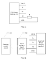
- FIG. 1 shows a schematic structural diagram of a USB charger charging interface of an embodiment of the present application.
- An identification information module 100 is added to the USB charger charging interface, and is configured to provide the USB charger with identification information that is capable of identifying the identity of the USB charger.
- the USB charger charging interface is a type B USB interface or a Micro USB interface, including 5 pins: VBUS, D-, D+, ID, and GND, where the VBUS pin is a positive pole of a power supply, and the GND pin is a negative pole of the power supply, and the 3 pins D-, D+, and ID are called non-power pins, and the identification information module 100 is connected to the ID pin.
- FIG. 1 is only a specific schematic diagram of the USB charger charging interface, and the identification information module 100 may also be connected to the D- pin or the D+ pin, which is not limited by the present application.
- FIG. 2 shows a schematic structural diagram of a hand held device charging interface that matches the USB charger joint shown in FIG. 1 , and an identification information acquisition module 200 is added between the hand held device charging interface and a charging control electricity 300 to acquire the identification information of the USB charger.
- the hand held device charging interface is a type B USB interface or a Micro USB interface, including 5 pins: VBUS, D-, D+, ID, and GND, where the VBUS pin is the positive pole of a power supply, and the GND pin is the negative pole of the power supply, and the 3 pins D-, D+, and ID are called non-power pins, an input end of the identification information acquisition module 200 is connected to the ID pin, and an output end of the identification information acquisition module 200 is connected to the charging control circuit 300.
- the identification information acquisition module 200 When the USB charger charging joint is inserted into the hand held device charging interface, the identification information acquisition module 200 is electrically connected to the identification information module 100, and the identification information acquisition module 200 acquires the identification information inside the identification information module 100 and identifying the USB charger, and provides it to the charging control circuit 300, and the charging control circuit 300 determines whether the identification information is standard identification information, and if yes, the hand held device identifies the USB charger and uses the USB charger for charging; otherwise, the hand held device cannot identify the USB charger and cannot use the USB charger for charging accordingly, thereby ensuring the charging safety of the hand held device.
- FIG. 2 is only a specific schematic diagram of the hand held device charging interface
- the identification signal acquisition module may also be connected to the D- pin or the D+ pin
- the non-power pin connected to the identification information acquisition module corresponds to the pin connected to the label information module 100, which is not limited by the present application.
- the identification information module in the embodiment corresponding to FIG. 1 may be a detecting resistance R, or an identification information memory that stores identity identification information of the USB charger.
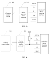
- FIG. 3a shows a circuit conceptual diagram of a USB charger charging joint.
- the charging joint is a type B USB interface or a Micro USB interface, including 5 pins: VBUS, D-, D+, ID, and GND, where the VBUS pin is a positive pole of an output power supply, and the GND is a negative pole of the output power supply, and the identification information module 100 is a detecting resistance R, and the detecting resistance R is connected between the ID pin and the GND pin.
- the hand held device By detecting the voltage signal on the detecting resistance R, the hand held device identifies whether the USB charger is a matching USB charger of the hand held device.
- the identification information module inside the USB charger is a detecting resistance
- two implementation manners are available for the identification information acquisition module inside the hand held device.
- One is implementation through an active analog to digital converter, and the other is implementation through a passive analog to digital converter and a direct current power supply.
- the identification information acquisition module is an active analog to digital converter.
- FIG. 3b shows a schematic structural diagram of a hand held device charging interface that matches the USB charger charging joint shown in FIG. 3a .
- the charging interface is a type B USB interface or a Micro USB interface, including 5 pins: VBUS, D-, D+, ID, and GND, where the VBUS pin is the positive pole of an output power supply and the GND is the negative pole of the output power supply, and different from the embodiment corresponding to FIG. 2 , the identification information acquisition module specifically is an active analog to digital converter 210.
- an input end of the active analog to digital converter 210 is connected to the ID pin of the hand held device charging interface, and an output end of the active analog to digital converter 210 is connected to a charging control circuit 300 inside the hand held device, and the active analog to digital converter 210 is capable of providing a power supply for a detecting resistance and is capable of acquiring the voltage drop on the detecting resistance R.
- the power supply inside the active analog to digital converter 210 forms a closed loop with the detecting resistance R inside the USB charger, and there is current flowing in the closed loop, and voltage drop is generated on the detecting resistance R, and the active analog to digital converter 210 acquires the voltage drop on the detecting resistance R, converts it to a digital signal and provides it to the charging control circuit 300.
- the output current of the active analog to digital converter 210 is fixed, and the resistance value of the detecting resistance R is fixed.
- the charging control circuit 300 compares the acquired voltage drop on the detecting resistance R with a standard voltage range, and when the voltage drop on the detecting resistance R is within the standard voltage range, an identification signal is output to connect the charging loop of the hand held device and the USB charger, and the hand held device is capable of using the USB charger for charging; otherwise, the charging control loop 300 outputs that the signal cannot be identified, and the charging loop of the hand held device and the USB charger cannot form a closed loop, that is, the hand held device cannot use the USB charger for charging, thereby ensuring the charging safety of the hand held device.
- the resistance values of detecting resistances connected in series in USB chargers of the same model may be the same, and the output current of active analog to digital converters 210 inside the hand held devices of the same model may be set to a same value.
- the hand held devices of the same model may identify and use the corresponding USB chargers of the same model, so that a certain hand held device may use one type of USB chargers corresponding to the hand held device model for charging.
- the following uses a specific application example to describe the identification process of a hand held device and a USB charger:
- the output current I of the active analog to digital converter 210 flows through the detecting resistance R and generates a voltage drop on the detecting resistance R. Then, the active analog to digital converter 210 acquires the voltage drop U R on the detecting resistance R, converts the voltage signal U R to a digital signal and provides it to the charging control circuit 300.
- the charging control circuit 300 detects that the voltage UR of the detecting resistance R is within a range of [0.475V, 0.525V], the identification signal is output to connect the charging loop of the hand held device and the USB charger so that the hand held device uses the USB charger for charging; otherwise, the charging control loop 300 outputs that the signal cannot be identified, and the charging loop of the hand held device and the USB charger cannot form a closed loop, that is, the hand held device cannot use the USB charger for charging, thereby ensuring the charging safety of the hand held device.
- the identification information acquisition module is a passive analog to digital converter and a direct current power supply.
- FIG. 3c shows a schematic structural diagram of another hand held device charging interface that matches the USB charger charging joint shown in FIG. 3a .
- the identification information acquisition module specifically is implemented by a passive analog to digital converter 220 and a direct current power supply VDD.
- an input end of the passive analog to digital converter 220 is connected to the ID pin of the hand held device charging interface, and an output end of the passive analog to digital converter 220 is connected to the charging control circuit 300 inside the hand held device, and the direct current power supply VDD is connected to the ID pin of the hand held device charging interface through a pull-up resistance R1.
- the direct current power supply VDD, the pull-up resistance R1, and the detecting resistance R form a closed loop. Then, the current that flows through the detecting resistance R generates a voltage drop on the detecting resistance R, and the passive analog to digital converter 220 acquires the voltage drop on the detecting resistance R, converts it to a digital signal and provides it to the charging control circuit 300.
- the charging control circuit 300 compares the acquired voltage drop on the detecting resistance R with the standard voltage range, and when the voltage drop on the detecting resistance R is within the standard voltage range, an identification signal is output to connect the charging loop of the hand held device and the USB charger, so that the hand held device uses the USB charger for charging; otherwise, the charging control loop 300 outputs that the signal cannot be identified, and the charging loop of the hand held device and the USB charger cannot form a closed loop, that is, the hand held device cannot use the USB charger for charging, thereby ensuring the charging safety of the hand held device.
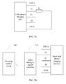
- FIG. 4a shows a schematic structural diagram of another USB charger charging interface.
- the charging interface is a type B USB interface or a Micro USB interface, including 5 pins: VBUS, D-, D+, ID, and GND, where the VBUS pin is a positive pole of an output power supply, and the GND is a negative pole of the output power supply, and different from the embodiment corresponding to FIG. 3a , the detecting resistance R is connected in series between the D+ pin and the GND pin.
- Identification information is an active analog to digital converter.
- FIG. 4b shows a circuit conceptual schematic diagram of another hand held device charging interface corresponding to the USB charger shown in FIG. 4a .
- the difference from the embodiment corresponding to FIG. 3b lies in that: the active analog to digital converter 210 inside the hand held device provided by this embodiment is connected to a D+ pin, and specifically, an input end of the active analog to digital converter 210 is connected to the D+ pin, and an output end of the active analog to digital converter 210 is connected to a charging control circuit 300 inside the hand held device.
- the power supply inside the active analog to digital converter 210 forms a closed loop with the detecting resistance R, and then, the current that flows through the detecting resistance R generates a voltage drop on the detecting resistance R, and the active analog to digital converter 210 acquires the voltage drop on the detecting resistance R, converts a voltage signal on the detecting resistance R to a digital signal and provides it to the charging control circuit 300.
- the charging control circuit 300 compares the acquired voltage drop on the detecting resistance R with the standard voltage range, and when the charging control circuit 300 detects that the voltage drop on the resistance R is within the standard voltage range, an identification signal is output to connect the charging loop of the hand held device and the USB charger, so that the hand held device uses the USB charger for charging; otherwise, the charging control loop 300 outputs that the signal cannot be identified, and the charging loop of the hand held device and the USB charger cannot form a closed loop, that is, the hand held device cannot use the USB charger for charging, thereby ensuring the charging safety of the hand held device.
- the output current of the active analog to digital converter 210 is fixed, and the resistance value of the detecting resistance R is fixed.
- the identification information acquisition module is a passive analog to digital converter and a direct current power supply.
- FIG. 4c shows a schematic structural diagram of another hand held device charging interface that matches the USB charger charging joint shown in FIG. 4a .
- a passive analog to digital converter 220 of the hand held device and a direct current power supply VDD are connected to the D+ pin.
- an input end of the passive analog to digital converter 220 is connected to the D+ pin inside the hand held device charging interface, and an output end of the passive analog to digital converter 220 is connected to the charging control circuit 300 inside the hand held device, and the direct current power supply VDD is connected to the D+ pin of the hand held device charging interface through a pull-up resistance R1.
- the direct current power supply VDD, the pull-up resistance R1, and the detecting resistance R form a closed loop. Then, the current that flows through the detecting resistance R generates a voltage drop on the detecting resistance R, and the passive analog to digital converter 220 acquires the voltage drop on the detecting resistance R, converts the voltage drop to a digital signal and provides it to the charging control circuit 300.
- the charging control circuit 300 compares the acquired voltage drop on the detecting resistance R with the standard voltage range, and when the voltage drop on the detecting resistance R is within the standard voltage range, an identification signal is output to connect the charging loop of the hand held device and the USB charger, so that the hand held device uses the USB charger for charging; otherwise, the charging control loop 300 outputs that the signal cannot be identified, and the charging loop of the hand held device and the USB charger cannot form a closed loop, that is, the hand held device cannot use the USB charger for charging, thereby ensuring the charging safety of the hand held device.
- the figure of the direct current power supply VDD, the resistance value of the pull-up resistance R1, and the resistance value of the detecting resistance R are fixed.
- FIG. 5a shows a schematic structural diagram of a USB charger charging interface.
- the charging interface is a type B USB interface or a Micro USB interface, including 5 pins: VBUS, D-, D+, ID, and GND, where the VBUS pin is a positive pole of an output power supply, and the GND is a negative pole of the output power supply, and different from the embodiment corresponding to FIG. 3a , the detecting resistance R is connected in series between the D- pin and the GND pin.
- the identification information acquisition module is an active analog to digital converter.
- FIG. 5b shows a schematic structural diagram of a hand held device charging interface that matches the USB charger shown in FIG. 5a .
- the active analog to digital converter 210 is connected between a D- pin and a charging control circuit 300.
- the power supply inside the active analog to digital converter forms a closed loop with the detecting resistance R, and then, the current that flows through the detecting resistance R generates a voltage drop on the detecting resistance R, and the active analog to digital converter acquires the voltage drop on the detecting resistance R, converts it to a digital signal and provides it to the charging control circuit 300.
- the charging control circuit 300 compares the acquired voltage drop on the detecting resistance R with a standard voltage range, and when the voltage drop on the detecting resistance R is within the standard voltage range, the hand held device is capable of identifying the USB charger and using the USB charger for charging; otherwise, the USB charger cannot be identified and the USB charger cannot be used for charging either, thereby ensuring the charging safety of the hand held device.
- the output current of the active analog to digital converter 210 is fixed, and the resistance value of the detecting resistance R is fixed.
- the identification information acquisition module is a passive analog to digital converter and a direct current power supply.
- FIG. 5c shows a schematic structural diagram of another hand held device charging interface that matches the USB charger charging joint shown in FIG. 5a .
- a passive analog to digital converter 220 and a direct current power supply VDD are connected to a D-pin.
- an input end of the passive analog to digital converter 220 is connected to the D- pin inside the hand held device charging interface, and an output end of the passive analog to digital converter 220 is connected to the charging control circuit 300 inside the hand held device, and the direct current power supply VDD is connected to the D- pin of the hand held device charging interface through a pull-up resistance R1.
- the direct current power supply VDD, the pull-up resistance R1, and the detecting resistance R connected between the D- pin and the GND pin inside the USB charger form a closed loop. Then, the current that flows through the detecting resistance R generates a voltage drop on the detecting resistance R, and the passive analog to digital converter 220 acquires the voltage drop on the detecting resistance R, converts it to a digital signal and provides it to the charging control circuit 300.
- the charging control circuit 300 compares the acquired voltage drop on the detecting resistance R with the standard voltage range, and when the voltage drop on the detecting resistance R is within the standard voltage range, an identification signal is output to connect the charging loop of the hand held device and the USB charger, so that the hand held device uses the USB charger for charging; otherwise, the charging control loop 300 outputs that the signal cannot be identified, and the charging loop of the hand held device and the USB charger cannot form a closed loop, that is, the hand held device cannot use the USB charger for charging, thereby ensuring the charging safety of the hand held device.
- the figure of the direct current power supply VDD, the resistance value of the pull-up resistance R1, and the resistance value of the detecting resistance R are fixed.
- the identification information module is an identification information memory.
- the identification information memory may be connected to different non-power pins of the USB charger, which will be introduced in the following one by one:
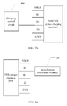
- FIG. 6a shows a schematic structural diagram of a USB charger charging joint.
- the charging joint is a type B USB interface or a Micro USB interface, including 5 pins: VBUS, D-, D+, ID, and GND, where the VBUS pin is a positive pole of an output power supply, and the GND is a negative pole of the output power supply, and different from the embodiment corresponding to FIG. 1 : an identification information module 100 specifically may be the identification information memory 110 that stores identification information of the USB charger.
- the identification information memory 110 is connected to the ID pin, and is configured to store the identification information that identifies identity information of the USB charger, where the identification information may be an 8-bit binary code.
- the identification information memory may be an EPROM (Erasable Programmable ROM, erasable programmable ROM) memory, and certainly it may be other read-write memories.
- FIG. 6b shows a schematic structural diagram of a hand held device charging interface that matches the USB charger charging joint shown in FIG. 6a , where the identification signal acquisition module may be a serial data line.
- the serial data line is connected between the ID pin inside the hand held device and a charging control circuit 300.
- one end of the serial data line is connected to the ID pin inside the hand held device, and the other end is connected to the charging control circuit 300, and is configured to transmit the identification information inside the USB charger into the charging control circuit 300.
- the charging control circuit 300 of the hand held device After the USB charger is inserted into the hand held device charging interface, the charging control circuit 300 of the hand held device acquires the identification information inside the USB charger through the serial data line and compares the identification information with standard identification information, and if the identification information acquired from the USB charger is the same as the standard identification information, an identification signal is output to connect the charging loop of the hand held device and the USB charger, so that the hand held device uses the USB charger for charging; otherwise, the charging control loop 300 outputs that the signal cannot be identified, and the charging loop of the hand held device and the USB charger cannot form a closed loop, that is, the hand held device cannot use the USB charger for charging, thereby ensuring the charging safety of the hand held device.
- the identification code in the USB charger memory may be a code that is set at discretion, and specifically, it may be an 8-bit binary code, and at the same time, the code is stored inside the hand held device.
- the identification information of the USB chargers that matches the hand held devices of the same model may be the same. In this case, the hand held devices of the same model may use the corresponding USB chargers of the same model.
- FIG. 7a shows a schematic structural diagram of another USB charger charging joint.
- the identification information memory 110 which is used to store the identification information of the USB charger, is connected to the D+ pin.
- FIG. 7b shows a schematic structural diagram of a hand held device charging interface that matches the USB charger charging joint shown in FIG. 7a .
- the serial data line is connected between the D+ pin and the charging control circuit 300, and is capable of transmitting the identification information inside the identification information memory 110 to the charging control circuit 300.
- the charging control circuit 300 of the hand held device After the USB charger is inserted into the hand held device charging interface, the charging control circuit 300 of the hand held device acquires the identification information inside the USB charger through the serial data line and compares the identification information with standard identification information, and if the identification information acquired from the USB charger is the same as the standard identification information, an identification signal is output to connect the charging loop of the hand held device and the USB charger, so that the hand held device uses the USB charger for charging; otherwise, the charging control loop 300 outputs that the signal cannot be identified, and the charging loop of the hand held device and the USB charger cannot form a closed loop, that is, the hand held device cannot use the USB charger for charging, thereby ensuring the charging safety of the hand held device.
- FIG. 8a shows another schematic structural diagram of a USB charger charging joint.
- the identification information memory 110 which is used to store the identification information of the USB charger, is connected to the D- pin.
- FIG. 8b shows a schematic structural diagram of a hand held device charging interface that matches the USB charger charging joint shown in FIG. 8a .
- the serial data line is connected between the D- pin and the charging control circuit 300, and is capable of transmitting the identification information inside the identification information memory 110 to the charging control circuit 300.
- the charging control circuit 300 of the hand held device After the USB charger is inserted into the hand held device charging interface, the charging control circuit 300 of the hand held device acquires the identification information inside the USB charger through the serial data line and compares the identification information with standard identification information, and if the identification information acquired from the USB charger is the same as the standard identification information, an identification signal is output to connect the charging loop of the hand held device and the USB charger, so that the hand held device uses the USB charger for charging; otherwise, the charging control loop 300 outputs that the signal cannot be identified, and the charging loop of the hand held device and the USB charger cannot form a closed loop, that is, the hand held device cannot use the USB charger for charging, thereby ensuring the charging safety of the hand held device.
- the identification information memory may be a memory or other storage devices, and the identification information may be a binary code and may also be a code in other coding forms.
- an embodiment of the present invention further provides a method for identifying a universal serial bus interface charger that matches a hand held device, where an identification information acquisition module is added among charging control circuits inside the hand held device, and correspondingly, an identification information module is connected in series inside the USB charger that matches the hand held device, and after the USB charger is inserted into the hand held device charging interface, the method for the hand held device to identify the USB charger includes:
- the identification information may be voltage information on a detecting resistance connected in series inside a USB charger charging joint, and may also be code information.
- S102 Determine whether the identification information is standard identification information. If yes, the hand held device is capable of identifying the USB charger and using the USB charger for charging; otherwise, the hand held device is not capable of identifying the USB charger.
- the identification information may be voltage information, and may also be identification code information, and the following introduces the foregoing two types of identification information in detail, respectively:
- the identification information is voltage information
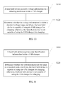
- FIG. 10 shows another method for identifying a USB charger according to an embodiment of the present application, where the identification information inside the USB charger is voltage information, and the identification method includes the following steps:
- the detecting resistance may be connected in series between any non-power pin and a GND pin of the USB charger; an active analog to digital converter is, or a passive analog to digital converter and a direct current power supply are connected to the non-power pin of the hand held device charging interface, which is capable of providing power supply for the detecting resistance and acquiring a voltage drop on the detecting resistance R, and then the voltage drop signal is converted to a digital signal, which is provided to the charging control circuit inside the hand held device.
- the charging control circuit inside the hand held device compares the acquired voltage information on the detecting resistance R with the standard voltage range, and if the voltage information is within the standard voltage range, the charging control circuit is capable of using the USB charger for charging; otherwise, the charging control circuit is not capable of using the USB charger for charging.
- the identification information is an identification code
- FIG. 11 shows a schematic flowchart of another USB charger identification method according to an embodiment of the present application.
- the identification information inside the USB charger is a code that identifies the identity information of the USB charger, where the method includes:
- the identification code inside the USB charger may be an 8-bit binary code, and is configured to exclusively mark an identity of the USB charger.
- the hand held device acquires the identification code through the internal serial data line and provides it to the charging control circuit inside the hand held device.
- the standard code is also an 8-bit binary code.
- the identification code inside the USB charger that matches the hand held device is stored in the charging control circuit inside the hand held device to ensure that the standard code inside the hand held device is the same as the identification code inside the corresponding charger, thereby ensuring that the hand held device can only use its matching USB charger for charging.
- the hand held device mentioned in all embodiments of the present application may be a cell phone.
Landscapes
- Engineering & Computer Science (AREA)
- Theoretical Computer Science (AREA)
- General Engineering & Computer Science (AREA)
- Physics & Mathematics (AREA)
- General Physics & Mathematics (AREA)
- Quality & Reliability (AREA)
- Computer Hardware Design (AREA)
- Power Engineering (AREA)
- Charge And Discharge Circuits For Batteries Or The Like (AREA)
Applications Claiming Priority (1)
| Application Number | Priority Date | Filing Date | Title |
|---|---|---|---|
| PCT/CN2011/078722 WO2011157243A2 (zh) | 2011-08-22 | 2011-08-22 | 手持机、usb充电器及手持机识别usb充电器的方法 |
Publications (3)
| Publication Number | Publication Date |
|---|---|
| EP2713280A2 true EP2713280A2 (de) | 2014-04-02 |
| EP2713280A4 EP2713280A4 (de) | 2014-12-31 |
| EP2713280B1 EP2713280B1 (de) | 2017-02-22 |
Family
ID=45348650
Family Applications (1)
| Application Number | Title | Priority Date | Filing Date |
|---|---|---|---|
| EP11795209.3A Not-in-force EP2713280B1 (de) | 2011-08-22 | 2011-08-22 | Handgeführte vorrichtung, usb-ladegerät und verfahren zur identifizierung des usb-ladegerätes durch die handgeführte vorrichtung |
Country Status (4)
| Country | Link |
|---|---|
| US (1) | US20140103864A1 (de) |
| EP (1) | EP2713280B1 (de) |
| CN (1) | CN102439816B (de) |
| WO (1) | WO2011157243A2 (de) |
Cited By (2)
| Publication number | Priority date | Publication date | Assignee | Title |
|---|---|---|---|---|
| EP2849023A4 (de) * | 2012-05-11 | 2015-09-02 | Fujitsu Ltd | Elektronische vorrichtung und steuerungsverfahren dafür |
| EP3007311A3 (de) * | 2014-10-06 | 2016-05-04 | Samsung Electronics Co., Ltd. | Elektronische vorrichtung und verfahren zur ladung und entladung in elektronischer vorrichtung |
Families Citing this family (26)
| Publication number | Priority date | Publication date | Assignee | Title |
|---|---|---|---|---|
| US9045049B2 (en) * | 2011-08-28 | 2015-06-02 | Irobot Corporation | System and method for in situ charging of a remote vehicle |
| KR20130063131A (ko) * | 2011-12-06 | 2013-06-14 | 삼성전자주식회사 | 터치 감지 파라미터 설정 방법 및 장치 |
| CN202435073U (zh) * | 2011-12-26 | 2012-09-12 | 鸿富锦精密工业(深圳)有限公司 | 充电电池及使用该充电电池的电源系统 |
| TWM445292U (zh) * | 2012-01-03 | 2013-01-11 | Wei-Jin Lin | Usb多用轉接裝置 |
| CN103036276B (zh) * | 2012-11-23 | 2015-03-11 | 小米科技有限责任公司 | 充电器、终端、控制器、系统和充电器识别方法 |
| US20140312691A1 (en) * | 2013-03-15 | 2014-10-23 | Cooper Technologies Company | Smart power strip with automatic device connection detection |
| TWI501085B (zh) * | 2013-05-17 | 2015-09-21 | Primax Electronics Ltd | 通用序列匯流排介面偵測裝置 |
| CN104182021B (zh) * | 2013-05-24 | 2017-05-31 | 快捷半导体(苏州)有限公司 | 一种供电电路、方法及便携式设备 |
| US9582054B2 (en) * | 2013-06-17 | 2017-02-28 | System General Corp. | Method and apparatus for selecting the output of programmable power adapter |
| US9130381B2 (en) * | 2013-08-05 | 2015-09-08 | O2Micro Inc. | Systems and methods for identifying and monitoring a battery charger |
| US10114401B2 (en) * | 2013-11-18 | 2018-10-30 | Infineon Technologies Ag | System and method for a serial bus interface |
| TWI522812B (zh) * | 2014-05-09 | 2016-02-21 | 宏碁股份有限公司 | 通用串列匯流排介面及行動電子裝置 |
| US9564766B2 (en) * | 2014-07-30 | 2017-02-07 | Elwha Llc | Controllable energy transfer between portable devices |
| CN104767180B (zh) * | 2015-03-20 | 2018-06-08 | 深圳市万普拉斯科技有限公司 | Usb接口大电流充电保护方法和系统 |
| CN106374309B (zh) * | 2016-11-02 | 2020-12-11 | 上海传英信息技术有限公司 | Usb传输线、移动终端及usb充电方法 |
| US11264822B2 (en) | 2016-11-29 | 2022-03-01 | Huawei Technologies Co., Ltd. | Method for determining charger, related device, and system |
| CN107069869A (zh) * | 2017-04-27 | 2017-08-18 | 北京小米移动软件有限公司 | 电子设备 |
| JP6882934B2 (ja) * | 2017-05-12 | 2021-06-02 | Dynabook株式会社 | 電子機器および方法 |
| US10237381B2 (en) | 2017-07-13 | 2019-03-19 | Sorenson Ip Holdings, Llc | Telephone receiver identification |
| WO2020024335A1 (zh) * | 2018-08-03 | 2020-02-06 | 李宗谕 | 民用飞机客舱内供电方法 |
| KR102714346B1 (ko) * | 2018-09-03 | 2024-10-10 | 삼성전자주식회사 | 전력 정보에 기반하여 외부 전자 장치를 식별하는 방법, 이를 지원하는 전자 장치 및 저장 매체 |
| CN109193870A (zh) * | 2018-11-07 | 2019-01-11 | 深圳市云雄能源管理有限公司 | 一种电池充电管理方法及装置 |
| US11100255B1 (en) * | 2019-07-01 | 2021-08-24 | Dialog Semiconductor (Uk) Limited | Method and apparatus for high voltage protection |
| CN114465323B (zh) * | 2022-02-28 | 2026-01-06 | 杭州中赣电子科技有限公司 | 一种充电保护方法、受电设备及充电设备 |
| CN114614551B (zh) * | 2022-05-11 | 2022-08-02 | 北京拿云致象科技发展有限公司 | 一种充电电瓶 |
| CN120067009B (zh) * | 2024-12-31 | 2026-01-30 | 中国船舶集团有限公司第七一六研究所 | 一种嵌入式系统usb孤儿设备的类驱动重枚举方法 |
Family Cites Families (9)
| Publication number | Priority date | Publication date | Assignee | Title |
|---|---|---|---|---|
| KR200275514Y1 (ko) * | 2002-02-15 | 2002-05-11 | 신형범 | 충전지를 내장한 휴대용 충전장치 |
| US7271568B2 (en) * | 2004-02-11 | 2007-09-18 | Research In Motion Limited | Battery charger for portable devices and related methods |
| US20080265838A1 (en) * | 2007-04-24 | 2008-10-30 | Saurabh Garg | Battery charging using a USB-ID pin of a USB interface |
| KR20090028196A (ko) * | 2007-09-14 | 2009-03-18 | 삼성전자주식회사 | 휴대 단말기의 충전 장치 및 방법 |
| US20100070659A1 (en) * | 2008-09-17 | 2010-03-18 | Kenneth Ma | Method and system for operating and/or charging a battery powered usb device based on a usb port type |
| CN101398459B (zh) * | 2008-10-28 | 2011-02-09 | 华为终端有限公司 | 识别充电器类型的方法及装置 |
| TWM357713U (en) * | 2008-12-10 | 2009-05-21 | Inventec Besta Co Ltd | Electronic apparatus charged through USB connection and related USB charging device |
| KR101579146B1 (ko) * | 2009-02-27 | 2015-12-21 | 페어차일드 세미컨덕터 코포레이션 | 주변 장치 호스트 충전 |
| CN101901201B (zh) * | 2010-08-06 | 2014-07-16 | 中兴通讯股份有限公司 | 一种在电子设备上实现usb otg功能的方法和装置 |
-
2011
- 2011-08-22 WO PCT/CN2011/078722 patent/WO2011157243A2/zh not_active Ceased
- 2011-08-22 EP EP11795209.3A patent/EP2713280B1/de not_active Not-in-force
- 2011-08-22 CN CN201180001373.5A patent/CN102439816B/zh active Active
-
2013
- 2013-12-18 US US14/133,223 patent/US20140103864A1/en not_active Abandoned
Cited By (3)
| Publication number | Priority date | Publication date | Assignee | Title |
|---|---|---|---|---|
| EP2849023A4 (de) * | 2012-05-11 | 2015-09-02 | Fujitsu Ltd | Elektronische vorrichtung und steuerungsverfahren dafür |
| EP3007311A3 (de) * | 2014-10-06 | 2016-05-04 | Samsung Electronics Co., Ltd. | Elektronische vorrichtung und verfahren zur ladung und entladung in elektronischer vorrichtung |
| US9960616B2 (en) | 2014-10-06 | 2018-05-01 | Samsung Electronics Co., Ltd. | Electronic device and method for charging and discharging in electronic device |
Also Published As
| Publication number | Publication date |
|---|---|
| WO2011157243A2 (zh) | 2011-12-22 |
| US20140103864A1 (en) | 2014-04-17 |
| EP2713280B1 (de) | 2017-02-22 |
| CN102439816A (zh) | 2012-05-02 |
| CN102439816B (zh) | 2015-01-21 |
| WO2011157243A3 (zh) | 2012-02-09 |
| EP2713280A4 (de) | 2014-12-31 |
Similar Documents
| Publication | Publication Date | Title |
|---|---|---|
| EP2713280A2 (de) | Handgeführte vorrichtung, usb-ladegerät und verfahren zur identifizierung des usb-ladegerätes durch die handgeführte vorrichtung | |
| CN101398459B (zh) | 识别充电器类型的方法及装置 | |
| US20080272741A1 (en) | Systems and methods for detecting power sources | |
| JP5388484B2 (ja) | 電源を検出するための装置および方法 | |
| US8683087B2 (en) | Mobile device auto detection apparatus and method | |
| US8970165B2 (en) | Determination circuit | |
| CN1881738B (zh) | 充电模式控制电路及方法 | |
| CN103259300B (zh) | 便携式电子装置以及其充电方法 | |
| CN104272216A (zh) | 电子设备及其控制方法 | |
| CN102694400B (zh) | 输入输出电路 | |
| CN104882924B (zh) | 充电识别设备及其识别方法 | |
| CN103064489A (zh) | 一种根据usb接口状态进行内部电路选择的方法及终端 | |
| US20140070791A1 (en) | Electronic device and method of electronic device for determining power source device | |
| US20220222063A1 (en) | Portable device communicating with charger and operating method thereof | |
| WO2008090378A1 (en) | Battery connection unit | |
| US10141760B2 (en) | Power supply circuit, charge circuit, charging system, power supplying method, and charging method | |
| CN103217650A (zh) | 电池类型检测方法及采用该方法设计的移动终端 | |
| CN104659867A (zh) | 电源装置及调变便携式装置的电源装置充电电流的方法 | |
| JP7739788B2 (ja) | 制御装置及び充電システム | |
| CN206099470U (zh) | 用于快速充电器的转换装置 | |
| EP2530807B1 (de) | Elektrische Vorrichtung und Verifizierungsverfahren eines dafür vorgesehenen Batteriemoduls | |
| JP6922291B2 (ja) | 制御装置、受電装置、受電用制御システム、電子機器及び無接点電力伝送システム | |
| CN210742885U (zh) | 笔记本电池管理装置 | |
| JP2012104039A (ja) | 電子機器、電池パックおよび通信システムならびに通信方法 | |
| CN117096991A (zh) | 一种充电方法、电子设备及可读存储介质 |
Legal Events
| Date | Code | Title | Description |
|---|---|---|---|
| PUAI | Public reference made under article 153(3) epc to a published international application that has entered the european phase |
Free format text: ORIGINAL CODE: 0009012 |
|
| 17P | Request for examination filed |
Effective date: 20131218 |
|
| AK | Designated contracting states |
Kind code of ref document: A2 Designated state(s): AL AT BE BG CH CY CZ DE DK EE ES FI FR GB GR HR HU IE IS IT LI LT LU LV MC MK MT NL NO PL PT RO RS SE SI SK SM TR |
|
| DAX | Request for extension of the european patent (deleted) | ||
| A4 | Supplementary search report drawn up and despatched |
Effective date: 20141203 |
|
| RIC1 | Information provided on ipc code assigned before grant |
Ipc: G06F 13/38 20060101AFI20141127BHEP Ipc: G06F 13/40 20060101ALI20141127BHEP Ipc: G06F 1/26 20060101ALI20141127BHEP |
|
| 17Q | First examination report despatched |
Effective date: 20160303 |
|
| GRAP | Despatch of communication of intention to grant a patent |
Free format text: ORIGINAL CODE: EPIDOSNIGR1 |
|
| INTG | Intention to grant announced |
Effective date: 20160907 |
|
| GRAS | Grant fee paid |
Free format text: ORIGINAL CODE: EPIDOSNIGR3 |
|
| GRAA | (expected) grant |
Free format text: ORIGINAL CODE: 0009210 |
|
| AK | Designated contracting states |
Kind code of ref document: B1 Designated state(s): AL AT BE BG CH CY CZ DE DK EE ES FI FR GB GR HR HU IE IS IT LI LT LU LV MC MK MT NL NO PL PT RO RS SE SI SK SM TR |
|
| REG | Reference to a national code |
Ref country code: GB Ref legal event code: FG4D |
|
| REG | Reference to a national code |
Ref country code: CH Ref legal event code: EP |
|
| REG | Reference to a national code |
Ref country code: AT Ref legal event code: REF Ref document number: 869762 Country of ref document: AT Kind code of ref document: T Effective date: 20170315 |
|
| REG | Reference to a national code |
Ref country code: IE Ref legal event code: FG4D |
|
| REG | Reference to a national code |
Ref country code: DE Ref legal event code: R096 Ref document number: 602011035251 Country of ref document: DE |
|
| REG | Reference to a national code |
Ref country code: LT Ref legal event code: MG4D |
|
| REG | Reference to a national code |
Ref country code: NL Ref legal event code: MP Effective date: 20170222 |
|
| REG | Reference to a national code |
Ref country code: FR Ref legal event code: PLFP Year of fee payment: 7 |
|
| REG | Reference to a national code |
Ref country code: AT Ref legal event code: MK05 Ref document number: 869762 Country of ref document: AT Kind code of ref document: T Effective date: 20170222 |
|
| PG25 | Lapsed in a contracting state [announced via postgrant information from national office to epo] |
Ref country code: GR Free format text: LAPSE BECAUSE OF FAILURE TO SUBMIT A TRANSLATION OF THE DESCRIPTION OR TO PAY THE FEE WITHIN THE PRESCRIBED TIME-LIMIT Effective date: 20170523 Ref country code: FI Free format text: LAPSE BECAUSE OF FAILURE TO SUBMIT A TRANSLATION OF THE DESCRIPTION OR TO PAY THE FEE WITHIN THE PRESCRIBED TIME-LIMIT Effective date: 20170222 Ref country code: HR Free format text: LAPSE BECAUSE OF FAILURE TO SUBMIT A TRANSLATION OF THE DESCRIPTION OR TO PAY THE FEE WITHIN THE PRESCRIBED TIME-LIMIT Effective date: 20170222 Ref country code: NO Free format text: LAPSE BECAUSE OF FAILURE TO SUBMIT A TRANSLATION OF THE DESCRIPTION OR TO PAY THE FEE WITHIN THE PRESCRIBED TIME-LIMIT Effective date: 20170522 Ref country code: LT Free format text: LAPSE BECAUSE OF FAILURE TO SUBMIT A TRANSLATION OF THE DESCRIPTION OR TO PAY THE FEE WITHIN THE PRESCRIBED TIME-LIMIT Effective date: 20170222 |
|
| PG25 | Lapsed in a contracting state [announced via postgrant information from national office to epo] |
Ref country code: ES Free format text: LAPSE BECAUSE OF FAILURE TO SUBMIT A TRANSLATION OF THE DESCRIPTION OR TO PAY THE FEE WITHIN THE PRESCRIBED TIME-LIMIT Effective date: 20170222 Ref country code: AT Free format text: LAPSE BECAUSE OF FAILURE TO SUBMIT A TRANSLATION OF THE DESCRIPTION OR TO PAY THE FEE WITHIN THE PRESCRIBED TIME-LIMIT Effective date: 20170222 Ref country code: BG Free format text: LAPSE BECAUSE OF FAILURE TO SUBMIT A TRANSLATION OF THE DESCRIPTION OR TO PAY THE FEE WITHIN THE PRESCRIBED TIME-LIMIT Effective date: 20170522 Ref country code: PT Free format text: LAPSE BECAUSE OF FAILURE TO SUBMIT A TRANSLATION OF THE DESCRIPTION OR TO PAY THE FEE WITHIN THE PRESCRIBED TIME-LIMIT Effective date: 20170622 Ref country code: NL Free format text: LAPSE BECAUSE OF FAILURE TO SUBMIT A TRANSLATION OF THE DESCRIPTION OR TO PAY THE FEE WITHIN THE PRESCRIBED TIME-LIMIT Effective date: 20170222 Ref country code: LV Free format text: LAPSE BECAUSE OF FAILURE TO SUBMIT A TRANSLATION OF THE DESCRIPTION OR TO PAY THE FEE WITHIN THE PRESCRIBED TIME-LIMIT Effective date: 20170222 Ref country code: RS Free format text: LAPSE BECAUSE OF FAILURE TO SUBMIT A TRANSLATION OF THE DESCRIPTION OR TO PAY THE FEE WITHIN THE PRESCRIBED TIME-LIMIT Effective date: 20170222 Ref country code: SE Free format text: LAPSE BECAUSE OF FAILURE TO SUBMIT A TRANSLATION OF THE DESCRIPTION OR TO PAY THE FEE WITHIN THE PRESCRIBED TIME-LIMIT Effective date: 20170222 |
|
| PG25 | Lapsed in a contracting state [announced via postgrant information from national office to epo] |
Ref country code: IT Free format text: LAPSE BECAUSE OF FAILURE TO SUBMIT A TRANSLATION OF THE DESCRIPTION OR TO PAY THE FEE WITHIN THE PRESCRIBED TIME-LIMIT Effective date: 20170222 Ref country code: SK Free format text: LAPSE BECAUSE OF FAILURE TO SUBMIT A TRANSLATION OF THE DESCRIPTION OR TO PAY THE FEE WITHIN THE PRESCRIBED TIME-LIMIT Effective date: 20170222 Ref country code: EE Free format text: LAPSE BECAUSE OF FAILURE TO SUBMIT A TRANSLATION OF THE DESCRIPTION OR TO PAY THE FEE WITHIN THE PRESCRIBED TIME-LIMIT Effective date: 20170222 Ref country code: RO Free format text: LAPSE BECAUSE OF FAILURE TO SUBMIT A TRANSLATION OF THE DESCRIPTION OR TO PAY THE FEE WITHIN THE PRESCRIBED TIME-LIMIT Effective date: 20170222 Ref country code: CZ Free format text: LAPSE BECAUSE OF FAILURE TO SUBMIT A TRANSLATION OF THE DESCRIPTION OR TO PAY THE FEE WITHIN THE PRESCRIBED TIME-LIMIT Effective date: 20170222 |
|
| REG | Reference to a national code |
Ref country code: DE Ref legal event code: R097 Ref document number: 602011035251 Country of ref document: DE |
|
| PG25 | Lapsed in a contracting state [announced via postgrant information from national office to epo] |
Ref country code: SM Free format text: LAPSE BECAUSE OF FAILURE TO SUBMIT A TRANSLATION OF THE DESCRIPTION OR TO PAY THE FEE WITHIN THE PRESCRIBED TIME-LIMIT Effective date: 20170222 Ref country code: PL Free format text: LAPSE BECAUSE OF FAILURE TO SUBMIT A TRANSLATION OF THE DESCRIPTION OR TO PAY THE FEE WITHIN THE PRESCRIBED TIME-LIMIT Effective date: 20170222 Ref country code: DK Free format text: LAPSE BECAUSE OF FAILURE TO SUBMIT A TRANSLATION OF THE DESCRIPTION OR TO PAY THE FEE WITHIN THE PRESCRIBED TIME-LIMIT Effective date: 20170222 |
|
| PLBE | No opposition filed within time limit |
Free format text: ORIGINAL CODE: 0009261 |
|
| STAA | Information on the status of an ep patent application or granted ep patent |
Free format text: STATUS: NO OPPOSITION FILED WITHIN TIME LIMIT |
|
| 26N | No opposition filed |
Effective date: 20171123 |
|
| PG25 | Lapsed in a contracting state [announced via postgrant information from national office to epo] |
Ref country code: SI Free format text: LAPSE BECAUSE OF FAILURE TO SUBMIT A TRANSLATION OF THE DESCRIPTION OR TO PAY THE FEE WITHIN THE PRESCRIBED TIME-LIMIT Effective date: 20170222 |
|
| REG | Reference to a national code |
Ref country code: CH Ref legal event code: PL |
|
| PG25 | Lapsed in a contracting state [announced via postgrant information from national office to epo] |
Ref country code: MC Free format text: LAPSE BECAUSE OF FAILURE TO SUBMIT A TRANSLATION OF THE DESCRIPTION OR TO PAY THE FEE WITHIN THE PRESCRIBED TIME-LIMIT Effective date: 20170222 |
|
| PG25 | Lapsed in a contracting state [announced via postgrant information from national office to epo] |
Ref country code: CH Free format text: LAPSE BECAUSE OF NON-PAYMENT OF DUE FEES Effective date: 20170831 Ref country code: LI Free format text: LAPSE BECAUSE OF NON-PAYMENT OF DUE FEES Effective date: 20170831 |
|
| REG | Reference to a national code |
Ref country code: IE Ref legal event code: MM4A |
|
| REG | Reference to a national code |
Ref country code: BE Ref legal event code: MM Effective date: 20170831 |
|
| PG25 | Lapsed in a contracting state [announced via postgrant information from national office to epo] |
Ref country code: LU Free format text: LAPSE BECAUSE OF NON-PAYMENT OF DUE FEES Effective date: 20170822 |
|
| REG | Reference to a national code |
Ref country code: FR Ref legal event code: PLFP Year of fee payment: 8 |
|
| PG25 | Lapsed in a contracting state [announced via postgrant information from national office to epo] |
Ref country code: IE Free format text: LAPSE BECAUSE OF NON-PAYMENT OF DUE FEES Effective date: 20170822 |
|
| PG25 | Lapsed in a contracting state [announced via postgrant information from national office to epo] |
Ref country code: BE Free format text: LAPSE BECAUSE OF NON-PAYMENT OF DUE FEES Effective date: 20170831 |
|
| PG25 | Lapsed in a contracting state [announced via postgrant information from national office to epo] |
Ref country code: MT Free format text: LAPSE BECAUSE OF NON-PAYMENT OF DUE FEES Effective date: 20170822 |
|
| REG | Reference to a national code |
Ref country code: DE Ref legal event code: R081 Ref document number: 602011035251 Country of ref document: DE Owner name: HUAWEI DEVICE CO., LTD., DONGGUAN, CN Free format text: FORMER OWNER: HUAWEI DEVICE CO., LTD., SHENZHEN, GUANGDONG, CN |
|
| REG | Reference to a national code |
Ref country code: GB Ref legal event code: 732E Free format text: REGISTERED BETWEEN 20190124 AND 20190130 |
|
| PG25 | Lapsed in a contracting state [announced via postgrant information from national office to epo] |
Ref country code: HU Free format text: LAPSE BECAUSE OF FAILURE TO SUBMIT A TRANSLATION OF THE DESCRIPTION OR TO PAY THE FEE WITHIN THE PRESCRIBED TIME-LIMIT; INVALID AB INITIO Effective date: 20110822 |
|
| PG25 | Lapsed in a contracting state [announced via postgrant information from national office to epo] |
Ref country code: CY Free format text: LAPSE BECAUSE OF NON-PAYMENT OF DUE FEES Effective date: 20170222 |
|
| PG25 | Lapsed in a contracting state [announced via postgrant information from national office to epo] |
Ref country code: MK Free format text: LAPSE BECAUSE OF FAILURE TO SUBMIT A TRANSLATION OF THE DESCRIPTION OR TO PAY THE FEE WITHIN THE PRESCRIBED TIME-LIMIT Effective date: 20170222 |
|
| PG25 | Lapsed in a contracting state [announced via postgrant information from national office to epo] |
Ref country code: TR Free format text: LAPSE BECAUSE OF FAILURE TO SUBMIT A TRANSLATION OF THE DESCRIPTION OR TO PAY THE FEE WITHIN THE PRESCRIBED TIME-LIMIT Effective date: 20170222 |
|
| PG25 | Lapsed in a contracting state [announced via postgrant information from national office to epo] |
Ref country code: AL Free format text: LAPSE BECAUSE OF FAILURE TO SUBMIT A TRANSLATION OF THE DESCRIPTION OR TO PAY THE FEE WITHIN THE PRESCRIBED TIME-LIMIT Effective date: 20170222 Ref country code: IS Free format text: LAPSE BECAUSE OF FAILURE TO SUBMIT A TRANSLATION OF THE DESCRIPTION OR TO PAY THE FEE WITHIN THE PRESCRIBED TIME-LIMIT Effective date: 20170622 |
|
| PGFP | Annual fee paid to national office [announced via postgrant information from national office to epo] |
Ref country code: GB Payment date: 20230629 Year of fee payment: 13 |
|
| PGFP | Annual fee paid to national office [announced via postgrant information from national office to epo] |
Ref country code: FR Payment date: 20230703 Year of fee payment: 13 Ref country code: DE Payment date: 20230703 Year of fee payment: 13 |
|
| REG | Reference to a national code |
Ref country code: DE Ref legal event code: R119 Ref document number: 602011035251 Country of ref document: DE |
|
| GBPC | Gb: european patent ceased through non-payment of renewal fee |
Effective date: 20240822 |
|
| PG25 | Lapsed in a contracting state [announced via postgrant information from national office to epo] |
Ref country code: DE Free format text: LAPSE BECAUSE OF NON-PAYMENT OF DUE FEES Effective date: 20250301 |
|
| PG25 | Lapsed in a contracting state [announced via postgrant information from national office to epo] |
Ref country code: GB Free format text: LAPSE BECAUSE OF NON-PAYMENT OF DUE FEES Effective date: 20240822 |
|
| PG25 | Lapsed in a contracting state [announced via postgrant information from national office to epo] |
Ref country code: FR Free format text: LAPSE BECAUSE OF NON-PAYMENT OF DUE FEES Effective date: 20240831 |