EP2713357A1 - Led-videobildschirm - Google Patents
Led-videobildschirm Download PDFInfo
- Publication number
- EP2713357A1 EP2713357A1 EP11856909.4A EP11856909A EP2713357A1 EP 2713357 A1 EP2713357 A1 EP 2713357A1 EP 11856909 A EP11856909 A EP 11856909A EP 2713357 A1 EP2713357 A1 EP 2713357A1
- Authority
- EP
- European Patent Office
- Prior art keywords
- leds
- constant current
- led
- pulse width
- same
- Prior art date
- Legal status (The legal status is an assumption and is not a legal conclusion. Google has not performed a legal analysis and makes no representation as to the accuracy of the status listed.)
- Withdrawn
Links
- 238000004891 communication Methods 0.000 claims description 19
- 238000012937 correction Methods 0.000 claims description 11
- 238000005259 measurement Methods 0.000 claims description 11
- 239000011159 matrix material Substances 0.000 claims description 9
- 230000005540 biological transmission Effects 0.000 claims description 7
- 230000007246 mechanism Effects 0.000 claims description 7
- 238000012546 transfer Methods 0.000 claims description 7
- 230000004438 eyesight Effects 0.000 claims description 5
- 238000003860 storage Methods 0.000 claims description 5
- 238000001514 detection method Methods 0.000 claims description 2
- 238000012544 monitoring process Methods 0.000 claims 1
- 238000000034 method Methods 0.000 description 24
- 230000001965 increasing effect Effects 0.000 description 18
- 238000010586 diagram Methods 0.000 description 17
- 230000008569 process Effects 0.000 description 13
- 238000004519 manufacturing process Methods 0.000 description 11
- 239000004020 conductor Substances 0.000 description 10
- 238000009826 distribution Methods 0.000 description 10
- 230000008901 benefit Effects 0.000 description 9
- 230000007704 transition Effects 0.000 description 9
- 238000009434 installation Methods 0.000 description 5
- 230000009467 reduction Effects 0.000 description 5
- 230000000694 effects Effects 0.000 description 4
- 238000012545 processing Methods 0.000 description 4
- 230000006870 function Effects 0.000 description 3
- 230000009471 action Effects 0.000 description 2
- 230000004913 activation Effects 0.000 description 2
- 230000004075 alteration Effects 0.000 description 2
- 238000013459 approach Methods 0.000 description 2
- 230000006399 behavior Effects 0.000 description 2
- 239000003086 colorant Substances 0.000 description 2
- 230000009849 deactivation Effects 0.000 description 2
- 238000013461 design Methods 0.000 description 2
- 230000010354 integration Effects 0.000 description 2
- 230000004048 modification Effects 0.000 description 2
- 238000012986 modification Methods 0.000 description 2
- 238000005457 optimization Methods 0.000 description 2
- 230000004044 response Effects 0.000 description 2
- 230000001360 synchronised effect Effects 0.000 description 2
- 239000000872 buffer Substances 0.000 description 1
- 239000002775 capsule Substances 0.000 description 1
- 238000010276 construction Methods 0.000 description 1
- 230000001276 controlling effect Effects 0.000 description 1
- 230000006837 decompression Effects 0.000 description 1
- 230000007547 defect Effects 0.000 description 1
- 238000005516 engineering process Methods 0.000 description 1
- 238000000605 extraction Methods 0.000 description 1
- 230000006872 improvement Effects 0.000 description 1
- 230000001939 inductive effect Effects 0.000 description 1
- 238000009776 industrial production Methods 0.000 description 1
- 238000003780 insertion Methods 0.000 description 1
- 230000037431 insertion Effects 0.000 description 1
- 230000001105 regulatory effect Effects 0.000 description 1
- 238000000926 separation method Methods 0.000 description 1
- 238000012360 testing method Methods 0.000 description 1
- 230000016776 visual perception Effects 0.000 description 1
- 230000002747 voluntary effect Effects 0.000 description 1
Images











Classifications
-
- G—PHYSICS
- G09—EDUCATION; CRYPTOGRAPHY; DISPLAY; ADVERTISING; SEALS
- G09G—ARRANGEMENTS OR CIRCUITS FOR CONTROL OF INDICATING DEVICES USING STATIC MEANS TO PRESENT VARIABLE INFORMATION
- G09G3/00—Control arrangements or circuits, of interest only in connection with visual indicators other than cathode-ray tubes
- G09G3/20—Control arrangements or circuits, of interest only in connection with visual indicators other than cathode-ray tubes for presentation of an assembly of a number of characters, e.g. a page, by composing the assembly by combination of individual elements arranged in a matrix no fixed position being assigned to or needed to be assigned to the individual characters or partial characters
- G09G3/22—Control arrangements or circuits, of interest only in connection with visual indicators other than cathode-ray tubes for presentation of an assembly of a number of characters, e.g. a page, by composing the assembly by combination of individual elements arranged in a matrix no fixed position being assigned to or needed to be assigned to the individual characters or partial characters using controlled light sources
- G09G3/30—Control arrangements or circuits, of interest only in connection with visual indicators other than cathode-ray tubes for presentation of an assembly of a number of characters, e.g. a page, by composing the assembly by combination of individual elements arranged in a matrix no fixed position being assigned to or needed to be assigned to the individual characters or partial characters using controlled light sources using electroluminescent panels
- G09G3/32—Control arrangements or circuits, of interest only in connection with visual indicators other than cathode-ray tubes for presentation of an assembly of a number of characters, e.g. a page, by composing the assembly by combination of individual elements arranged in a matrix no fixed position being assigned to or needed to be assigned to the individual characters or partial characters using controlled light sources using electroluminescent panels semiconductive, e.g. using light-emitting diodes [LED]
-
- G—PHYSICS
- G09—EDUCATION; CRYPTOGRAPHY; DISPLAY; ADVERTISING; SEALS
- G09G—ARRANGEMENTS OR CIRCUITS FOR CONTROL OF INDICATING DEVICES USING STATIC MEANS TO PRESENT VARIABLE INFORMATION
- G09G5/00—Control arrangements or circuits for visual indicators common to cathode-ray tube indicators and other visual indicators
- G09G5/003—Details of a display terminal, the details relating to the control arrangement of the display terminal and to the interfaces thereto
-
- H—ELECTRICITY
- H05—ELECTRIC TECHNIQUES NOT OTHERWISE PROVIDED FOR
- H05B—ELECTRIC HEATING; ELECTRIC LIGHT SOURCES NOT OTHERWISE PROVIDED FOR; CIRCUIT ARRANGEMENTS FOR ELECTRIC LIGHT SOURCES, IN GENERAL
- H05B45/00—Circuit arrangements for operating light-emitting diodes [LED]
- H05B45/20—Controlling the colour of the light
-
- H—ELECTRICITY
- H05—ELECTRIC TECHNIQUES NOT OTHERWISE PROVIDED FOR
- H05B—ELECTRIC HEATING; ELECTRIC LIGHT SOURCES NOT OTHERWISE PROVIDED FOR; CIRCUIT ARRANGEMENTS FOR ELECTRIC LIGHT SOURCES, IN GENERAL
- H05B45/00—Circuit arrangements for operating light-emitting diodes [LED]
- H05B45/30—Driver circuits
- H05B45/37—Converter circuits
-
- G—PHYSICS
- G09—EDUCATION; CRYPTOGRAPHY; DISPLAY; ADVERTISING; SEALS
- G09G—ARRANGEMENTS OR CIRCUITS FOR CONTROL OF INDICATING DEVICES USING STATIC MEANS TO PRESENT VARIABLE INFORMATION
- G09G2320/00—Control of display operating conditions
- G09G2320/06—Adjustment of display parameters
- G09G2320/0666—Adjustment of display parameters for control of colour parameters, e.g. colour temperature
-
- H—ELECTRICITY
- H05—ELECTRIC TECHNIQUES NOT OTHERWISE PROVIDED FOR
- H05B—ELECTRIC HEATING; ELECTRIC LIGHT SOURCES NOT OTHERWISE PROVIDED FOR; CIRCUIT ARRANGEMENTS FOR ELECTRIC LIGHT SOURCES, IN GENERAL
- H05B45/00—Circuit arrangements for operating light-emitting diodes [LED]
- H05B45/30—Driver circuits
- H05B45/395—Linear regulators
-
- H—ELECTRICITY
- H05—ELECTRIC TECHNIQUES NOT OTHERWISE PROVIDED FOR
- H05B—ELECTRIC HEATING; ELECTRIC LIGHT SOURCES NOT OTHERWISE PROVIDED FOR; CIRCUIT ARRANGEMENTS FOR ELECTRIC LIGHT SOURCES, IN GENERAL
- H05B45/00—Circuit arrangements for operating light-emitting diodes [LED]
- H05B45/40—Details of LED load circuits
- H05B45/44—Details of LED load circuits with an active control inside an LED matrix
- H05B45/48—Details of LED load circuits with an active control inside an LED matrix having LEDs organised in strings and incorporating parallel shunting devices
Definitions
- This invention is about a light-emitting diode (LED) video display including several functional units which comprise interconnected modules forming a two-dimensional regular matrix, each module including in turn a number of pixels.
- the final objective is to provide a solution to the three main problems associated with this type of device: to reduce power supply, obtain the appropriate energy performance and achieve integration of the electronic system into a single and flexible printed circuit.
- the suggested solution features additionally high adaptability when providing valid solutions to volatile technological variables or different design issues, such as supply voltage, number of pixels per module, number of LEDs per pixel, or live voltage drops and their relative light intensity.
- the invention also makes it possible to implement modules through integrated circuits where the whole main electronic system has been installed (except for LED diodes), so that displays are only made up of an association of integrated circuits and LEDs mounted on a printed circuit which is preferably flexible but may also be rigid, thus simplifying and reducing the manufacturing price of this type of display.
- the resulting displays have extremely reduced thickness and weight, which represents a key factor in their easy installation in locations where it is technically complicated or impossible to install current LED displays.
- LED video displays made of a regular matrix of LED diodes are well known. These displays are the most efficient mechanism for the manufacture of larger displays.
- LED video displays are implemented by following the same general guidelines. They are physically installed in special cabinets, so that LED panels are installed in the front and the whole electronic system required for its operation is protected inside.
- Several supply sources generate one or different low-tension voltages from the power supply.
- the circuitry normally made up by integrated analogue drivers, controls the brightness of each LED.
- a specific digital electronic control regulates transmission and generation of images on the display.
- the difficulty in implementing flexible video displays resides, firstly, in the integration of the electronic system required, including LEDs themselves, into a very small profile, typically a single printed circuit. Basically, this electronic system shall be able to individually control the brightness of each LED. Secondly, the implementation of the analogue driver shall be such that the power supply required for its correct operation is sufficiently reduced to be efficiently transported throughout its entire length and width. It shall be considered that, to solve this problem, dc/dc converters cannot be introduced into the reduced profiles that flexible video displays require nor can large section conductors be used to transport these currents.
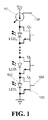
- the controller or source of constant current 101 supplies constant current to all LEDs 102.
- Each LED turns on and off by means of MOS 103 transistors connected in parallel to each diode and applying a specific voltage in their gate terminal 104.
- the source of constant current has a 105 control input, which allows interruption of this current when all LEDs are off, thus reducing consumption.
- the total current consumed by this driver and the N LEDs connected in series is equal to the current consumed by only one LED.
- the number of LEDs that can be connected in series for a driver like the one shown in figure 1 is limited in practice by the maximum gate-supply voltage of transistors.
- the sum of all LED live voltages, in a worst-case scenario, shall be such that voltage at the transistor gate does not exceed that maximum value under any circumstances.
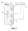
- analogue driver is the one shown in figure 2 , generally implemented in integrated circuits controlling 201 N LEDs which are connected through N outputs; for that purpose, they use N sources of 202 constant current which may be turned on or off externally by means of a suitable digital 203 interface.
- These analogue drivers do not comprise the other digital electronics in charge of generating digital modulations which independently control or adjust the brightness of each LED or other functions related to the generation or processing of images from the digital domain.
- the total current consumed by this driver and the N LEDs is equal to the sum of all the individual currents consumed by each of the LEDs and the driver itself.
- the number of LEDs that can be controlled by a driver such as the one shown in figure 2 is limited by the section of the conductors required to transport the currents consumed by them. This fact makes it necessary to use dc/dc converters or ac/dc power supplies for each group of LEDs, in order to reduce these currents and increase the supply voltage.
- each module includes the necessary circuits - both digital and analogue - to implement flexible LED displays.
- pulse width modulation techniques used to control the brightness of each LED are well know.
- this invention comprises many pixels forming a matrix, each pixel being made up of a non-zero number of red LED L R diodes, a non-zero number of green LED L G diodes and a non-zero number of blue LED L B diodes; they include a digital network aimed to regulate transmission and generation of images on the display.
- the main novelty of this invention is that it comprises diversity of functional units arranged according to a regular two-dimensional matrix connected through the digital network in order to distribute numerical information about image contents among the said functional units.
- Each functional unit also comprises the following elements:
- display there are circuits of LEDs of the same colour connected in series, in such a way that there is a first set of constant current sources where each constant current source is only applied to red LEDs, a second set of constant current sources where each constant current source is only applied to green LEDs and a third set of constant current sources where each constant current source is only applied to blue LEDs, resulting in an independent consumption by each colour and a physical distribution of the said elements into different modules with flexible interconnections, each of them including N pixels and incorporating the necessary electronics, both digital and analogue, to completely control the functioning of the display.
- each module is physically arranged into a group of modules, each of them comprising the same number of pixels, the said modules being electrically interconnected by means of flexible or rigid unions provided with the connections forming the circuits of LEDs connected in series and with the constant current sources shared by the group of modules.
- Each module also comprising:
- each module incorporates a set of N ⁇ (L R +L G +L B ) analogue switches connected in parallel to each and every one of the LEDs.
- These analogue switches may be implemented by a NMOS, PMOS, PNP, NPN transistor or any valid combination of them, for instance two-way gateways (T-gates), or by any other device governed by a control inlet which allows voluntary interruption of electrical current passage.
- each N ⁇ (L R +L G +L B ) analogue switch incorporates a level adapter, in such a way that every switch is regulated by the same number of digital control signals as those that form the digital network; those adapters allow independent activation or deactivation of each and every analogue switch and, therefore, the individual switching on and off of each LED in the same module may be controlled from the digital domain.
- each pixel forming the display is made up by three LEDs with primary colours.
- one of the LEDs is replaced by a circuit of two LEDs of the same colour in series in order to increase the display brightness. This process is implicitly incorporated into the description of this patent.
- implemented pixels with four LEDs, two of which are identical, are used, with the aim of increasing visual perception of the display resolution. For this reason, two procedures to individually control the brightness of the fourth LED with respect to the other three LEDs are described below.
- the first consists of the replacement of the LED by a circuit of two LEDs of the same colour connected in series, with the difference that, in this case, the rest of the elements necessary so that they can, in fact, be independently controlled from the digital domain are also duplicated.
- the second process consists of the establishment of a new circuit of LEDs connected in series with an additional source of constant current.
- the fourth LED added is not connected in series to another of its same colour but, from an electronic point of view, it would be like having a fourth colour component. Both procedures are also implicitly incorporated into this patent.
- the suggested solution also includes the ability to adapt to different supply voltages, number of pixels by module, number of LEDs by pixel, or live voltage drops and their relative light intensity.
- the invention is based on the fact that for the same power level, an increase in the supply voltage involves a reduction in the operating currents, which, as previously mentioned, is one of the main limiting factors in implementing flexible LED video displays.
- the maximum supply voltage is determined by the technological process employed in each specific installation of the display and is subject to modifications due to the constant evolution of these processes.
- a specific optimised configuration for a determined supply voltage can be directly adapted to a new technological process which allows higher supply voltages by either increasing the number of pixels by module or, alternatively, adding additional modules to the same analogue interconnection network as well as keeping the number of total active sources of constant current in the system the same.
- the display comprises of a set of at least one connector, which includes the supply and the communication channel for transmission of the digital network information to connect several displays in cascade and increase their surface.
- supply voltage this has to be equal or higher than the total of live voltage drops V f of all the LEDs belonging to the same series circuit which can be simultaneously turned on at the same time, plus the voltage required by the actual source of constant current for it to operate in accordance with its nominal value, normally 20 milliamps.
- the maximum value of supply voltage is limited by the maximum gate voltage of the switching transistors and, in general, by the nature of the technological process chosen for the installation of the integrated circuit.
- These voltages are generated through dc/dc or ac/dc converters which allow the outputs to be set within a certain range of the nominal operating voltage.
- each of the power supplies is maximised by setting each of the power supplies to a value that is equal to the sum of the live voltage drops V f of the n LEDs of each colour component which can be simultaneously switched on plus the value of nominal voltage V reg required by the source of constant current for its operation, that is to say, n ⁇ V f +V reg .
- the value of the voltage applied should take into consideration the tolerances of the electronic components of the system, as well as the voltage drops arising in the electrical conductors and in the actual analogue switches.
- Each of these power supplies generates the supply voltage of part of the display installed with LEDs from manufacturing batches with similar electric parameters. In this way it is ensured that the live voltage drops of all the LEDs of the same colour component have similar values.
- the voltage output of these sources can be set internally and automatically during the normal operation of the display, or externally during the manufacturing process.
- a mechanism is inserted into the control electronics of each module which allows the suitable value to be established for setting the supply voltage.
- this value is from the measurement obtained from the live voltage drop Vf of at least one of the LEDs of the same circuit, the voltage drop in the actual source of current or the current generated by the source of constant current. The value obtained must be transmitted to the power supply responsible for setting the voltage output.
- the first aforementioned mechanism to reduce the supply current consists of increasing the supply voltage. However, there are factors which, in practice, limit the maximum value of this voltage. These factors are related to the difficulties in establishing technological processes compatible with these voltages and the electrical safety regulations that apply.
- Each pair of consecutive intermediate outputs between them comprises a new power supply of value V for a subset of functional units of G modules which form the display.
- Each of these subsets comprises an identical number Q of functional units.
- the difference in power V between the two consecutive power outlets must be sufficiently reduced to be able to be properly applied to the aforementioned subset of functional units of G modules following the procedure described above in this patent. In this way all the functional units of G modules are shared equally among the S supply voltages generated by the power supply.
- the most convenient way of balancing consumption without jeopardising overall efficiency is to divide the display into numerous sections, each one comprising S functional units of G modules, each of these sections being physically and functionally identical to each other, such that:
- the most suitable way of ensuring that the consumptions of the functional units grouped in the same section are similar is to apply the same pulse width modulation to the sources of constant current of the modules which occupy the same position within each of the functional units belonging to the same section.
- This pulse width modulation is precisely that of the module which originally displays a higher consumption than the rest occupying the same position in each functional unit. Under these conditions the current circulating through outputs V 0 to V N-2 will be approximately null, only the current corresponding to the V N-1 output being maintained.
- the first test consists of the following steps prior to the normal operation of the display:
- the second procedure allows these defects to be automatically detected during the normal operation of the display through a specific analogue circuit inserted in each LED which detects when the voltage in the LED terminals exceeds a certain threshold. This situation is immediately relayed, keeping the analogue switch permanently closed to allow the rest of the LEDs of the same circuit to keep functioning properly.
- the invention includes an external V RGB power supply to supply all constant current sources, where the value of the said V RGB external supply is at least the highest V RGB value calculated according to the equations:
- the display comprises:
- each module forming a functional unit includes measurement means selected among direct measurement means and indirect measurement means of at least one selected magnitude, among others, for:
- the invention also contemplates the possibility of including a fourth set of external supply sources to substitute the external V RGB supply source, for the first set with at least one external Vg supply source, for the second set with at least one external Vr supply source and for the third set with at least one external Vb supply source including:
- the digital network it is worth mentioning that it is made up, at least, of a first group of N ⁇ (L R +L G +L B ) pulse width modulators for each N pixel, which independently control the brightness they perceive. Apart from this, the digital network controls the turning on and off of the control input in the constant current source through a second group of specific pulse width modulators with the aim of optimizing consumption.
- Each module incorporates a double storage memory. On the one hand, they store data corresponding to the image being represented and, on the other, they save partial data of the next image to be displayed.
- a digital interface being part of a digital network which carries out two essential tasks through a port.
- a digital network which carries out two essential tasks through a port.
- This last block also incorporates a specific fault tolerance mechanism aimed at detecting any malfunctioning of modules and allow for their disconnection from the supply without affecting the correct operation of the rest of the modules.
- the maximum M number of LEDs which may remain simultaneously on at the same time within an n LED series circuit can be determined for a specific V cc supply voltage value as the maximum M value which obtained from the equation M ⁇ V f +V resto ⁇ V cc , where V resto is the addition of the voltage value the constant current source requires to operate plus the voltage drops suffered by electrical conductors and the same analogue switches of the M-n LEDs which cannot be simultaneously on.
- the secondary object of this first group of modulators is to provide for an operation which is as efficient as possible from an energy point of view. It is important to bear in mind that the constant current source, which is controlled by the second set of modulators, always has to be on when one of the LEDs connected in series to the same is on as well. Consumption optimization is reached by minimizing time the current source is on.
- the first new group of modulators comprise the means to generate a set of PWM modulations overlapping each of the original PWM modulations.
- the combined behaviour of the overlapping PWM modulation and the original PWM modulation is equivalent to performing an AND logic of the two modulations separately, or rather, at any point in time, the analogue switch only remains open if, and only if, both modulations simultaneously indicate so, while it will remains closed if either of the two modulations separately indicate so.
- the purpose of the overlapping PWM modulation is to ensure that at any moment in time, the number of LEDs turned on does not exceed the value M.
- the frequency of the overlapping PWM modulation is a non-zero whole number, E times greater than the value of the frequency of the original PWM modulation.
- the duty cycle of all the overlapping PWM modulations is constant and equal to M/n.
- each of the overlapping PWM modulations are applied with a constant phase difference equal to the period of the overlapping PWM modulation divided by the number n of LEDs connected in a series circuit.
- the relative phase of the overlapping PWM modulations is adjusted depending on the configuration chosen to minimise the time that at least one of the LEDs is on. To optimise the consumption to the maximum, this resetting of phases can be performed dynamically for each of the represented images.
- the E value determines, in the worst-case scenario, the efficiency of the system such that the higher this value, the greater the resulting efficiency.
- the maximum value of E is limited by the particular dynamic nature of the technological process used in installing the integrated circuit. The result of this set of modulations is that the efficiency obtained for levels of brightness and reduced consumption is less than that which is reached when these levels of brightness increase, rapidly approaching the maximum efficiency value.
- the final objective is to ensure that at any point in time no more than M LEDs are on at the same time, while achieving a balanced sharing of the current delivered by the source between all of the LEDs and minimising the time that this remains on.
- the insertion of a regulator is included which allows the electronics of the digital domain to be supplied by the supply voltage of the system, thus avoiding the need to add an external regulator.
- the supply voltages of the digital domain are typically equal to or less than 3.3V, while the system supply can reach 48V.
- dc/dc converters switched converters
- the consumption of digital systems is directly proportional to their operating frequency.
- the consumption is largely determined by the operating frequency of the PWM modulators.
- a new procedure for non-lineal pulse width modulation is described below. This reduces the operating frequency and continues to be compatible with the use of overlapping PWM modulations to suitably and efficiently share out the current between the n LEDs on the same series circuit when no more than M LEDs can be on at the same time.
- gamma correction Due to the logarithmic response of the human eye, it is necessary to digitally make an adjustment in the luminous intensity or tonalities generated in each LED in the displays, known as gamma correction. This adjustment reduces the total number of tonalities to only those actually distinguishable by the human eye. For example, if the PWM modulators are installed with a length of 16 bits, the total intensity amount is reduced after the aforementioned correction from 65,536 to less than 256.
- This fact can be used to establish a new modulation, known as non-linear PWM pulse width modulation, where operational frequency is significantly reduced. To this end it is necessary to generate a clock with a frequency which varies throughout each period of the PWM modulation, in a way that the duration of each clock cycle is directly proportional to each of the gamma correction values.
- the number of clock cycles applied to PWM modulators is reduced in the same amount as the number of intensities resulting from the correction, and as consumption is proportional to the number of transitions by time unit, the global consumption achieved with this new modulation is also reduced in the same proportion. In the former 16 bits example, the number of transitions and consumptions would be reduced in a 65,536/256 factor, that is to say, 256.
- Another advantage of this type of modulation is that it makes it possible to reduce the number of PWM modulator bits. Continuing with the same example, as only the first 256 cycles are used in each modulation cycle, it is possible to implement them using PWM modulators with only 8 bits.
- the novelty of the next modulation is that, while keeping the same advantages of non-linear PWM modulations, it distributes current efficiently and appropriately among n LEDs of a same series circuit when no more than M LEDs can be turned on simultaneously. It is based on the fact that each complete cycle of this new modulation uses several non-linear PWM modulations which are shorter (each of them codifying, therefore, a reduced number of values) and consecutive in time. In its simplest form, the number of shorter, consecutive non-linear modulations coincides with the total number n of LEDs in each series circuit. Therefore, the clock signal is applied using a frequency which varies several times throughout each PWM modulation period between the minimum and maximum values determined by the gamma correction used.
- the number of non-linear intervals can be increased by an E integer multiple.
- the E value determines, the performance of the system, so that the higher this value is, the higher the resulting performance will be.
- the number of non-linear intervals can be increased by just reducing their duration and, therefore, the number of encodable values in each of them.
- the number of bits required is higher than that of the original non-linear modulation, but it is still lower than the value of the original linear PWM modulation described in this patent, hence still providing for a significant reduction of the number of transitions in the clock signal and therefore of the net consumption. It should be noted that by increasing the E number, performance is increased but so too is consumption.
- the digital network communications channel includes a cascade connection of all display modules, each module having a storage register with an input connection to the previous module in the cascade connection, and an output connection to the next module in the cascade connection, in order to transfer images through those storage registers.
- the communications network link each module to the previous one, but also contains an additional, auxiliary connection linking each module to the module before the one immediately preceding it.
- it incorporates a parity detection system of data received by both channels, so that a digital logic system makes it possible to automatically switch to an auxiliary channel when parity of the main channel does not coincide with that expected. This action causes the previous module to be effectively disconnected from the system.
- an additional digital logic system to this auxiliary channel to compensate the fact that the system is now one module short.
- all LEDs in the invention are inclined at a specific negative angle.
- This innovation optimises the angle of vision, consumption is reduced and/or the brightness perceived by the observer increased.
- all elements making up the display are assembled on a flexible printed circuit where the pixels are located on one side and the rest of the elements are situated in a space selected from the free space between LEDs or the space available on the other side of the said flexible printed circuit.
- the display includes mechanical means to bend the flexible printed circuit to position the LEDs to form a negative angle, all of them remaining on the same vertical plane.
- Another additional feature is that LEDs are located in the same vertical plane, thus avoiding their mutual obstruction of the light emitted.
- each pixel is formed by three LEDs with the primary colours grouped in the same, square-shaped, six terminal plastic case.
- the integrated circuit which could be physically installed into a square casing, may be positioned on the flexible printed circuit to form a 45° angle with respect to the edge of the display, and four pixels such as the ones described may also be physically distributed on each side of the integrated circuit; these pixels will also form a 45° angle with respect to the edge of the display.
- the minimum possible distance between pixels is obtained when both integrated circuits and LEDs are assembled on the same side of the flexible printed circuit.
- the same integrated circuit may include one or several modules without LED diodes.
- the invention display is formed by a matrix of P-pixels, where each pixel constitutes a non zero number of red LED L R diodes, a non zero number of green LED L G diodes and a non zero number of blue LED L B diodes, all of them organized into identical functional units, connected by a digital network to distribute numerical information corresponding to the contents of the images between the said functional units.
- Each of the said functional unit includes a set of pixels, in which the LEDs in each functional unit are organized into, at least, one circuit of red n R LEDs connected in series, at least one circuit of green n G LEDs connected in series and at least one circuit of blue n B LEDs connected in series.
- It also includes a first S R group of constant current sources with as many constant current sources as circuits of red LEDs connected in series, where each constant current source has one digital enabling input and is connected to only one circuit of red LEDs connected in series; a second S G group of constant current sources with as many constant current sources as circuits of green LEDs connected in series, where each constant current source has one digital enabling input and is connected to only one circuit of green LEDs connected in series; and a third S B group of constant current sources with as many constant current sources as circuits of blue LEDs connected in series, where each constant current source has one digital enabling input and is connected to only one circuit of blue LEDs connected in series, in order to make consumption of each colour independent.
- Modules are electrically connected to each other by means of flexible unions provided with the connections that form the circuits of LEDs connected in series and with the constant current sources shared by the said set of modules.
- Elements of the functional unit make up a set of identical modules of N pixels each, which are arranged on a flexible printed circuit as described later on.
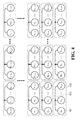
- first 302 interconnection level located in the digital domain, formed by a global network which enables distribution of numerical information corresponding to the contents of the images to all 301 modules comprising the display
- second 403 interconnection level located in the analogue domain, locally associating sub-sets G 401 modules to each other and made up of the lines necessary to perform a series connection of all LEDs and constant current sources shared by this sub-set of modules, known as 402 functional unit.
- Each circle in the two figures represents a module which has been assigned with an a r,t coefficient for the digital interconnection network and a b l,g coefficient for the local analogue network.
- the two sets of coefficients are bijectively related to each other, in a way that all coefficients in figure 3 equate to only one of the coefficients in figure 4 . This means that the physical location of each module does not have to coincide either with their position on the graph, or with their physical one. This point will be described later on.
- the 403 analogue interconnection network is limited to only one 402 functional unit of G modules, where each P/(N ⁇ G) functional unit is completely independent of the other from the analogue point of view.
- Each module has all the analogue and digital electronic system necessary to independently control the brightness of N LEDs and efficiently distribute the numerical information corresponding to images between all the modules making up the display.
- Each G module referred to as b l,g, in the figure contains at least one of the following elements for each of the three red, green and blue components:
- each of the module includes a set of no (L R +L G +L B )+ 603 analogue switches connected in parallel to each of the 501 LEDs.
- These analogue switches may be implemented by a NMOS, PMOS, PNP, NPN transistor or any valid combination of them, like for example two-way gateways (T-gates), or by any other device governed by a control inlet which allows the passage of electric current to be interrupted at will.
- each N ⁇ (L R +L G +L B ) analogue switch incorporates a 602 level adapter, in such a way that every switch is governed by the same number of digital control signals conforming the 601 digital bus; those adapters allow independent activation or deactivation of each analogue switch and therefore the individual switching on and off of each LED in the same module may be controlled from the digital domain.
- the 507 control input of the 506 current source also forms a part of the said digital bus.
- the digital bus is generated inside each module through the 702 set of N ⁇ (L R +L G +L B )+S R +S G +S B independent pulse width modulators. Values used by each modulator are calculated through the 703 block, from the values stored in the 704 double video memory. This memory is responsible, in the first place, for storing all pulse width modulation values corresponding to intensities represented in pixels of one same module at one specific point of time and, in the second place, for saving information regarding the pixel intensities of the next image to be represented. Finally, each module has a 705 digital interface which enables reception or transmission of information to the rest of the modules in the display through the mentioned digital interconnection network.
- the display can be divided into several 801 sections, each of them formed by S functional units of G modules, all these sections being identical to each other both from the physical and from the functional point of view, in a such a way that:
- a valid formula to reach this objective is to apply an identical pulse width modulation over the constant current sources of 802 modules which occupy the same position inside each of the functional units belonging to the same section.
- This pulse width modulation corresponds to that of the module with the highest consumption of all those occupying the same position inside the functional unit.
- the following examples show different configurations which may be adopted by the functional units of the G modules.
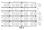
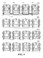
- the LEDs making up a pixel contained in the one same symbol appear in all the diagrams. They can refer indistinctly either to LEDs which are physically inside the same component or to LEDs manufactured in independent capsules.
- LEDs used in this example have the following electrical parameters as shown in Table 1: Parameter Units Green Red Blue Maximum live voltage drop Volts 4 2.5 4
- LEDs of a specific colour component present much higher brightness than really necessary either to obtain a correct white balance or to reach the minimum brightness desired for the display.
- This feature can be used to increase the number of LEDs of these colour components connected in series and belonging to the same current source in such a way that the sum of all their individual live voltages can be higher than the maximum value allowed by supply voltage of the source. This is achieved by employing the modified pulse width modulation techniques described in this patent, which ensure that, at a certain point of time, all accumulated voltage drops never exceed the maximum allowed by the supply voltage. Please note that, in contrast, the maximum light intensity possible for each LED to reach is reduced proportionally to the number of additional LEDs.
- the advantage of increasing the number of LEDs connected in the same series circuit of a specific colour component is that the number of current sources needed by the system is reduced, thus offering a much wider range of possible configurations when the number of LEDs connected in series in each colour component is made independent with respect to the value of the supply voltage.
- a parameter known as degree of use of each colour component is defined for a specific supply voltage such as the relationship between the maximum number of LEDs allowed by the supply voltage used and the total number of LEDs connected in series to the same current source.
- Figures 9B-9D represent the route of the current through the LEDs for each of the four current sources.
- the additional X modules do not include any constant current source in the functional unit, as the objective is to increase only the number of LEDs connected in series to each of the existing current sources.
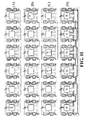
- the diagram corresponding to this setting (known as "RXGGXB”) can be seen in figure 11D .
- the degrees of use are the same as those in the original 32V setting.
- the analogue interconnection network is, in this case, totally different due to the presence of two new X modules.
- Figures 11A-11C also show the route followed by current through the LEDs for each of the four current sources.
- This additional LED is also individually addressable, which enables the implementation of pixels based on 4 LEDs.
- This modification consists of replacing the two modules marked with an "X" in figure 12 , which are not using any current source, by another two that do, so that the currents necessary to supply the additional green LEDs can be generated, resulting in the "RGGGGB" setting.
- Figures 12A-12C represent the route followed by the current through the LEDs for each of the six current sources.
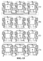
- Figures 13B-13D represent the route followed by the current through the LEDs for each of the four current sources. In this case, the degrees of use values are those shown in table 3. Parameter Units Green Red Blue Degree of use % 100 60 100
- FIG. 15A shows the preferential setting of figure 3 , whose digital interconnection network is formed by a cascade connection (or daisy chain) of 1501 C i modules, where i varies between 0 and R T-1, which works in a similar way to how a shift register would.
- These modules are interconnected through a diversity of 1502 point-to-point communication channels equivalent to the 302 digital interconnection network. Data input is carried out via the 1503 first channel. It is not relevant whether these communication channels are synchronous or asynchronous.
- each coefficient in figure 3 is equivalent to one and only one of the coefficients in figure 15A .
- the physical positions of each module do not need to be spatially coincident in both network nor with the position they occupy on the chart.
- the particular physical route of the series circuit of all modules throughout the length and breadth of the display is not relevant from the perspective of the description of this invention.
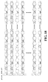
- FIG 18 shows how one of the comments from the description of the preferred setting of the invention can be applied for the data input and output to coincide in the same location while preserving the advantages of previous examples.
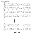
- Figure 19 shows a variation of this concept, whereby distribution of signals corresponding to horizontal group has been simplified to the detriment of vertical connection by separating the horizontal even rows from the odd; this way, the signal goes down the first and up the second.
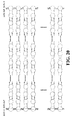
- Figure 20 contains one of the previous examples, chosen to illustrate this idea, but the same approach can be accomplished with any other configuration described in this patent.
- the process consists of placing two or more completely finished panels next to each other, either in a mirror distribution or not.
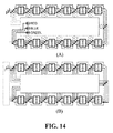
- modules belonging to each horizontal group have been arranged all along a line.
- other arrangements may be used which, although physically different, are equivalent from an electrical point of view.
- the interconnection lines comprising both may be laid out in such a way that they run in parallel along the same physical route.
- Figures 21A-21D show the different useful alternatives in this respect.
- the advantages obtained with these additional configurations are, firstly, the optimization of energy performance through the spatial and more compact distribution of pixels belonging to the same current source.
- this display shall be necessarily made up by a diversity of G-multiple modules (number of modules in each functional unit).
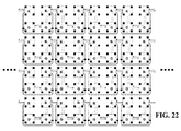
- figure 22 shows the physical implementation of a display whose functional units use an "RGGB" configuration with a compact arrangement. Please note how the analogue interconnection network has been represented by a thick line and the digital one by arrows.
- Figure 23A shows how a the vertical, cascade and adjacent connection can be made between of many 2301 individual displays such as the ones described in this paragraph through their upper and lower external connections by forming a vertical column of 2302 displays until the intended vertical dimension is reached. A number of these display columns are then placed in a horizontal and adjacent configuration reaching in order to achieve the desired horizontal dimension as shown figure 2303.
- the resulting 2305 display is completed in figure 23B with the external connection of a 2304 external modular wiring allowing distribution of video information and supplying all columns of individual displays from the exterior.
- figure 23C how this connection can be made from the upper and/or the lower side, as well as from the left and/or right side of the whole display set, thus allowing the final dimensions of the display to be further increased.
- each module there is a first group of pulse width modulators.
- the supply voltage value is not high enough to simultaneously supply all n LEDs belonging to the same series circuit through the corresponding constant current source, it is necessary to use a set of modified pulse width modulations from the first group of the said pulse width modulations as described in figure 24 .
- the working cycle value of the pulse width modulation applied to each of the LEDs is the same and equivalent to 3/12, that is to say, 0.25.
- Another overlapping pulse with modulation is applied over each original pulse width modulation.
- the frequency of the overlapping pulse width modulation is a whole, non-zero number which is E times greater than the original pulse width modulation value, while the working cycle of all overlapping pulse width modulations remains constant and with a value equal to M/n.
- Each overlapping pulse width modulation is applied with a constant phase difference equal to the T period of the overlapping pulse width modulation divided by the number of n LEDs connected in each series circuit.
- This value is represented in figures 24C and 24E by the vertical dashed line.
- table 4 confirms how the system performance quickly approaches the optimal value at the same time as the E frequency value is increased. The performance value obtained is always higher for longer working cycles.
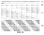
- Figure 25A and 25B show the differences between a conventional and a non-linear pulse width modulation.
- the different values which can be generated in a conventional pulse width modulation are evenly spaced and have been represented in figure 25A by vertical dotted lines.
- the number of transitions in each complete T-period of the modulation would be 65,536.
- due to the logarithmic response of human vision only a small number of these values can really be distinguished.
- a clock with a frequency which varies throughout each period of the pulse width modulation (from an initial minimum value to the maximum value, passing through the complete subset of values) has been used.
- the duration of each clock cycle applied to this modulation is directly proportional to each of the values obtained with the gamma correction formula.
- Figure 25A shows how the number of transitions is much higher than in figure 25B .
- Consumption is proportional to the number of transitions, which means that consumption obtained with this new modulation is also reduced to the same extent. For instance, in the case of a non-linear pulse width modulation equivalent to 16 bits, the number of transitions and consumptions would be reduced by a factor of 256. Please note that in this case only 8 bits would be needed to encode the whole set of representable intensities.
- each T-period of the pulse width modulation is divided into a total of 8 identical and consecutive non-linear modulations.
- a second set of overlapping pulse width modulations such as the ones described in this patent may be applied over each of the previous non-linear modulations.
- Figure 25D shows the whole set of valid and representable values.
- non-linear modulations must be able to represent the set of intensities resulting from the application of gamma correction over 2,048 initial values, i.e. a subset of 64 values noticeable to the human eye. Therefore, it is necessary to divide each period of the resulting pulse width modulation into a total of 32 consecutive and non-linear pulse width modulations, each of them able to represent 64 values in a non-linear way.
- the multiple of E-value of the overlapping pulse width modulation frequency can be further increased by reducing the number of non-linear values with respect to the linear ones, by worsening the consumption improvement factor and by increasing the number of bits necessary to implement the resulting pulse width modulation.
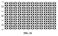
- the dashed line shows the groups of two subsets of four modules whose current consumption is balanced by the firmware governing the display. Under these conditions, the current circulating through the 32V conductor is minimal, while the section of the main earth and 64V conductors is maintained with respect to the original 32V "RGGB" configuration.
- the communications network can not only link each module to the previous one, but also includes an additional, auxiliary connection linking each module to the module before the immediately previous one. Additionally, it incorporates a system to detect the parity of data received by both channels, so that a digital logic makes it possible to automatically switch to an auxiliary channel when parity of the main channel does not coincide with that expected.
- Figure 29 shows how modules are interconnected. This action effectively disconnects the previous module from the system when there is an intermittent or temporary failure in the same. To prevent alteration of the distribution order of the data between all modules it is necessary to incorporate an additional digital logic to this auxiliary channel to compensate the fact that the system is now one module short.
Landscapes
- Engineering & Computer Science (AREA)
- Physics & Mathematics (AREA)
- Computer Hardware Design (AREA)
- General Physics & Mathematics (AREA)
- Theoretical Computer Science (AREA)
- Control Of Indicators Other Than Cathode Ray Tubes (AREA)
- Control Of El Displays (AREA)
Applications Claiming Priority (2)
| Application Number | Priority Date | Filing Date | Title |
|---|---|---|---|
| ES201130103A ES2386657B1 (es) | 2011-01-27 | 2011-01-27 | Pantalla de video de led's. |
| PCT/ES2011/070855 WO2012101294A1 (es) | 2011-01-27 | 2011-12-13 | Pantalla de video de led's |
Publications (2)
| Publication Number | Publication Date |
|---|---|
| EP2713357A1 true EP2713357A1 (de) | 2014-04-02 |
| EP2713357A4 EP2713357A4 (de) | 2017-01-11 |
Family
ID=46580237
Family Applications (1)
| Application Number | Title | Priority Date | Filing Date |
|---|---|---|---|
| EP11856909.4A Withdrawn EP2713357A4 (de) | 2011-01-27 | 2011-12-13 | Led-videobildschirm |
Country Status (3)
| Country | Link |
|---|---|
| EP (1) | EP2713357A4 (de) |
| ES (1) | ES2386657B1 (de) |
| WO (1) | WO2012101294A1 (de) |
Cited By (2)
| Publication number | Priority date | Publication date | Assignee | Title |
|---|---|---|---|---|
| EP3249639A1 (de) * | 2016-05-26 | 2017-11-29 | Nederlandse Organisatie voor toegepast- natuurwetenschappelijk onderzoek TNO | Anpassbare matrixanzeigenvorrichtung |
| KR20220155181A (ko) * | 2020-03-17 | 2022-11-22 | 보에 테크놀로지 그룹 컴퍼니 리미티드 | 발광 기판 및 그 구동 방법, 및 디스플레이 장치 |
Families Citing this family (4)
| Publication number | Priority date | Publication date | Assignee | Title |
|---|---|---|---|---|
| KR101596580B1 (ko) * | 2014-06-09 | 2016-02-23 | 삼성디스플레이 주식회사 | 스트레처블 디스플레이 및 그의 제조방법 |
| CN114373397B (zh) * | 2020-10-15 | 2023-07-18 | 合肥鑫晟光电科技有限公司 | 发光基板、发光母板、获得发光基板的方法及显示装置 |
| CN116110295B (zh) * | 2023-01-03 | 2024-07-09 | 业成光电(深圳)有限公司 | 微型显示器架构 |
| CN117995080B (zh) * | 2024-04-03 | 2024-06-25 | 山东中联晶智信息科技有限公司 | 用于led显示屏的故障数据监管方法及系统 |
Family Cites Families (10)
| Publication number | Priority date | Publication date | Assignee | Title |
|---|---|---|---|---|
| US4743897A (en) | 1985-10-09 | 1988-05-10 | Mitel Corp. | LED driver circuit |
| GB2332582A (en) * | 1997-12-18 | 1999-06-23 | Murray Shelley Richard | Large screen television display system |
| JPH11288252A (ja) * | 1998-04-01 | 1999-10-19 | Daichu Denshi:Kk | 点灯装置およびこれを用いた拡張型表示装置 |
| US7202613B2 (en) * | 2001-05-30 | 2007-04-10 | Color Kinetics Incorporated | Controlled lighting methods and apparatus |
| JP4177022B2 (ja) * | 2002-05-07 | 2008-11-05 | ローム株式会社 | 発光素子駆動装置、及び発光素子を備えた電子機器 |
| EP1513059A1 (de) * | 2003-09-08 | 2005-03-09 | Barco N.V. | Pixeleinheit für Grossoberflächeanzeigevorrichtung |
| GB0406107D0 (en) * | 2004-03-17 | 2004-04-21 | Koninkl Philips Electronics Nv | Electroluminescent display devices |
| US8344410B2 (en) * | 2004-10-14 | 2013-01-01 | Daktronics, Inc. | Flexible pixel element and signal distribution means |
| EP1898676A1 (de) * | 2006-09-06 | 2008-03-12 | THOMSON Licensing | Anzeigevorrichtung |
| ES2338962B1 (es) * | 2008-01-11 | 2011-04-04 | Senia Technologies S.L. | Configuracion de reguladores de corriente para pantallas de video flexibles a base de led's. |
-
2011
- 2011-01-27 ES ES201130103A patent/ES2386657B1/es not_active Expired - Fee Related
- 2011-12-13 WO PCT/ES2011/070855 patent/WO2012101294A1/es not_active Ceased
- 2011-12-13 EP EP11856909.4A patent/EP2713357A4/de not_active Withdrawn
Cited By (7)
| Publication number | Priority date | Publication date | Assignee | Title |
|---|---|---|---|---|
| EP3249639A1 (de) * | 2016-05-26 | 2017-11-29 | Nederlandse Organisatie voor toegepast- natuurwetenschappelijk onderzoek TNO | Anpassbare matrixanzeigenvorrichtung |
| WO2017204641A1 (en) * | 2016-05-26 | 2017-11-30 | Nederlandse Organisatie Voor Toegepast-Natuurwetenschappelijk Onderzoek Tno | Conformable matrix display device |
| US10636351B2 (en) | 2016-05-26 | 2020-04-28 | Nederlandse Organisatie Voor Toegepast-Natuurwetenschappelijk Onderzoek Tno | Conformable matrix display device |
| KR20220155181A (ko) * | 2020-03-17 | 2022-11-22 | 보에 테크놀로지 그룹 컴퍼니 리미티드 | 발광 기판 및 그 구동 방법, 및 디스플레이 장치 |
| EP4123631A4 (de) * | 2020-03-17 | 2023-02-01 | BOE Technology Group Co., Ltd. | Lichtemittierendes substrat und ansteuerverfahren dafür, und anzeigevorrichtung |
| US11651743B2 (en) | 2020-03-17 | 2023-05-16 | Boe Technology Group Co., Ltd. | Light emitting substrate, method of driving light emitting substrate, and display device |
| US11881184B2 (en) | 2020-03-17 | 2024-01-23 | Boe Technology Group Co., Ltd. | Light emitting substrate, method of driving light emitting substrate, and display device |
Also Published As
| Publication number | Publication date |
|---|---|
| WO2012101294A1 (es) | 2012-08-02 |
| ES2386657B1 (es) | 2013-07-05 |
| ES2386657A1 (es) | 2012-08-24 |
| EP2713357A4 (de) | 2017-01-11 |
Similar Documents
| Publication | Publication Date | Title |
|---|---|---|
| EP2713357A1 (de) | Led-videobildschirm | |
| US9723244B2 (en) | Low cost LED driver with improved serial bus | |
| US8493004B2 (en) | Ilumination device comprising multiple LEDs | |
| JP5229718B2 (ja) | バックライトドライバ及びこれを含む液晶表示装置 | |
| US20120327128A1 (en) | Led display systems | |
| CN103365463B (zh) | 控制触屏的方法、控制器及显示系统 | |
| US20220028328A1 (en) | LED Driving Device and LED Driving Method | |
| US9622307B2 (en) | Apparatus and technique for modular electronic display control | |
| JP7443531B2 (ja) | ディスプレイ装置のための画像要素、およびディスプレイ装置 | |
| KR20020059598A (ko) | 디스플레이장치, 디스플레이 구동회로 또는 디스플레이구동방법 | |
| KR102757305B1 (ko) | 표시 장치 | |
| TW202036512A (zh) | 顯示系統及其共用驅動電路 | |
| KR102881832B1 (ko) | 엘이디 구동회로 및 이의 구동방법 | |
| US9093022B2 (en) | Power supply device, organic light emitting display device having the same, and method of supplying power | |
| KR20120114023A (ko) | 백라이트 유닛 및 이를 포함하는 표시 장치 | |
| KR102786533B1 (ko) | 게이트 드라이버와 이를 포함한 전계 발광 표시장치 | |
| US20110050757A1 (en) | Configuration of current regulators for led-based flexible video screens | |
| Hasan et al. | A RGB-driver for LED display panels | |
| KR20090009395A (ko) | 구동 장치 및 이를 포함하는 표시 장치 | |
| KR20250016566A (ko) | Dc-dc 컨버터 및 이를 포함하는 표시 장치 | |
| KR20170080430A (ko) | 멀티비전 시스템 및 그 구동 방법 | |
| CN118155553B (zh) | 一种led阵列显示单元、显示屏以及显示系统 | |
| KR102727531B1 (ko) | 데이터 구동 회로 및 디스플레이 장치 | |
| KR20250124500A (ko) | 전원 공급부 및 이를 포함하는 표시 장치 | |
| KR102453564B1 (ko) | 백라이트유닛 및 이를 포함하는 표시장치 |
Legal Events
| Date | Code | Title | Description |
|---|---|---|---|
| PUAJ | Public notification under rule 129 epc |
Free format text: ORIGINAL CODE: 0009425 |
|
| PUAI | Public reference made under article 153(3) epc to a published international application that has entered the european phase |
Free format text: ORIGINAL CODE: 0009012 |
|
| 17P | Request for examination filed |
Effective date: 20140110 |
|
| AK | Designated contracting states |
Kind code of ref document: A1 Designated state(s): AL AT BE BG CH CY CZ DE DK EE ES FI FR GB GR HR HU IE IS IT LI LT LU LV MC MK MT NL NO PL PT RO RS SE SI SK SM TR |
|
| RIN1 | Information on inventor provided before grant (corrected) |
Inventor name: BOSCH ESTEVE, JOSE VICENTE |
|
| DAX | Request for extension of the european patent (deleted) | ||
| RIC1 | Information provided on ipc code assigned before grant |
Ipc: G09G 5/00 20060101ALI20160818BHEP Ipc: G09G 3/32 20060101AFI20160818BHEP Ipc: H05B 33/08 20060101ALI20160818BHEP |
|
| RA4 | Supplementary search report drawn up and despatched (corrected) |
Effective date: 20161208 |
|
| RIC1 | Information provided on ipc code assigned before grant |
Ipc: G09G 3/32 20160101AFI20161202BHEP Ipc: G09G 5/00 20060101ALI20161202BHEP Ipc: H05B 33/08 20060101ALI20161202BHEP |
|
| STAA | Information on the status of an ep patent application or granted ep patent |
Free format text: STATUS: THE APPLICATION IS DEEMED TO BE WITHDRAWN |
|
| 18D | Application deemed to be withdrawn |
Effective date: 20170701 |