EP2715384B1 - Procédé de fonctionnement d'un ensemble capteur à effet hall et ensemble capteur à effet hall - Google Patents
Procédé de fonctionnement d'un ensemble capteur à effet hall et ensemble capteur à effet hall Download PDFInfo
- Publication number
- EP2715384B1 EP2715384B1 EP12728424.8A EP12728424A EP2715384B1 EP 2715384 B1 EP2715384 B1 EP 2715384B1 EP 12728424 A EP12728424 A EP 12728424A EP 2715384 B1 EP2715384 B1 EP 2715384B1
- Authority
- EP
- European Patent Office
- Prior art keywords
- value
- hall sensor
- signal
- input signal
- values
- Prior art date
- Legal status (The legal status is an assumption and is not a legal conclusion. Google has not performed a legal analysis and makes no representation as to the accuracy of the status listed.)
- Active
Links
Images



Classifications
-
- G—PHYSICS
- G01—MEASURING; TESTING
- G01R—MEASURING ELECTRIC VARIABLES; MEASURING MAGNETIC VARIABLES
- G01R33/00—Arrangements or instruments for measuring magnetic variables
- G01R33/02—Measuring direction or magnitude of magnetic fields or magnetic flux
- G01R33/06—Measuring direction or magnitude of magnetic fields or magnetic flux using galvano-magnetic devices
- G01R33/07—Hall effect devices
- G01R33/072—Constructional adaptation of the sensor to specific applications
-
- G—PHYSICS
- G01—MEASURING; TESTING
- G01R—MEASURING ELECTRIC VARIABLES; MEASURING MAGNETIC VARIABLES
- G01R33/00—Arrangements or instruments for measuring magnetic variables
- G01R33/0023—Electronic aspects, e.g. circuits for stimulation, evaluation, control; Treating the measured signals; calibration
- G01R33/0029—Treating the measured signals, e.g. removing offset or noise
-
- G—PHYSICS
- G01—MEASURING; TESTING
- G01R—MEASURING ELECTRIC VARIABLES; MEASURING MAGNETIC VARIABLES
- G01R33/00—Arrangements or instruments for measuring magnetic variables
- G01R33/0023—Electronic aspects, e.g. circuits for stimulation, evaluation, control; Treating the measured signals; calibration
- G01R33/0035—Calibration of single magnetic sensors, e.g. integrated calibration
-
- G—PHYSICS
- G01—MEASURING; TESTING
- G01R—MEASURING ELECTRIC VARIABLES; MEASURING MAGNETIC VARIABLES
- G01R33/00—Arrangements or instruments for measuring magnetic variables
- G01R33/02—Measuring direction or magnitude of magnetic fields or magnetic flux
- G01R33/06—Measuring direction or magnitude of magnetic fields or magnetic flux using galvano-magnetic devices
- G01R33/07—Hall effect devices
-
- G—PHYSICS
- G01—MEASURING; TESTING
- G01R—MEASURING ELECTRIC VARIABLES; MEASURING MAGNETIC VARIABLES
- G01R33/00—Arrangements or instruments for measuring magnetic variables
- G01R33/02—Measuring direction or magnitude of magnetic fields or magnetic flux
- G01R33/06—Measuring direction or magnitude of magnetic fields or magnetic flux using galvano-magnetic devices
- G01R33/07—Hall effect devices
- G01R33/072—Constructional adaptation of the sensor to specific applications
- G01R33/075—Hall devices configured for spinning current measurements
Definitions
- the present invention relates to a method for operating a Hall sensor arrangement and a Hall sensor arrangement.
- Hall sensor arrangements are used to determine a magnetic field.
- Hall sensors usually show an offset voltage, that is a non-zero output voltage between two contacts of the Hall sensor, provided that a current flows between two other contacts of the Hall sensor, even if the Hall sensor is not in a magnetic field.
- the sensor element comprises a measuring element with four contact terminals, a switching device and a control device.
- a tax will be between a first and a second contact terminal in a first measurement phase with a first polarity and in a second measurement phase applied with a polarity opposite to the first polarity.
- the object of the present invention is to provide a method for operating a Hall sensor arrangement and a Hall sensor arrangement with which a residual offset value can be determined during operation.
- a method for operating a Hall sensor arrangement comprises setting at least two values, which are different in magnitude, of an input signal of a Hall sensor of the Hall sensor arrangement. Furthermore, the associated values of an output signal of the Hall sensor are determined. In addition, a residual offset value of the output signal is determined as a function of the values of the output signal which were determined at the at least two values of the input signal.
- the offset component of the output signal and the magnetic field-dependent useful component of the output signal depend in different ways on the height of the input signal of the Hall sensor. Therefore, advantageously by applying the Hall sensor with two different in height values of the input signal, the residual offset value of the output signal can be determined.
- a calibration of the Hall sensor arrangement by means of determining the residual offset value in Operation possible.
- the calibration can also be carried out with an applied external magnetic field of unknown magnetic field strength.
- the output signal is provided only after complete cycling through the phases of a cycle of the current spinning technique.
- the value of the input signal is constant during the phases of the cycle of the current spinning technique.
- the values of the output signal associated with the at least two values of the input signal are each provided by means of a separate cycle of the current spinning technique.
- the at least two values of the output signal are thus determined at the at least two values of the input signal by means of at least two cycles of the current spinning technique.
- the current spinning technique can be referred to as current-rotation technology, current-rotation method or method of rotating operating currents.
- the offset in the values of the output signal is already reduced by the current spinning technique before the residual offset value is determined by the evaluation of the at least two values of the output signal and a magnetic field signal is generated by the Hall sensor arrangement which has no offset influence or an offset influence has significantly reduced offset influence. Consequently, advantageously, the magnetic field signal indicates the magnetic field strength with high accuracy.
- the input signal can be realized as current or voltage.
- the residual offset value is calculated in dependence on the at least two values of the input signal and the values of the output signal determined at the at least two values of the input signal.
- the residual offset value is calculated as a function of the values of the output signal determined at the at least two values of the input signal and a scaling factor between two values of the set of the at least two values of the input signal.
- the scaling factor and a value from the set of at least two values of the input signal may be used in determining the remainder offset value.
- the scaling factor is used in determining the residual offset value.
- the calculation does not include any value of the input signal.
- the at least two values of the input signal are predetermined values.
- the calculation of the residual offset value in the Hall sensor arrangement can advantageously be simplified in such a way that the values of the input signal are combined with other parameters in equations and are no longer explicitly stated.
- the residual offset value may be a residual offset voltage or an offset factor.
- a calibration phase is connected between a first and a second operating phase.
- the residual offset value is determined.
- the value of the magnetic field is determined as a function of the residual offset value.
- the Hall sensor arrangement is operated in a first calibration phase, then in the first operating phase, then again in a second calibration phase and then again in the second operating phase. Since the Hall sensor arrangement can advantageously be calibrated during operation, calibration and operating phases can alternate several times. Thus, the influence of changes in the offset value, which are produced by aging, temperature changes or mechanical stress, for example in soldering processes, can be reduced.
- the calibration phase is triggered when a trigger signal is supplied to the Hall sensor assembly.
- a clock signal is generated which starts a calibration phase at predetermined time intervals.
- the clock signal has a constant frequency.
- the calibration phase is triggered when a temperature change of the Hall sensor arrangement is greater than a predetermined limit value.
- the Hall sensor arrangement has a temperature sensor which provides a temperature signal with which the temperature change is determined.
- the Hall sensor arrangement can be integrated in a system.
- a system may be, for example, a motor vehicle, a machine tool, an ammeter, a compass or a robot.
- the calibration phase is triggered while the system is in an idle state.
- the disturbances are kept low in a resting state of the system, so that a particularly high accuracy in the determination of the residual offset value is achieved.
- the residual offset value is a residual offset voltage.
- VOFF is the value of the residual offset voltage
- k is the value of an offset factor
- I is the value of the input signal
- n is the value of an exponent.
- the residual offset value is an offset factor.
- V is the value of the output signal
- B is the value of the magnetic field
- S is the value of a sensitivity
- I is the value of the input signal
- VOFF is the value of the residual offset voltage.
- the value of the sensitivity is predetermined.
- a coil is arranged in such a way to the Hall sensor, that the magnetic field of the coil influences the magnetic field detected by the Hall sensor, and the value of the sensitivity is determined at the at least two values of the input signal by means of the coil.
- the Hall sensor arrangement is suitable or designed for carrying out the method for operating the Hall sensor arrangement.
- a Hall sensor arrangement comprises a Hall sensor, a signal source and a determination unit.
- the signal source is coupled to an input of the Hall sensor.
- the determination unit is coupled to an output of the Hall sensor.
- the signal source is set up to provide at least two absolute values of an input signal of the Hall sensor.
- the determination unit is set up to determine a residual offset value of an output signal of the Hall sensor as a function of the values of the output signal which are determined at the at least two values of the input signal.
- the residual offset value can be determined by means of two different values of the input signal.
- the Hall sensor comprises a Hall element and an input circuit having an input of the Hall sensor with the Hall element connects. Furthermore, the Hall sensor comprises an output circuit and an evaluation circuit which connect the Hall element to an output of the Hall sensor. The output circuit and the evaluation circuit are connected in series with each other. An output signal provided by the evaluation circuit is provided only after completely passing through the phases of a cycle of the current spinning technique. The input circuit, the output circuit and the evaluation circuit are used to carry out the current spinning technique.
- At least one value of the input signal is at least 1.5 times the smallest value of the input signal. There is thus at least a difference of 50% between two values of the input signal, so that the values of the input signal and thus the values of the output signal differ significantly. This facilitates numerical stable calculation of the residual offset value.
- the Hall sensor arrangement may comprise a semiconductor body.
- the semiconductor body may comprise a silicon substrate.
- the Hall sensor, the signal source and the detection unit are arranged on a first main surface of the semiconductor body.
- the Hall sensor assembly includes a coil.
- the coil may be arranged on the first main surface of the semiconductor body.
- the coil can be a Hall sensor be arranged so that the coil generates a magnetic field which is detected by the Hall sensor.
- the Hall sensor detects the sum of the external magnetic field and the magnetic field generated by the coil.
- FIG. 1A shows an exemplary embodiment of a Hall sensor assembly.
- the Hall sensor arrangement 10 comprises a Hall sensor 11, a signal source 12 and a determination unit 13.
- the signal source 12 is connected at an output to an input of the Hall sensor 11.
- An output of the Hall sensor 11 is coupled to a signal input of the determination unit 13.
- a control output of the determination unit 13 in turn is connected to an input of the signal source 12.
- the Hall sensor 11 comprises a Hall element 14, an input circuit 15 and an output circuit 16.
- the input circuit 15 connects the input of the Hall sensor 11 with the Hall element 14.
- the Hall element 14 is connected via the output circuit 16 to the output of the Hall sensor 11.
- An evaluation circuit 17 is arranged between the output of the output circuit 16 and the output of the Hall sensor 11. Between the output of the output circuit 16 and the evaluation circuit 17, an amplifier 18 is arranged.
- the determination unit 13 has a control circuit 19, a memory 20 and a calculation unit 21.
- the memory 20 is connected to the signal input of the determination unit 13. Furthermore, the memory 20 is coupled to the calculation unit 21 and the control circuit 19. Likewise, the calculation unit 21 is connected to the control circuit 19.
- the control circuit 19 is connected to the control output of the determination unit 13.
- the determination unit 13 has a further memory 22 and a subtracter 23. An input of the subtractor 23 is connected to the signal input of the determination unit 13. Another input of the subtracter 23 is via the further memory 22 is coupled to an output of the calculation unit 21.
- the determination unit 13 comprises a comparator 24, which is connected on the input side to the memory 20 and the control circuit 19.
- the determination unit 13 has a trigger input 25.
- the determination unit 13 is implemented as a digital signal processor. Alternatively, the determination unit 13 is implemented as a microcontroller or microprocessor.
- the signal source 12 outputs an input signal I to the Hall sensor 11.
- the input signal I is realized as a current.
- the signal source 12 is designed as a bias circuit.
- the Hall sensor 11 provides an output signal V at its output.
- the output signal V is in the form of a voltage.
- the input circuit 15, the Hall element 14 and the output circuit 16 convert the input signal I into a sensor signal VS.
- the input circuit 15, the Hall element 14 and the output circuit 16 together form a chopped sensor element.
- the sensor signal VS is converted by the amplifier 18 into an amplified sensor signal AV.
- the evaluation circuit 17 generates from the amplified sensor signal AV, the output signal V of the Hall sensor 11.
- the evaluation circuit 17 is implemented as a de-chop circuit.
- the evaluation circuit 17 may include a switch, an inverter, a comparator or an analog-to-digital converter.
- the output signal V is fed to the signal input of the determination unit 13.
- the output signal V is supplied to the memory 20 and the subtracter 23.
- the subtracter 23 outputs a magnetic field signal SB on the output side.
- the subtractor 23 is implemented as a digital subtractor.
- a trigger signal STR at the trigger input 25 triggers a calibration according to one of the methods described below.
- the input circuit 15 and the output circuit 16 have switches. Thus, according to the current spinning technique, the terminals of the Hall element 14 are periodically switched.
- the sensor signal VS and the amplified sensor signal AV thus depend on the position of the switches in the input and output circuits 15, 16.
- the evaluation circuit 17 is designed to generate the output signal V from the sensor signal VS or the amplified sensor signal AV.
- the output signal V is thus provided after carrying out the current spinning technique.
- the output signal V is generated by the evaluation circuit 17 from the values of the sensor signal VS or the amplified sensor signal AV generated during a period of one cycle of the current spinning technique.
- the output signal V thus has only a small offset signal component, which is also referred to as the residual offset signal component.
- the determination unit 13 is implemented such that it determines a residual offset value in the form of a residual offset voltage VOFF and stores it in the further memory 22.
- the subtracter 23 thus subtracts the residual offset voltage VOFF from the output signal V, so that the magnetic field signal SB has a significantly reduced residual offset component.
- the magnetic field signal SB emitted by the subtracter 23 is thus approximately offset-free.
- the magnetic field signal SB is directly proportional to the magnetic field B.
- VOFF is the value of the residual offset voltage
- k is the value of an offset factor
- I is the value of the input signal
- n is the value of an exponent.
- the offset factor k is a unit-based number.
- the offset factor k has the unit volt / ampere n .
- the Hall sensor 11 has an analog-to-digital converter which is arranged between the evaluation circuit 17 and the output of the Hall sensor 11.
- the output signal V is thus present as a digital signal.
- the output signal V is designed as a current.
- the input signal I is realized as a voltage.
- the output signal V may be a voltage or a current.
- the Hall sensor arrangement 10 comprises further Hall elements.
- the further Hall elements can form a Hall sensor array together with the Hall element 14.
- the different Hall elements can be connected in parallel and / or in series with one another.
- the determination unit 13 may be designed to determine an angle information from the signal of a plurality of Hall sensors.
- the determination unit 13 can be designed to determine the angle information from the signal of a plurality of Hall sensors in accordance with the method of the coordinate rotation digital computer, abbreviated CORDIC method.
- the determination unit 13 can use alternative algorithms, such as the calculation by means of a table, English lookup table, for determining the angle information from the signal of several Hall sensors.
- FIG. 1B shows an exemplary measurement at a Hall sensor 11.
- the output signal V, the residual offset voltage VOFF and the magnetic field signal SB are indicated.
- Figure 1C shows the in FIG. 1B specified values of the residual offset voltage VOFF in an enlarged view.
- the residual offset voltage VOFF is plotted against the input signal I.
- the solid line was calculated from the measured values according to the least squares principle.
- the residual offset value VOFF is proportional to I 3.2238 .
- the non-linear dependence of the residual offset voltage VOFF on the input signal I is used to extract the residual offset voltage VOFF from at least two measurements taken at two different values of the input signal I.
- V ⁇ 2 B ⁇ S I ⁇ 2 ⁇ I ⁇ 2 + VOFF ⁇ 2 .
- VOFF ⁇ 2 k ⁇ I ⁇ 2 n .
- V1 and V2 are a first and a second value of the output signal
- B the value of a magnetic field
- S (I1) and S (I2) the first and the second value of a sensitivity
- I1 and 12 of the first and the second value of the input signal and VOFF1 and VOFF2 are the first and the second value of the residual offset voltage, respectively.
- the absolute value of the first value I1 of the input signal I and the absolute value of the second value 12 of the input signal I are different.
- the absolute value of the first value I1 of the input signal I is smaller than the absolute value of the second value 12 of the input signal I.
- the predetermined value Iv of the input signal I may be equal to the first value I1 or the second value 12 or a value of the input signal I lying between the first value I1 and the second value 12.
- vv B ⁇ S iv ⁇ iv + VOFFv .
- VOFFv k ⁇ iv n .
- the predetermined value Iv of the input signal I may be outside the range limited by the first value I1 and the second value 12.
- the measurement duration can be the period of a cycle of the current spinning technique.
- the ratio of the measurement duration at the first value 12 to the measurement duration at the second value I1 can be greater than the ratio I1 / I2, provided I1> I2.
- the ratio of the measurement duration at the first value 12 to the measurement duration at the second value I1 can be smaller than the ratio I1 / I2, provided I1 ⁇ I2. Thus, the influence of the noise is reduced.
- the current dependence of the sensitivity S is neglected. Furthermore, a given value is used for the exponent n.
- VOFF ⁇ 1 k ⁇ I ⁇ 1 n .
- VOFF ⁇ 2 k ⁇ I ⁇ 2 n .
- VOFFv k ⁇ iv n .
- At least one of the values I1, 12, Iv of the input signal I, the offset voltage VOFF and / or the offset factor k are stored in the further memory 22.
- not only the offset factor k, but also the value of the exponent n are determined.
- the first and second values V1, V2 of the output signal V at the first and second values I1, 12 of the input signal I and additionally a third value V3 of the output signal V at a third value 13 of the input signal I are measured.
- the first, the second and the third value I1, 12, 13 of the input signal I have different amounts.
- the determination of the quantities k, n and VOFF takes place by means of an iterative calculation method.
- VOFF ⁇ 3 k ⁇ I ⁇ 3 n . I ⁇ 1 ⁇ I ⁇ 2 ⁇ I ⁇ 3
- the control circuit 19 sets the signal source 12 by means of the control signal SI such that the first value I1 of the input signal I is provided to the Hall sensor 11. The first value V1 of the output signal V of the Hall sensor 11 is then stored in the determination unit 13 in the memory 20. Furthermore, the control circuit 19 provides the second value 12 of the input signal I by means of the control signal SI, and the second value V2 of the output signal V is stored in the determination unit 13 in the memory 20. Furthermore, the signal source 12 is adjusted by control circuit 19 by means of the control signal SI such that the third value 13 of the input signal I is output to the Hall sensor 11, which in turn provides the third value V3 of the output signal V. The third value V3 of the output signal V is stored in the memory 20.
- the determination unit 13 calculates the value of the exponent n and the value of the offset factor k. Furthermore, the determination unit 13 calculates the value of the residual offset voltage VOFF, for example, at the first, second or third value I1, 12, 13 of the input signal I or a further predetermined value Iv of the input signal I and from this the value of the magnetic field signal SB or the value of the product the value of the magnetic field B and the value of the sensitivity S.
- the first and second embodiments of the method are based on the assumption that the value of the magnetic field B changes only very slightly during the duration of the calibration phase.
- the residual offset voltage VOFF is further reduced by a factor of 0.5 to 0.01 compared to the value of the residual offset voltage VOFF, which has already been reduced by application of the current spinning technique.
- the effort for carrying out the first and the second embodiment the method kept low; For example, no coil is needed.
- the shortest measuring duration is set and for the largest value of the three values I1, 12, 13 of the input signal I the shortest measuring duration.
- a measurement duration between the shortest and the longest measurement duration is set.
- the calibration is performed and then verified.
- the first value I1 of the input signal I is first generated during the calibration phase, the first value V1 of the output signal V is stored, and then the second value 12 of the input signal I is generated.
- the measurement is repeated with the first value I1 of the input signal I and the associated newly determined value V1 'of the output signal V is compared with the first value V1 of the output signal V determined during the calibration phase. The comparison is carried out by the comparator 24 in the determination unit 13. If the two values V1 and V1 'match, it can be assumed that the strength of the magnetic field B has not changed significantly during the calibration phase and the values determined for the offset factor k and the exponent n are used in the subsequent operating phase can.
- further measurements are carried out as control measurements.
- systematic errors due to unfavorable frequency components can be detected.
- At least one value of the input signal I is greater than 1 mA. In an alternative embodiment At least one value of the input signal I is greater than 2 mA.
- FIG. 1D shows an example of measurement results obtained with the first embodiment of the method.
- 19 different Hall sensors were measured.
- the value of the input signal I was 2.25 mA.
- a residual offset voltage VOFF calculated according to the first embodiment of the method a measured residual offset voltage VOFFC and a remaining residual offset voltage VOFFR are indicated.
- the values VOFFC were measured without an external applied field except for the earth magnetic field, whereby the earth magnetic field was not shielded during the measurement.
- the values VOFF of the calculated residual offset voltages were extracted from measurement data determined with an applied external magnetic field of 1.6 mT by the method given above.
- the value VOFFR is the difference between the measured values VOFFC of the residual offset voltage and the calculated values VOFF of the residual offset voltage and corresponds to the strength of the earth's magnetic field in the measuring chamber.
- FIG. 1D thus shows that an offset calibration with an applied external magnetic field, here of 1.6 mT, is possible.
- FIG. 2A shows a further exemplary embodiment of the Hall sensor assembly.
- the Hall sensor assembly 10 according to FIG. 2A is a further education of in Figure 1A shown Hall sensor arrangement.
- the Hall sensor assembly 10 includes a coil 30 which is coupled to the Hall sensor 11.
- the coil 30 is arranged on the Hall element 14.
- the coil 30 is arranged in such a way that the magnetic field generated by the coil 30 contributes to the magnetic field measured by the Hall element 14.
- the Hall sensor assembly 10 includes a power generator 31, whose output is connected to the coil 30. Another control output of the determination unit 13 is connected to the power generator 31.
- the control circuit 19 is connected on the output side to the current generator 31.
- the current generator 31 provides a coil current IC which is supplied to the coil 30.
- the magnetic field generated by the coil 30 is proportional to the value of the coil current IC.
- the determination unit 13 generates a further control signal SIC, which is supplied to the current generator 31 and controls the value of the coil current IC.
- FIG. 2B shows a further exemplary embodiment of the Hall sensor assembly, which is a development of in Figures 1A and 2A shown Hall sensor arrangements is.
- the signal source 12 comprises a current source 32 whose output is connected to the Hall sensor 11.
- the current source 32 is realized controlled.
- the signal source 12 to a digital-to-analog converter 33.
- the current source 32 forms a current output of the digital-to-analog converter 33.
- the current generator 31 is also realized as a current source.
- the power source of the power generator 31 is implemented under control.
- the current source of the current generator 31 represents a further output of the digital-to-analog converter 33.
- the digital-to-analog converter 33 is thus realized as a two-channel digital-to-analog converter.
- the evaluation circuit 17 comprises a low-pass filter. Further, the Hall sensor 11 comprises an analog-to-digital converter 34, which is arranged between the evaluation circuit 17 and the output of the Hall sensor 11. The analog-to-digital converter 34 is connected on the output side to the signal input of the determination unit 13. Furthermore, the Hall sensor arrangement 10 a reference source 35. The reference source 35 is connected to a reference input of the analog-to-digital converter 34.
- the memory 20 and the further memory 22 form in FIG. 2B a shared memory block. The memory 20 and the further memory 22 have memory cells for storing a coil factor CS, various predetermined values I1, 12, 13, Iv of the input signal I and / or different predetermined values of the coil current IC.
- the control circuit 19 has its output connected to the input circuit 15, the output circuit 16, the amplifier 18 and the analog-to-digital converter 34.
- the control circuit 19 thus controls the position of the switches of the input and output circuits 15, 16 for performing the current spinning technique.
- the amplifier 18 is adjusted.
- the amplifier 18 is realized as a chopping amplifier.
- the control circuit 19 controls the analog-to-digital converter 34. It is thereby achieved that a measured value is provided as the output signal V of the determination unit 13 only after a complete cycle has been carried out according to the spinning technique.
- the reference circuit 15 provides a reference signal VREF, which is supplied to the analog-to-digital converter 34.
- the dependence of the sensitivity S (I) on the input signal I is taken into account.
- the dependence of the sensitivity S (I) on the input signal I is determined by means of the coil 30.
- V i + IC is the value of the output signal at a positive coil current and the i-th direction
- V i -IC the value of the output signal at a negative coil current and the ith direction
- IC the value of the coil current and CS the value of the coil factor the coil 30 is.
- the determination of the sensitivity S (I) can be carried out in the presence of an external magnetic field.
- the value of the output signal V is determined to be a value 0 of the coil current IC, at a positive value and at a negative value of the coil current IC.
- the absolute values of the positive and negative values of the coil current IC are identical. Since the determination unit 13 now takes into account the current dependence of the sensitivity S (I), an accurate value of the magnetic field signal SB is determined.
- the sensitivity S (I) and the output signal V at the first and second values I1, 12 of the input signal I are determined by means of the coil 30 during the calibration phase.
- a given value for the exponent n is used.
- the first or the second value I1, 12 of the input signal is used.
- the signal source 12 outputs the first value I1 of the input signal I.
- VOFF ⁇ 2 k ⁇ I ⁇ 2 n .
- the corresponding values V1, V2, V3 of the output signal V are determined in the calibration phase at least for the first, second and third values I1, 12, 13 of the input signal I and also at the first, second and third values I1, 12, 13 of the input signal I, the three values S (I1), S (I2), S (I3) of the sensitivity S (I) are determined by means of the coil 30.
- the value of the exponent n and then the value of the offset factor k determine.
- the already stated iterative calculation method is used.
- a S I ⁇ 3 ⁇ I ⁇ 3 ⁇ V ⁇ 2 ⁇ S I ⁇ 3 ⁇ I ⁇ 3 - V ⁇ 3 ⁇ S I ⁇ 2 ⁇ I ⁇ 2 .
- b S I ⁇ 3 ⁇ I ⁇ 3 ⁇ V ⁇ 3 ⁇ S I ⁇ 1 ⁇ I ⁇ 1 - V ⁇ 1 ⁇ S I ⁇ 3 ⁇ I ⁇ 3 .
- c S I ⁇ 3 ⁇ V ⁇ 1 ⁇ S I ⁇ 2 ⁇ I ⁇ 2 - V ⁇ 2 ⁇ S I ⁇ 1 ⁇ I ⁇ 1 .
- the N values I1, 12, 13, ..., IN the N values V (I1), V (I2), V (I3), ..., V (IN) of the output signal V are determined.
- the first value VOFF1 of the residual offset voltage from the first and the second value V1, V2 of the output signal V the second value VOFF2 the residual offset voltage from the second and the third Value V2, V3 of the output signal V and the N-1te value VOFF_N-1 of the offset voltage from the N-1ten and the Nth value V of the output voltage V determined.
- the first value n1 of the exponent n is calculated.
- the extraction of the first value VOFF1 to the N-1th value VOFF_N-1 of the residual offset voltage VOFF is repeated.
- the iterative calculations continue.
- Figure 2C shows exemplary measurement results that were determined with the third embodiment of the method.
- a value n 3.0 was assumed for the exponent n.
- the value of the input signal I was 2.25 mA.
- FIG. 2D shows an example of measurement results obtained with the fourth embodiment of the method.
- the determined value of the exponent n is different in the various examples of the Hall sensor assemblies 10 and is in a range of 2.88 to 3.17.
- Figures 2C and 2D For each of the 19 examples of the Hall sensor arrangement, the associated values of the residual offset voltage VOFF calculated according to the method described above, the measured residual offset voltage VOFFC, and the remaining residual offset voltage VOFFR are indicated. As already at FIG. 1D 1, the values VOFFC were measured when only the earth's magnetic field influenced the Hall sensor 11.
- the values VOFF of the calculated residual offset voltages were extracted with the third and fourth embodiments of the method from measurement data at an external magnetic field of 1.6 mT.
- the value VOFFR is the difference between the measured values VOFFC and the calculated values VOFF and corresponds to the strength of the earth's magnetic field in the measuring chamber.
- a particularly high accuracy in the determination of the magnetic field B is achieved by means of the third and the fourth embodiment of the method.
- FIG. 3A shows a further exemplary embodiment of the Hall sensor assembly.
- the Hall sensor assembly 10 according to FIG. 3A is a further education in the Figures 1A . 2A and 2B shown embodiments.
- the determination unit 13 has a status signal output 40. At the status signal output 40, the determination unit 13 outputs a status signal STS.
- the status signal STS has a first value during the operating phase and a second value during the calibration phase of the Hall sensor arrangement 10. The status signal STS can thus be used to indicate whether the iterative calibration is complete in the calibration phase.
- the output signal V which can be tapped off at the output of the Hall sensor 11 already corresponds to the magnetic field signal SB.
- the output signal V is fed to the control circuit 19 of the determination unit 13.
- the output signal V is already free from the residual offset value VOFF as soon as the status signal STS indicates that the calibration phase has been successfully completed.
- the subtracter 23 can thus in the embodiment according to FIG. 3A omitted.
- FIG. 3B shows a further exemplary embodiment of the Hall sensor assembly, a further development of the in the Figures 1A . 2A . 2 B and 3A shown embodiments.
- the memory 20 has memory cells for storing the sensitivity S and the coil factor CS.
- the calculation unit 21 determines the value of the exponent n, the offset factor k and the value of the coil current IC.
- the coil current IC thus has no predetermined value.
- the coil current IC has a variable value.
- the coil current IC is provided by means of the digital-to-analog converter 33 and the current generator 31.
- the amplifier 18, the evaluation circuit 17 and the analog-to-digital converter 34 may together be referred to as a channel.
- the evaluation circuit 17 is used for Offsetreduzi für, which is achieved due to the current spinning technique.
- the calculation circuit 21 calculates the value of the exponent n and the value of the offset factor k to determine the value of the coil current IC.
- the output signal V obtained is free from the residual offset voltage VOFF after the calibration phase.
- the calibration phase can also be referred to as the start phase.
- the residual offset voltage VOFF is compensated by means of a magnetic field, which is generated by means of the coil 30.
- the value of the coil current IC depends on the value of the input signal I of the Hall sensor 11 and is determined by means of an iterative method during the calibration phase. While in the first four embodiments of the method the residual offset voltage VOFF is subtracted from the measured value of the output signal V, in the fifth embodiment of the method the magnetic field of the coil 30 compensates for the residual offset voltage VOFF and the output signal V is directly proportional to the magnetic field B.
- the output signal V at the first, second and third values I1, 12, 13 of the input signal I is measured.
- a quasi-permanent recalibration is performed.
- the Hall sensor 11 is calibrated and then determined in the operating phase of the output signal V exclusively at a value, that is about the first, second or third value I1, 12, 13 of the input signal I.
- a recalibration can be triggered according to one of the methods described above.
- the Hall sensor 11 is subjected to three different values I1, 12, 13 of the input signal I.
- the input signal I is realized as current flowing through the Hall element 14.
- a residual offset voltage VOFF is regulated back, in that the coil current IC flows through the coil 30.
- the output signal V increases linearly with the input signal I.
- the value of the exponent n and the value of the offset factor k can be calculated analytically by the determination unit 13.
- the method begins with a value zero of the coil current IC at a first operating point and determines the necessary values of the coil current IC for the second and third operating point such that a linear relationship between the output signal V and the input signal I is achieved.
- the input signal I assumes the first value I1, in the second operating point the input signal I the second value 12 and in the third operating point of the input signal I the third value 13.
- the value of the exponent n and the value of the offset factor k are calculated from the value of the coil current IC and serve as parameters for the calculation of the coil current IC at the first operating point in the next iteration run. Consequently, the value of the exponent n and the value of the offset factor k are determined in an iterative manner.
- VOFF k ⁇ I ⁇ 2 n .
- V ⁇ 2 ⁇ ⁇ 2 ⁇ V ⁇ 1 .
- V ⁇ 3 ⁇ ⁇ 3 ⁇ V ⁇ 1 .
- I ⁇ 2 ⁇ ⁇ 2 ⁇ I ⁇ 1 .
- I ⁇ 3 ⁇ ⁇ 3 ⁇ I ⁇ 1 .
- I ⁇ 2 ⁇ ⁇ 2 ⁇ I ⁇ 1 .
- I ⁇ 3 ⁇ ⁇ 3 ⁇ I ⁇ 1 .
- IC ⁇ 2 ⁇ ⁇ 2 ⁇ I ⁇ 1 .
- CS is the coil factor
- S the sensitivity
- V1 the value of the output signal V at the first value I1 of the input signal I
- V2 the second value of the output signal V at the second value 12 of the input signal I
- V3 the third value of the output signal V at the third value 13 of the input signal I
- IC1 is the first value of the coil current
- IC2 is the second value of the coil current
- IC3 is the third value of the coil current.
- the above loop is run through several times until a convergence criterion is met.
- FIG. 3C shows exemplary results achieved with the fifth embodiment of the method. It is the Output voltage V applied over the input signal I.
- the uppermost curve shows the output signal V without compensation, that is at a value zero of the coil current IC.
- the magnetic field signal SB is given, which corresponds to an ideal signal.
- the value of the magnetic field signal SB depends linearly on the value of the input signal I.
- the output signal V at the sixth iteration step is already very close to the ideal signal.
- the value of the magnetic field was about 50 ⁇ T. The calculations were done with test data.
- Figure 3D shows another exemplary embodiment of the Hall sensor assembly 10, which is a development of the Hall sensor arrangements shown in Figures 1A, 2A, 2B, 3A and 3B.
- the compensation unit 37 comprises a compensation current source 38.
- the compensation current source 38 is connected to the output of the output circuit 16.
- the Hall sensor 11 has a zero point detector 41.
- the zero point detector 41 is arranged between the evaluation circuit 17 and the output of the Hall sensor 11.
- the zero point detector 41 is connected on the output side to the input of the determination unit 13.
- the zero point detector 41 comprises a comparator.
- the evaluation circuit 17 is realized as a low-pass filter.
- the amplifier 18 is designed as an auto-amplifier.
- the output signal V of the Hall sensor 11 thus has the logical values zero and one.
- the magnetic field signal SB is provided by the calculation unit 21.
- a compensation current IK flows through the compensation current source 38.
- the Compensation unit 37 eliminates a part of the offset. The range for the values of the coil current IC can be made small, in that the offset is reduced by means of the compensation unit 37.
- a sixth embodiment of the method is described with the aid of in Figure 3D realized Hall sensor assembly 10 realized.
- the magnetic field B can be determined by the coil current IC flowing through the coil 30.
- the Hall sensor assembly 10 may be used as an electronic compass.
- the sixth embodiment of the method is particularly suitable for the determination of small values of the magnetic field B.
- the value of the exponent n and the value of the offset factor k are extracted as indicated above.
- a first operating point is set.
- the third value 13 of the input signal is output from the signal source 12 and fed to the Hall sensor 11.
- the value of the coil current IC is now adjusted so that the third value V3 of the output signal V reaches zero. From the value of the coil current IC now the proportion is subtracted, which is required to compensate for the offset. The remaining value of the coil current IC is thus proportional to the value of the magnetic field B. From this, the value of the magnetic field B can be calculated.
- the amplifier 18 has a steep translation characteristic. A small change of the sensor signal VS at the input of the amplifier 18 leads to a large change of the amplified sensor signal AV.
- the calculation unit 21 calculates the value of the exponent n and the value of the offset factor k, the value of the offset voltage VOFF or the value of the coil current IC, which corresponds to the offset voltage VOFF. Further, the calculation circuit 21 sets the zero point condition by setting the appropriate value of the coil current IC.
- the value IB is proportional to the value of the magnetic field B.
- the measurement of the magnetic field then depends on the sensitivity S, the coil factor CS and the value of the coil current IC.
- the value of the sensitivity S and the coil factor CS can be determined during a production test.
- the values may be used as predetermined parameters during the entire life of the Hall sensor assembly 11.
- the coil current IC advantageously has a better dynamic range than the channel, since the channel has to cope with the task that the offset voltage of the Hall element 14 is greater than the output signal V due to a small value of the magnetic field B.
- a coil current IC is fed to the coil 30.
- the coil current IC is adjusted so that the zero point condition is reached by the Hall sensor 11. That is, the output signal V is approximately zero.
- the value of the coil current IC depends on the magnetic field B and on the residual offset, which was calculated in a previous iteration step.
- the magnetic field-dependent signal IB can be calculated by subtracting the remaining offset from the value of the coil current IC.
- the channel is reduced to a zero point detector.
- the amplifier 18 in the channel has a high linearity of the gain characteristic.
- the measurement accuracy depends primarily on the digital-to-analog converter 33, so that high accuracy can be achieved with little effort.
- the calibration can be performed with an applied external magnetic field of unknown magnetic field strength.
- the output signal V is provided after performing the current spinning technique.
- the residual offset value is thus already low. Therefore, only low values for the coil current IC are necessary. It is sufficient to design the coil 30 for low currents.
- the Hall sensor 11 comprises in addition to those in Figure 3D components shown an analog-to-digital converter.
- the analog-digital converter is arranged parallel to the zero-point detector 41.
- a reference voltage source can be dispensed with, since the analog-to-digital converter is used exclusively to determine the value of the exponent n and the value of the offset factor k. In this case, a relative accuracy is sufficient.
- the coil 30 is coupled to the Hall sensor 11 via a current path.
- the coil current IC can additionally be used as input signal I for the Hall element 14.
- the coil current IC can flow as an input signal I through the Hall sensor 11.
- the coil current IC flows through both the coil 30 as well as through the Hall element 14. Thus, a power consumption is reduced with advantage.
- the Hall sensor assembly 10 includes a temperature sensor.
- the temperature of the Hall sensor assembly 10 is measured by means of the temperature sensor.
- the temperature coefficient of the sensitivity S is stored in the memory 20. Thus, a temperature compensation can be performed.
- the Hall sensor 11, the Hall element 14 and another Hall element can be connected to each other according to the principle of "offset reduction by pairing together".
- the zero point detector 41 is designed as a window comparator.
- the window comparator indicates as an output signal V whether the signal at the input of the zero point detector 41 is less than a lower threshold, between the lower threshold and an upper threshold, or greater than the upper threshold.
- the lower threshold value has a negative value and the upper threshold value a positive value.
- the upper and lower thresholds are close to 0 volts.
- the compensation unit 37 can be omitted.
- the output of the output circuit 16 is then connected directly to the input of the amplifier 18.
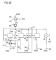
- FIG. 3E shows a further exemplary embodiment of the Hall sensor assembly 10, which is a development of the Hall sensor arrangements shown in Figures 1A, 2A, 2B, 3A, 3B and 3D is.
- the Hall sensor arrangement 10 has a voltage source 42, which is connected to the supply terminals of the Hall sensor 11 and the detection unit 13.
- the voltage source 42 is realized as a constant voltage source.
- the voltage source 42 is connected via the Hall sensor 11 and the signal source 12 to a reference potential terminal 36.
- the signal source 12, the Hall element 14 and the input circuit 15 are arranged between an output of the voltage source 42 and the reference potential terminal 36.
- the Hall element 14 is connected via the output circuit 16, the amplifier 18 and the analog-to-digital converter 34 to the signal input of the detection unit 13.
- the voltage source 42 provides a supply voltage VD on the output side.
- the supply voltage VD is supplied to the Hall sensor 11 and the detection unit 13 to the power supply.
- a reference potential VSS can be tapped.
- At the supply voltage terminal 44 is another supply voltage VDD.
- the coil current IC provided by the current generator 31 flows from the supply voltage terminal 44 via the node 43 to the Hall sensor 11 and thus to the Hall element 14.
- the voltage source 42 serves as a load balance.
- the coil current IC flow partially or completely through the Hall element 14.
- the efficiency of the Hall sensor assembly 10 is increased.
- the Hall sensor 11 comprises a first number M Hall elements. This is by the number M of lines between the node 43 and the Hall element 14 in FIG. 3E indicated.
- FIG. 4A shows an exemplary embodiment of details of a Hall sensor assembly 10, which is a development of the Hall sensor arrangements shown in the above figures.
- the signal source 12 comprises the current source 32 and a further current source 50.
- the current source 32 and the further current source 50 are connected in parallel.
- An output of the current source 32 and an output of the further current source 50 are connected to the output of the signal source 12.
- the Hall element 14 has a first, second, third and fourth connection 51 to 54.
- the Hall element 14 is realized symmetrically.
- the first terminal 51 faces the third terminal 53. Accordingly, the second terminal is opposite to the fourth terminal 55.
- the input circuit 15 comprises a first and a second multiplexer 55, 56.
- the output circuit 16 comprises a third and a fourth multiplexer 57, 58.
- the first, second, third and fourth multiplexers 55 to 58 each have four inputs connected to the first, second, third and fourth terminals 51 to 54 of the Hall element 14 are coupled.
- An output of the first multiplexer 55 is connected to the reference potential terminal 36.
- An output of the second multiplexer 56 is connected to the output of the signal source 12 via the input of the Hall sensor 11.
- An output of the third multiplexer 57 and an output of the fourth multiplexer 58 are coupled to the amplifier 18.
- the amplifier 18 has a first and a second input 59, 60.
- the first input 59 is connected to the output of the third multiplexer 57 and the second input 60 is connected to the output of the fourth multiplexer 58.
- the current source 32 and the further current source 50 are each implemented as constant current sources.
- the current source 32 and the further current source 50 are each separately switched on and off.
- the current source 32 outputs a first current value IP1, which corresponds to the first value I1 of the input signal I.
- the further current source 50 outputs a second current value IP2.
- the sum of the first and the second current value IP1, IP2 corresponds to the second value 12 of the input signal I.
- the current source 32 and the further current source 50 are thus switched on.
- the signal source 12 generates the first and second values I1, 12 of the input signal I according to the first embodiment of the method.
- the detection unit 13 provides four multiplexer control signals S1 to S4 to be supplied to the first, second, third and fourth multiplexers 55 to 58.
- the Current Spinning technique also called Current Spinning method or current rotation method implemented.
- One cycle of the current spinning technique has at least two phases.
- Two opposite terminals of the Hall element 14 are coupled via the first and the second multiplexer 55, 56 to the reference potential terminal 36 and to the output of the signal source 12, respectively. Accordingly, the two further terminals of the Hall element 14 via the third and the fourth multiplexer 57, 58 are coupled to the first and the second input 59, 60 of the amplifier 18.
- the Hall element 14 is sensitive to a magnetic field perpendicular to the surface.
- the output signal V of the Hall sensor 11 is only after complete passage through the phases of a cycle of the current Spinning technique provided. During the phases of a cycle of the current spinning technique, the value of the input signal I is constant. To determine the output signal V at the first value I1 of the input signal I, all phases of the cycle are run according to the current spinning technique. Accordingly, in order to determine the output signal V at the second and / or the third value 12, 13 of the input signal I, the phases of a cycle of the current spinning technique are likewise completely traversed.
- a cycle may have four phases.
- the current spinning technique it is achieved that the current flow in the Hall element 14 assumes four different directions.
- the amount of the sensor signal VS is equal without any offset in all four phases of the current spinning technique.
- each of the four terminals 51 to 54 of the Hall element 14 is thus connected in phase with the output of the signal source 12, the reference potential terminal 36, the first input 59 and the second input 60 of the amplifier 18.
- the sensor signal VS is implemented as a differential signal.
- the sensor signal VS can be tapped between two terminals of the Hall element 14.
- the sensor signal VS is supplied to the first and the second input 59, 60 of the amplifier 18.
- the amplifier 18 converts the sensor signal VS into an amplified sensor signal AV.
- the amplified sensor signal AV is related to the reference potential VSS at the reference potential terminal 36.
- one of the six above-described embodiments of the method according to the proposed principle is performed in addition to the current spinning technique.
- the combination of the current spinning technique and one of the explained six embodiments of the method causes a high accuracy of the magnetic field determination.
- the second current value IP2 corresponds to the second value 12 of the input signal.
- the current source 32 and the further current source 50 are thus switched on individually.
- the current source 32 and the further current source 50 are switched on simultaneously.
- the sum of the first and the second current value IP1, IP2 corresponds to the third value 13 of the input signal I.
- the three different values I1, 12, 13 of the input signal I can be efficiently generated with two current sources 32, 50.
- the signal source 12 comprises an additional current source whose output is connected to the output of the signal source 12.
- one cycle of the current spinning technique comprises exactly two phases. In this case, in a first phase, the first terminal 51 of the Hall element 14 is coupled to the reference potential terminal 36 and the third terminal 53 of the Hall element 14 to the output of the signal source 12 via the first and the second multiplexer 55, 56. In the second phase, the first terminal 51 is coupled to the output of the signal source 12 and the third terminal 53 is coupled to the reference potential terminal 36.
- the second and the fourth connection 52, 54 of the Hall element 14 are alternately coupled to the first and the second input 59, 60 of the amplifier 36 via the third and the fourth multiplexer 57, 58 in the first and the second phase. In the two phases of the cycle thus becomes the direction of the current flowing through the Hall element 14 is rotated by 180 degrees.
- the Hall element 14 comprises further terminals, which are coupled to the signal source 12 and the amplifier 18 by means of the four multiplexers 55 to 58.
- a cycle for operating such a Hall element 14 may have more than four phases.
- FIG. 4B shows another exemplary embodiment of a detail of the Hall sensor 11.
- the Hall sensor 11 includes the Hall element 14 and another Hall element 61.
- the Hall element 14 and the further Hall element 61 are connected according to the principle of geometric spinning.
- the Hall element 14 and the further Hall element 61 are fixedly connected as Hall element pair and can be used instead of the Hall element 14 in one of the above-described Hall sensor arrangements.
- the Hall element 14 and the further Hall element 61 are both coupled to the output of the signal source 12 and the amplifier 18.
- the direction of the current flow through the Hall element 14 has an angle to the direction of the current flow through the further Hall element 61. Preferably, the angle is 45 ° or 90 °.
- the outputs of the Hall element 14 and the further Hall element 61 are connected in parallel.
- the Hall element pair comprising the Hall element 14 and the further Hall element 61, has four terminals 62 to 65.
- a first terminal 62 is connected to the output of the signal source 12, a second terminal 63 to the reference potential terminal 36, a third terminal 64 to the first input 59 of the amplifier 18 and a fourth terminal 65 to the second input 60 of the amplifier 18 is connected.
- the Hall element 14 and the further Hall element 61 have a parallel circuit with respect to the input signals I and the sensor signals VS.
- the first and third terminals 51, 53 of the Hall element 14 are permanently connected to a first and a third terminal 51 ', 53' of the further Hall element 61.
- the second and the fourth connection 52, 54 of the Hall element 14 are permanently connected to a second or a fourth connection 52 ', 54' of the further Hall element 61. Consequently, the input signal terminals 51, 53, 51 ', 53' of the two Hall elements 14, 61 are connected in parallel. Further, the output signal terminals 52, 54, 52 ', 54' of the two Hall elements 14, 61 are connected in parallel.
- the input signal I can be designed as current or voltage.
- the input circuit 15 and the output circuit 16 couples the Hall element pair with the signal source 12 and the amplifier 18.
- the four terminals 62 to 65 of the Hall element pair via the first, second, third and fourth multiplexer 57 to 58 the output of the signal source 12, the reference potential terminal 36 and the first and the second input 59, 60 of the amplifier 18 according to the two or four phases of the current spinning technique connected.
- At least one additional Hall element may be connected to the Hall element 14 and the further Hall element 61 according to the principle of geometric spinning.
- the Hall sensor 11 four Hall elements 14, 61, which together are connected.
Landscapes
- Physics & Mathematics (AREA)
- Condensed Matter Physics & Semiconductors (AREA)
- General Physics & Mathematics (AREA)
- Measuring Magnetic Variables (AREA)
- Hall/Mr Elements (AREA)
- Transmission And Conversion Of Sensor Element Output (AREA)
Claims (15)
- Procédé destiné à exploiter un ensemble capteur à effet Hall, comprenant:- réglage d'au moins deux valeurs (I1, 12) numériquement différentes d'un signal d'entrée (I) d'un capteur à effet Hall (11) de l'ensemble capteur à effet Hall (10) et détermination des valeurs associées (V1, V2) d'un signal de sortie (V) du capteur à effet Hall (11), sachant que le signal de sortie (V) n'est mis à disposition qu'après déroulement complet des phases d'un cycle de la technique de Current Spinning et la valeur du signal d'entrée (I) est constante pendant les phases du cycle de la technique de Current Spinning, ainsi que- détermination d'une valeur de décalage résiduelle (k, VOFF) du signal de sortie (V) en fonction des valeurs (V1, V2) du signal de sortie (V) qui ont été déterminées pour les au moins deux valeurs (I1, 12) du signal d'entrée (I).
- Procédé selon la revendication 1,
dans lequel le signal d'entrée (I) est réalisé comme courant ou tension. - Procédé selon la revendication 1 ou 2,
dans lequel les au moins deux valeurs (I1, 12) du signal d'entrée (I) ou un facteur de mise à l'échelle (α2, α3) entre deux valeurs issues de l'ensemble des au moins deux valeurs (I1, 12) du signal d'entrée (I) sont pris en compte lors de la détermination de la valeur de décalage résiduelle (k, VOFF). - Procédé selon l'une des revendications 1 à 3,
dans lequel l'ensemble capteur à effet Hall (10) est calibré en exploitation, sachant qu'une phase de calibrage dans laquelle la valeur de décalage résiduelle (k, VOFF) est déterminée, est intercalée entre deux phases d'exploitation dans lesquelles la valeur d'un champ magnétique (B) est déterminée en fonction de la valeur de décalage résiduelle (k, VOFF). - Procédé selon l'une des revendications 1 à 4,
dans lequel l'ensemble capteur à effet Hall (10) est calibré en présence d'un champ magnétique (B) externe qui présente une intensité de champ magnétique inconnue. - Procédé selon l'une des revendications 1 à 5,
dans lequel la valeur de décalage résiduelle est un facteur de décalage (k) ou une tension de décalage résiduelle (VOFF) et le facteur de décalage (k) et la tension de décalage résiduelle (VOFF) sont calculés d'après l'équation suivante:
VOFF étant la valeur de la tension de décalage résiduelle, k la valeur du facteur de décalage, I la valeur du signal d'entrée et n la valeur d'un exposant. - Procédé selon la revendication 6,
dans lequel la valeur de l'exposant (n) est spécifiée. - Procédé selon la revendication 6,
dans lequel la valeur de l'exposant (n) est déterminée moyennant réglage d'au moins trois valeurs (I1, 12, 13) numériquement différentes du signal d'entrée (I) et détermination des valeurs associées (V1, V2, V3) du signal de sortie (V) du capteur à effet Hall (11). - Procédé selon l'une des revendications 1 à 8,
dans lequel la valeur d'un champ magnétique (B) est déterminée d'après l'équation suivante:
V étant la valeur du signal de sortie, B la valeur du champ magnétique, S la valeur d'une sensibilité, I la valeur du signal d'entrée et VOFF la valeur d'une tension de décalage résiduelle. - Procédé selon la revendication 9,
dans lequel la valeur de la sensibilité (S) est spécifiée ou dans lequel une bobine (30) est disposée de telle façon par rapport au capteur à effet Hall (11) que le champ magnétique de la bobine (30) influence le champ magnétique détecté par le capteur à effet Hall (11), et la valeur de la sensibilité (S) est déterminée au moyen de la bobine (30) pour les au moins deux valeurs (I1, 12) du signal d'entrée (I). - Procédé selon l'une des revendications 1 à 10,
dans lequel une bobine (30) est disposée de telle façon par rapport au capteur à effet Hall (11) que le champ magnétique de la bobine (30) influence le champ magnétique (B) détecté par le capteur à effet Hall (11), et, dans une phase d'exploitation, la valeur d'un courant de bobine (IC) est réglée en fonction de la valeur de décalage résiduelle (k, VOFF). - Procédé selon l'une des revendications 1 à 10,
dans lequel une bobine (30) est disposée de telle façon par rapport au capteur à effet Hall (11) que le champ magnétique de la bobine (30) influence le champ magnétique (B) détecté par le capteur à effet Hall (11), et, dans une phase d'exploitation, la valeur d'un courant de bobine (IC) est réglée de telle façon que le signal de sortie (V) prenne approximativement la valeur 0. - Procédé selon la revendication 12,
dans lequel la bobine (30) est couplée de telle façon au capteur à effet Hall (11) que le courant de bobine (IC) passe comme signal d'entrée (I) à travers le capteur à effet Hall (11). - Ensemble capteur à effet Hall, comprenant:- un capteur à effet Hall, comprenant- un élément à effet Hall (14),- un circuit d'entrée (15) qui relie une entrée du capteur à effet Hall (11) à l'élément à effet Hall (14),- un circuit de sortie (16) et un circuit d'évaluation (17) qui relient l'élément à effet Hall (14) à une sortie du capteur à effet Hall (11), sachant qu'un signal de sortie (V) mis à disposition par le circuit d'évaluation (17) n'est mis à disposition qu'après déroulement complet des phases d'un cycle de la technique de Current Spinning,- une source de signal (12) qui est couplée à l'entrée du capteur à effet Hall (11), et- une unité de détermination (13) qui est couplée à la sortie du capteur à effet Hall (11),
caractérisé en ce que
la source de signal (12) est configurée pour mettre à disposition au moins deux valeurs (I1, 12) numériquement différentes d'un signal d'entrée (I) du capteur à effet Hall (11), sachant que la valeur du signal d'entrée (I) est constante pendant les phases du cycle de la technique de Current Spinning, et- l'unité de détermination (13) est configurée pour déterminer une valeur de décalage résiduelle (k, VOFF) d'un signal de sortie (V) du capteur à effet Hall (11) en fonction des valeurs (V1, V2) du signal de sortie (V) qui sont déterminées pour les au moins deux valeurs (I1, 12) du signal d'entrée (I). - Ensemble capteur à effet Hall selon la revendication 14, comprenant une bobine (30) qui est fermement reliée au capteur à effet Hall (11) et disposée de telle façon par rapport au capteur à effet Hall (11) que le champ magnétique (B) détectable par le capteur à effet Hall (11) soit influençable par le champ magnétique de la bobine (30).
Applications Claiming Priority (2)
| Application Number | Priority Date | Filing Date | Title |
|---|---|---|---|
| DE102011102483A DE102011102483A1 (de) | 2011-05-24 | 2011-05-24 | Verfahren zum Betreiben einer Hallsensoranordnung und Hallsensoranordnung |
| PCT/EP2012/059728 WO2012160143A2 (fr) | 2011-05-24 | 2012-05-24 | Procédé de fonctionnement d'un ensemble capteur à effet hall et ensemble capteur à effet hall |
Publications (2)
| Publication Number | Publication Date |
|---|---|
| EP2715384A2 EP2715384A2 (fr) | 2014-04-09 |
| EP2715384B1 true EP2715384B1 (fr) | 2015-07-15 |
Family
ID=46320900
Family Applications (1)
| Application Number | Title | Priority Date | Filing Date |
|---|---|---|---|
| EP12728424.8A Active EP2715384B1 (fr) | 2011-05-24 | 2012-05-24 | Procédé de fonctionnement d'un ensemble capteur à effet hall et ensemble capteur à effet hall |
Country Status (4)
| Country | Link |
|---|---|
| US (1) | US9551765B2 (fr) |
| EP (1) | EP2715384B1 (fr) |
| DE (1) | DE102011102483A1 (fr) |
| WO (1) | WO2012160143A2 (fr) |
Families Citing this family (48)
| Publication number | Priority date | Publication date | Assignee | Title |
|---|---|---|---|---|
| US9823090B2 (en) | 2014-10-31 | 2017-11-21 | Allegro Microsystems, Llc | Magnetic field sensor for sensing a movement of a target object |
| US9817078B2 (en) | 2012-05-10 | 2017-11-14 | Allegro Microsystems Llc | Methods and apparatus for magnetic sensor having integrated coil |
| GB201217293D0 (en) * | 2012-09-27 | 2012-11-14 | Texas Instruments Deutschland | Improvements on or relating to sensing arrangements |
| US10725100B2 (en) | 2013-03-15 | 2020-07-28 | Allegro Microsystems, Llc | Methods and apparatus for magnetic sensor having an externally accessible coil |
| US9810519B2 (en) | 2013-07-19 | 2017-11-07 | Allegro Microsystems, Llc | Arrangements for magnetic field sensors that act as tooth detectors |
| US10145908B2 (en) | 2013-07-19 | 2018-12-04 | Allegro Microsystems, Llc | Method and apparatus for magnetic sensor producing a changing magnetic field |
| US10495699B2 (en) * | 2013-07-19 | 2019-12-03 | Allegro Microsystems, Llc | Methods and apparatus for magnetic sensor having an integrated coil or magnet to detect a non-ferromagnetic target |
| US9389295B2 (en) | 2013-09-10 | 2016-07-12 | Fisher Controls International Llc | Hall effect sensor system with diagnostic capabilities |
| GB201319627D0 (en) | 2013-11-06 | 2013-12-18 | Melexis Technologies Nv | Hall sensor readout system with offset determination using the hall element itself |
| US10712403B2 (en) | 2014-10-31 | 2020-07-14 | Allegro Microsystems, Llc | Magnetic field sensor and electronic circuit that pass amplifier current through a magnetoresistance element |
| US9823092B2 (en) | 2014-10-31 | 2017-11-21 | Allegro Microsystems, Llc | Magnetic field sensor providing a movement detector |
| US9720054B2 (en) | 2014-10-31 | 2017-08-01 | Allegro Microsystems, Llc | Magnetic field sensor and electronic circuit that pass amplifier current through a magnetoresistance element |
| US9719806B2 (en) | 2014-10-31 | 2017-08-01 | Allegro Microsystems, Llc | Magnetic field sensor for sensing a movement of a ferromagnetic target object |
| US10126348B2 (en) * | 2015-04-29 | 2018-11-13 | ZTZ Service International, Inc. | Combined on-line bushing monitoring and geo-magnetic induced current monitoring system |
| US11402440B2 (en) * | 2015-07-17 | 2022-08-02 | Allegro Microsystems, Llc | Methods and apparatus for trimming a magnetic field sensor |
| US10012518B2 (en) | 2016-06-08 | 2018-07-03 | Allegro Microsystems, Llc | Magnetic field sensor for sensing a proximity of an object |
| US10260905B2 (en) | 2016-06-08 | 2019-04-16 | Allegro Microsystems, Llc | Arrangements for magnetic field sensors to cancel offset variations |
| US10041810B2 (en) | 2016-06-08 | 2018-08-07 | Allegro Microsystems, Llc | Arrangements for magnetic field sensors that act as movement detectors |
| DE102016225305B4 (de) * | 2016-12-16 | 2019-07-11 | Fraunhofer-Gesellschaft zur Förderung der angewandten Forschung e.V. | Verfahren zur Offset-Kompensation eines Sensorsignals eines Hall-Sensors und Sensoranordnung |
| US10996289B2 (en) | 2017-05-26 | 2021-05-04 | Allegro Microsystems, Llc | Coil actuated position sensor with reflected magnetic field |
| US10324141B2 (en) | 2017-05-26 | 2019-06-18 | Allegro Microsystems, Llc | Packages for coil actuated position sensors |
| US10837943B2 (en) | 2017-05-26 | 2020-11-17 | Allegro Microsystems, Llc | Magnetic field sensor with error calculation |
| US10310028B2 (en) | 2017-05-26 | 2019-06-04 | Allegro Microsystems, Llc | Coil actuated pressure sensor |
| US11428755B2 (en) | 2017-05-26 | 2022-08-30 | Allegro Microsystems, Llc | Coil actuated sensor with sensitivity detection |
| US10641842B2 (en) | 2017-05-26 | 2020-05-05 | Allegro Microsystems, Llc | Targets for coil actuated position sensors |
| JP6620796B2 (ja) * | 2017-07-28 | 2019-12-18 | Tdk株式会社 | オフセット推定装置および方法、磁気センサの補正装置ならびに電流センサ |
| JP2019062450A (ja) * | 2017-09-27 | 2019-04-18 | 日本電産株式会社 | 演算回路、制御回路及び表示装置姿勢検出システム |
| EP3467443B1 (fr) | 2017-10-05 | 2021-08-18 | ams AG | Capteur de position et procédé de détection et de diagnostic de position |
| US10866117B2 (en) | 2018-03-01 | 2020-12-15 | Allegro Microsystems, Llc | Magnetic field influence during rotation movement of magnetic target |
| US11255700B2 (en) | 2018-08-06 | 2022-02-22 | Allegro Microsystems, Llc | Magnetic field sensor |
| DE102018128469B4 (de) * | 2018-11-14 | 2020-11-12 | Senis Ag | Magnetfeldsensor mit geringem Rauschen und hoher Bandbreite |
| US10732164B2 (en) | 2018-12-12 | 2020-08-04 | ZTZ Service International, Inc. | System and method for headspace monitoring in transformers |
| US10823586B2 (en) | 2018-12-26 | 2020-11-03 | Allegro Microsystems, Llc | Magnetic field sensor having unequally spaced magnetic field sensing elements |
| US11061084B2 (en) | 2019-03-07 | 2021-07-13 | Allegro Microsystems, Llc | Coil actuated pressure sensor and deflectable substrate |
| US10955306B2 (en) | 2019-04-22 | 2021-03-23 | Allegro Microsystems, Llc | Coil actuated pressure sensor and deformable substrate |
| US11061100B2 (en) * | 2019-06-12 | 2021-07-13 | Texas Instruments Incorporated | System for continuous calibration of hall sensors |
| US11867773B2 (en) | 2019-06-18 | 2024-01-09 | Texas Instruments Incorporated | Switched capacitor integrator circuit with reference, offset cancellation and differential to single-ended conversion |
| US11280637B2 (en) | 2019-11-14 | 2022-03-22 | Allegro Microsystems, Llc | High performance magnetic angle sensor |
| US11237020B2 (en) | 2019-11-14 | 2022-02-01 | Allegro Microsystems, Llc | Magnetic field sensor having two rows of magnetic field sensing elements for measuring an angle of rotation of a magnet |
| US11262422B2 (en) | 2020-05-08 | 2022-03-01 | Allegro Microsystems, Llc | Stray-field-immune coil-activated position sensor |
| RU2762021C1 (ru) * | 2021-02-16 | 2021-12-14 | Открытое акционерное общество "Севернефтегазпром" | Система диагностики датчиков холла и способ ее применения |
| US11493361B2 (en) | 2021-02-26 | 2022-11-08 | Allegro Microsystems, Llc | Stray field immune coil-activated sensor |
| US11578997B1 (en) | 2021-08-24 | 2023-02-14 | Allegro Microsystems, Llc | Angle sensor using eddy currents |
| CN114383495B (zh) * | 2021-11-15 | 2023-11-03 | 北京诺多科技发展有限公司 | 一种双霍尔偏航角度测量方法 |
| US12153101B2 (en) | 2022-01-27 | 2024-11-26 | Nxp Usa, Inc. | Sensor calibration circuit |
| DE102023122076A1 (de) * | 2023-08-17 | 2025-02-20 | Infineon Technologies Ag | Selbstkalibrierendes stromsensor-package |
| US12523717B2 (en) | 2024-02-15 | 2026-01-13 | Allegro Microsystems, Llc | Closed loop magnetic field sensor with current control |
| CN118541016B (zh) * | 2024-07-22 | 2024-11-12 | 苏州矩阵光电有限公司 | 低零点偏移低漂移的双霍尔集成芯片及电流传感器元件 |
Family Cites Families (13)
| Publication number | Priority date | Publication date | Assignee | Title |
|---|---|---|---|---|
| DE4302342A1 (en) * | 1992-01-28 | 1993-07-29 | El Mos Elektronik In Mos Techn | Offset compensated measurement of magnetic field with Hall element - involves chip-internal electronic compensation with two measurement phases between which measurement and supply connections are interchanged |
| DE4431703C2 (de) * | 1994-09-06 | 1997-01-30 | Itt Ind Gmbh Deutsche | Magnetfeldsensor mit Hallelement |
| EP0859964B1 (fr) | 1996-09-09 | 2006-11-15 | AMS International AG | Procede de reduction de la tension de decalage d'un dispositif hall |
| US6064202A (en) | 1997-09-09 | 2000-05-16 | Physical Electronics Laboratory | Spinning current method of reducing the offset voltage of a hall device |
| DE19910411C2 (de) * | 1999-03-10 | 2001-08-30 | Daimler Chrysler Ag | Verfahren und Vorrichtung zur Offset-kompensierten Magnetfeldmessung mittels eines Hallsensors |
| DE19943128A1 (de) | 1999-09-09 | 2001-04-12 | Fraunhofer Ges Forschung | Hall-Sensoranordnung zur Offset-kompensierten Magnetfeldmessung |
| JP4601892B2 (ja) | 2002-07-04 | 2010-12-22 | ラムバス・インコーポレーテッド | 半導体装置および半導体チップのバンプ製造方法 |
| DE10313642A1 (de) * | 2003-03-26 | 2004-10-14 | Micronas Gmbh | Offset-reduzierter Hall-sensor |
| NL1025089C2 (nl) * | 2003-12-19 | 2005-06-21 | Xensor Integration B V | Magneetveldsensor, drager van een dergelijke magneetveldsensor en een kompas, voorzien van een dergelijke magneetveldsensor. |
| DE102004021863A1 (de) | 2004-05-04 | 2005-12-01 | Infineon Technologies Ag | Sensorelement zum Bereitstellen eines Sensorsignals und Verfahren zum Betreiben eines Sensorelementes |
| GB0620307D0 (en) * | 2006-10-16 | 2006-11-22 | Ami Semiconductor Belgium Bvba | Auto-calibration of magnetic sensor |
| DE102007044471A1 (de) | 2007-09-18 | 2009-04-02 | Fraunhofer-Gesellschaft zur Förderung der angewandten Forschung e.V. | Verfahren zur abschnittsweisen Bestimmung eines parameterabhängigen Korrekturwertnäherungsverlaufs und Sensoranordnung |
| US8154281B2 (en) * | 2008-04-17 | 2012-04-10 | Infineon Technologies Ag | Sensor system wherein spinning phases of the spinning current hall sensor are lengthened in residual offset adjustment |
-
2011
- 2011-05-24 DE DE102011102483A patent/DE102011102483A1/de not_active Withdrawn
-
2012
- 2012-05-24 EP EP12728424.8A patent/EP2715384B1/fr active Active
- 2012-05-24 WO PCT/EP2012/059728 patent/WO2012160143A2/fr not_active Ceased
- 2012-05-24 US US14/119,183 patent/US9551765B2/en active Active
Also Published As
| Publication number | Publication date |
|---|---|
| EP2715384A2 (fr) | 2014-04-09 |
| US20140163911A1 (en) | 2014-06-12 |
| WO2012160143A2 (fr) | 2012-11-29 |
| US9551765B2 (en) | 2017-01-24 |
| WO2012160143A3 (fr) | 2013-03-28 |
| DE102011102483A1 (de) | 2012-11-29 |
Similar Documents
| Publication | Publication Date | Title |
|---|---|---|
| EP2715384B1 (fr) | Procédé de fonctionnement d'un ensemble capteur à effet hall et ensemble capteur à effet hall | |
| DE112012005548B4 (de) | Ausgangswertkorrekturverfahren für eine Sensorvorrichtung für eine physikalische Grösse, Ausgangskorrekturverfahren für einen Sensor für eine physikalische Grösse, Sensorvorrichtung für eine physikalische Grösse und Ausgangswertkorrekturvorrichtung für einen Sensor für eine physikalische Grösse | |
| EP2567223B1 (fr) | Dispositif de mesure de la conductibilité électrique d'un milieu liquide | |
| DE10156027B4 (de) | Abgleichbare Filterschaltung | |
| DE68907628T2 (de) | Elektromagnetischer durchflussmesser zur gleichzeitigen messung des durchflusses und der leitfaehigkeit einer fluessigkeit. | |
| DE10131229B4 (de) | Eine physikalische Größe erfassender Sensor | |
| EP1616174B1 (fr) | Procede permettant de faire fonctionner un detecteur de gaz | |
| DE102014107499A1 (de) | Kalibriertes Temperaturmesssystem | |
| DE102007047887A1 (de) | Kapazitätserfassungsvorrichtung | |
| DE69014927T2 (de) | Speiseschaltung und Brücken-Messanordnung mit einer Ausgangssignalausgleichsschaltung. | |
| DE102014107504A1 (de) | Eingangsstufe für temperaturmesssystem | |
| DE102005045635B4 (de) | Anordnung und Verfahren zur Bereitstellung eines temperaturabhängigen Signals | |
| WO2004102211A1 (fr) | Ensemble circuit de commutation pour la stabilisation de potentiel sur un biocapteur et la numerisation du courant de mesure | |
| EP2666023A1 (fr) | Dispositif de mesure de courant | |
| DE102010028718A1 (de) | Erfassung eines dielektrischen Objekts | |
| DE102015002123B4 (de) | Magnetfelderfassungsvorrichtung | |
| DE10204652B4 (de) | Schaltkreis-Anordnung, elektrochemischer Sensor, Sensor-Anordnung und Verfahren zum Verarbeiten eines über eine Sensor-Elektrode bereitgestellten Stromsignals | |
| DE69615271T2 (de) | Schaltung zur Eingabe eines Analogsignals mit einem Analog-Digital-Wandler in einer Halbleiterschaltung | |
| EP1512021B1 (fr) | Montage et procede pour compenser les variations d'un facteur de transmission d'un systeme de detection de champ magnetique | |
| DE3642771A1 (de) | Verfahren und vorrichtung zur messung der messgroesse eines messobjekts | |
| EP1599737A1 (fr) | Procede et circuit pour la determination d'une valeur de mesure electrique relative a un element de resistance, de preference pour la determination d'un courant electrique traversant un tel element de resistance | |
| EP2233890A2 (fr) | Capteur capacitif et procédé de détection capacitive de l'écartement d'un objet | |
| DE19947301C1 (de) | Vorrichtung und Verfahren zur Kalibrierung von Sensoren | |
| DE102016113283B4 (de) | Verfahren zum Bestimmen einer Widerstandsauslenkung einer Wheatstone-Brücke in einer Hochtemperaturumgebung und Anordnung zum Erfassen eines Druckes mit einer Druckmembran | |
| EP2174146B1 (fr) | Ensemble et procédé pour la mesure d'un courant circulant dans un conducteur électrique |
Legal Events
| Date | Code | Title | Description |
|---|---|---|---|
| PUAI | Public reference made under article 153(3) epc to a published international application that has entered the european phase |
Free format text: ORIGINAL CODE: 0009012 |
|
| 17P | Request for examination filed |
Effective date: 20131022 |
|
| AK | Designated contracting states |
Kind code of ref document: A2 Designated state(s): AL AT BE BG CH CY CZ DE DK EE ES FI FR GB GR HR HU IE IS IT LI LT LU LV MC MK MT NL NO PL PT RO RS SE SI SK SM TR |
|
| DAX | Request for extension of the european patent (deleted) | ||
| GRAP | Despatch of communication of intention to grant a patent |
Free format text: ORIGINAL CODE: EPIDOSNIGR1 |
|
| INTG | Intention to grant announced |
Effective date: 20150213 |
|
| GRAS | Grant fee paid |
Free format text: ORIGINAL CODE: EPIDOSNIGR3 |
|
| GRAA | (expected) grant |
Free format text: ORIGINAL CODE: 0009210 |
|
| AK | Designated contracting states |
Kind code of ref document: B1 Designated state(s): AL AT BE BG CH CY CZ DE DK EE ES FI FR GB GR HR HU IE IS IT LI LT LU LV MC MK MT NL NO PL PT RO RS SE SI SK SM TR |
|
| REG | Reference to a national code |
Ref country code: CH Ref legal event code: EP Ref country code: GB Ref legal event code: FG4D Free format text: NOT ENGLISH |
|
| REG | Reference to a national code |
Ref country code: IE Ref legal event code: FG4D Free format text: LANGUAGE OF EP DOCUMENT: GERMAN |
|
| REG | Reference to a national code |
Ref country code: AT Ref legal event code: REF Ref document number: 737072 Country of ref document: AT Kind code of ref document: T Effective date: 20150815 |
|
| REG | Reference to a national code |
Ref country code: DE Ref legal event code: R096 Ref document number: 502012003815 Country of ref document: DE |
|
| REG | Reference to a national code |
Ref country code: NL Ref legal event code: MP Effective date: 20150715 |
|
| REG | Reference to a national code |
Ref country code: LT Ref legal event code: MG4D |
|
| PG25 | Lapsed in a contracting state [announced via postgrant information from national office to epo] |
Ref country code: NO Free format text: LAPSE BECAUSE OF FAILURE TO SUBMIT A TRANSLATION OF THE DESCRIPTION OR TO PAY THE FEE WITHIN THE PRESCRIBED TIME-LIMIT Effective date: 20151015 Ref country code: GR Free format text: LAPSE BECAUSE OF FAILURE TO SUBMIT A TRANSLATION OF THE DESCRIPTION OR TO PAY THE FEE WITHIN THE PRESCRIBED TIME-LIMIT Effective date: 20151016 Ref country code: LT Free format text: LAPSE BECAUSE OF FAILURE TO SUBMIT A TRANSLATION OF THE DESCRIPTION OR TO PAY THE FEE WITHIN THE PRESCRIBED TIME-LIMIT Effective date: 20150715 Ref country code: FI Free format text: LAPSE BECAUSE OF FAILURE TO SUBMIT A TRANSLATION OF THE DESCRIPTION OR TO PAY THE FEE WITHIN THE PRESCRIBED TIME-LIMIT Effective date: 20150715 Ref country code: LV Free format text: LAPSE BECAUSE OF FAILURE TO SUBMIT A TRANSLATION OF THE DESCRIPTION OR TO PAY THE FEE WITHIN THE PRESCRIBED TIME-LIMIT Effective date: 20150715 |
|
| PG25 | Lapsed in a contracting state [announced via postgrant information from national office to epo] |
Ref country code: PL Free format text: LAPSE BECAUSE OF FAILURE TO SUBMIT A TRANSLATION OF THE DESCRIPTION OR TO PAY THE FEE WITHIN THE PRESCRIBED TIME-LIMIT Effective date: 20150715 Ref country code: ES Free format text: LAPSE BECAUSE OF FAILURE TO SUBMIT A TRANSLATION OF THE DESCRIPTION OR TO PAY THE FEE WITHIN THE PRESCRIBED TIME-LIMIT Effective date: 20150715 Ref country code: RS Free format text: LAPSE BECAUSE OF FAILURE TO SUBMIT A TRANSLATION OF THE DESCRIPTION OR TO PAY THE FEE WITHIN THE PRESCRIBED TIME-LIMIT Effective date: 20150715 Ref country code: HR Free format text: LAPSE BECAUSE OF FAILURE TO SUBMIT A TRANSLATION OF THE DESCRIPTION OR TO PAY THE FEE WITHIN THE PRESCRIBED TIME-LIMIT Effective date: 20150715 Ref country code: PT Free format text: LAPSE BECAUSE OF FAILURE TO SUBMIT A TRANSLATION OF THE DESCRIPTION OR TO PAY THE FEE WITHIN THE PRESCRIBED TIME-LIMIT Effective date: 20151116 Ref country code: SE Free format text: LAPSE BECAUSE OF FAILURE TO SUBMIT A TRANSLATION OF THE DESCRIPTION OR TO PAY THE FEE WITHIN THE PRESCRIBED TIME-LIMIT Effective date: 20150715 |
|
| REG | Reference to a national code |
Ref country code: DE Ref legal event code: R097 Ref document number: 502012003815 Country of ref document: DE |
|
| PG25 | Lapsed in a contracting state [announced via postgrant information from national office to epo] |
Ref country code: CZ Free format text: LAPSE BECAUSE OF FAILURE TO SUBMIT A TRANSLATION OF THE DESCRIPTION OR TO PAY THE FEE WITHIN THE PRESCRIBED TIME-LIMIT Effective date: 20150715 Ref country code: DK Free format text: LAPSE BECAUSE OF FAILURE TO SUBMIT A TRANSLATION OF THE DESCRIPTION OR TO PAY THE FEE WITHIN THE PRESCRIBED TIME-LIMIT Effective date: 20150715 Ref country code: SK Free format text: LAPSE BECAUSE OF FAILURE TO SUBMIT A TRANSLATION OF THE DESCRIPTION OR TO PAY THE FEE WITHIN THE PRESCRIBED TIME-LIMIT Effective date: 20150715 Ref country code: EE Free format text: LAPSE BECAUSE OF FAILURE TO SUBMIT A TRANSLATION OF THE DESCRIPTION OR TO PAY THE FEE WITHIN THE PRESCRIBED TIME-LIMIT Effective date: 20150715 Ref country code: IT Free format text: LAPSE BECAUSE OF FAILURE TO SUBMIT A TRANSLATION OF THE DESCRIPTION OR TO PAY THE FEE WITHIN THE PRESCRIBED TIME-LIMIT Effective date: 20150715 |
|
| PLBE | No opposition filed within time limit |
Free format text: ORIGINAL CODE: 0009261 |
|
| STAA | Information on the status of an ep patent application or granted ep patent |
Free format text: STATUS: NO OPPOSITION FILED WITHIN TIME LIMIT |
|
| PG25 | Lapsed in a contracting state [announced via postgrant information from national office to epo] |
Ref country code: RO Free format text: LAPSE BECAUSE OF FAILURE TO SUBMIT A TRANSLATION OF THE DESCRIPTION OR TO PAY THE FEE WITHIN THE PRESCRIBED TIME-LIMIT Effective date: 20150715 |
|
| 26N | No opposition filed |
Effective date: 20160418 |
|
| PG25 | Lapsed in a contracting state [announced via postgrant information from national office to epo] |
Ref country code: IS Free format text: LAPSE BECAUSE OF FAILURE TO SUBMIT A TRANSLATION OF THE DESCRIPTION OR TO PAY THE FEE WITHIN THE PRESCRIBED TIME-LIMIT Effective date: 20150715 |
|
| PG25 | Lapsed in a contracting state [announced via postgrant information from national office to epo] |
Ref country code: SI Free format text: LAPSE BECAUSE OF FAILURE TO SUBMIT A TRANSLATION OF THE DESCRIPTION OR TO PAY THE FEE WITHIN THE PRESCRIBED TIME-LIMIT Effective date: 20150715 Ref country code: BE Free format text: LAPSE BECAUSE OF NON-PAYMENT OF DUE FEES Effective date: 20160531 |
|
| PG25 | Lapsed in a contracting state [announced via postgrant information from national office to epo] |
Ref country code: LU Free format text: LAPSE BECAUSE OF FAILURE TO SUBMIT A TRANSLATION OF THE DESCRIPTION OR TO PAY THE FEE WITHIN THE PRESCRIBED TIME-LIMIT Effective date: 20160524 |
|
| REG | Reference to a national code |
Ref country code: CH Ref legal event code: PL |
|
| GBPC | Gb: european patent ceased through non-payment of renewal fee |
Effective date: 20160524 |
|
| PG25 | Lapsed in a contracting state [announced via postgrant information from national office to epo] |
Ref country code: LI Free format text: LAPSE BECAUSE OF NON-PAYMENT OF DUE FEES Effective date: 20160531 Ref country code: CH Free format text: LAPSE BECAUSE OF NON-PAYMENT OF DUE FEES Effective date: 20160531 |
|
| REG | Reference to a national code |
Ref country code: IE Ref legal event code: MM4A |
|
| REG | Reference to a national code |
Ref country code: FR Ref legal event code: ST Effective date: 20170131 |
|
| PG25 | Lapsed in a contracting state [announced via postgrant information from national office to epo] |
Ref country code: FR Free format text: LAPSE BECAUSE OF NON-PAYMENT OF DUE FEES Effective date: 20160531 |
|
| PG25 | Lapsed in a contracting state [announced via postgrant information from national office to epo] |
Ref country code: IE Free format text: LAPSE BECAUSE OF NON-PAYMENT OF DUE FEES Effective date: 20160524 Ref country code: GB Free format text: LAPSE BECAUSE OF NON-PAYMENT OF DUE FEES Effective date: 20160524 |
|
| PG25 | Lapsed in a contracting state [announced via postgrant information from national office to epo] |
Ref country code: NL Free format text: LAPSE BECAUSE OF FAILURE TO SUBMIT A TRANSLATION OF THE DESCRIPTION OR TO PAY THE FEE WITHIN THE PRESCRIBED TIME-LIMIT Effective date: 20150715 |
|
| PG25 | Lapsed in a contracting state [announced via postgrant information from national office to epo] |
Ref country code: CY Free format text: LAPSE BECAUSE OF FAILURE TO SUBMIT A TRANSLATION OF THE DESCRIPTION OR TO PAY THE FEE WITHIN THE PRESCRIBED TIME-LIMIT Effective date: 20150715 Ref country code: HU Free format text: LAPSE BECAUSE OF FAILURE TO SUBMIT A TRANSLATION OF THE DESCRIPTION OR TO PAY THE FEE WITHIN THE PRESCRIBED TIME-LIMIT; INVALID AB INITIO Effective date: 20120524 Ref country code: SM Free format text: LAPSE BECAUSE OF FAILURE TO SUBMIT A TRANSLATION OF THE DESCRIPTION OR TO PAY THE FEE WITHIN THE PRESCRIBED TIME-LIMIT Effective date: 20150715 |
|
| PG25 | Lapsed in a contracting state [announced via postgrant information from national office to epo] |
Ref country code: TR Free format text: LAPSE BECAUSE OF FAILURE TO SUBMIT A TRANSLATION OF THE DESCRIPTION OR TO PAY THE FEE WITHIN THE PRESCRIBED TIME-LIMIT Effective date: 20150715 Ref country code: MT Free format text: LAPSE BECAUSE OF FAILURE TO SUBMIT A TRANSLATION OF THE DESCRIPTION OR TO PAY THE FEE WITHIN THE PRESCRIBED TIME-LIMIT Effective date: 20150715 Ref country code: MC Free format text: LAPSE BECAUSE OF FAILURE TO SUBMIT A TRANSLATION OF THE DESCRIPTION OR TO PAY THE FEE WITHIN THE PRESCRIBED TIME-LIMIT Effective date: 20150715 Ref country code: MK Free format text: LAPSE BECAUSE OF FAILURE TO SUBMIT A TRANSLATION OF THE DESCRIPTION OR TO PAY THE FEE WITHIN THE PRESCRIBED TIME-LIMIT Effective date: 20150715 |
|
| REG | Reference to a national code |
Ref country code: AT Ref legal event code: MM01 Ref document number: 737072 Country of ref document: AT Kind code of ref document: T Effective date: 20170524 |
|
| PG25 | Lapsed in a contracting state [announced via postgrant information from national office to epo] |
Ref country code: BG Free format text: LAPSE BECAUSE OF FAILURE TO SUBMIT A TRANSLATION OF THE DESCRIPTION OR TO PAY THE FEE WITHIN THE PRESCRIBED TIME-LIMIT Effective date: 20150715 |
|
| PG25 | Lapsed in a contracting state [announced via postgrant information from national office to epo] |
Ref country code: AT Free format text: LAPSE BECAUSE OF NON-PAYMENT OF DUE FEES Effective date: 20170524 |
|
| PG25 | Lapsed in a contracting state [announced via postgrant information from national office to epo] |
Ref country code: AL Free format text: LAPSE BECAUSE OF FAILURE TO SUBMIT A TRANSLATION OF THE DESCRIPTION OR TO PAY THE FEE WITHIN THE PRESCRIBED TIME-LIMIT Effective date: 20150715 |
|
| P01 | Opt-out of the competence of the unified patent court (upc) registered |
Effective date: 20230822 |
|
| PGFP | Annual fee paid to national office [announced via postgrant information from national office to epo] |
Ref country code: DE Payment date: 20250521 Year of fee payment: 14 |