EP2715869B1 - Dispositif d'antenne à faisceau orientable électroniquement - Google Patents
Dispositif d'antenne à faisceau orientable électroniquement Download PDFInfo
- Publication number
- EP2715869B1 EP2715869B1 EP11794262.3A EP11794262A EP2715869B1 EP 2715869 B1 EP2715869 B1 EP 2715869B1 EP 11794262 A EP11794262 A EP 11794262A EP 2715869 B1 EP2715869 B1 EP 2715869B1
- Authority
- EP
- European Patent Office
- Prior art keywords
- antenna device
- switching network
- antenna elements
- antenna
- lens
- Prior art date
- Legal status (The legal status is an assumption and is not a legal conclusion. Google has not performed a legal analysis and makes no representation as to the accuracy of the status listed.)
- Active
Links
Images



Classifications
-
- H—ELECTRICITY
- H01—ELECTRIC ELEMENTS
- H01Q—ANTENNAS, i.e. RADIO AERIALS
- H01Q19/00—Combinations of primary active antenna elements and units with secondary devices, e.g. with quasi-optical devices, for giving the antenna a desired directional characteristic
- H01Q19/06—Combinations of primary active antenna elements and units with secondary devices, e.g. with quasi-optical devices, for giving the antenna a desired directional characteristic using refracting or diffracting devices, e.g. lens
-
- H—ELECTRICITY
- H01—ELECTRIC ELEMENTS
- H01Q—ANTENNAS, i.e. RADIO AERIALS
- H01Q3/00—Arrangements for changing or varying the orientation or the shape of the directional pattern of the waves radiated from an antenna or antenna system
- H01Q3/24—Arrangements for changing or varying the orientation or the shape of the directional pattern of the waves radiated from an antenna or antenna system varying the orientation by switching energy from one active radiating element to another, e.g. for beam switching
-
- H—ELECTRICITY
- H01—ELECTRIC ELEMENTS
- H01Q—ANTENNAS, i.e. RADIO AERIALS
- H01Q19/00—Combinations of primary active antenna elements and units with secondary devices, e.g. with quasi-optical devices, for giving the antenna a desired directional characteristic
- H01Q19/06—Combinations of primary active antenna elements and units with secondary devices, e.g. with quasi-optical devices, for giving the antenna a desired directional characteristic using refracting or diffracting devices, e.g. lens
- H01Q19/062—Combinations of primary active antenna elements and units with secondary devices, e.g. with quasi-optical devices, for giving the antenna a desired directional characteristic using refracting or diffracting devices, e.g. lens for focusing
-
- H—ELECTRICITY
- H01—ELECTRIC ELEMENTS
- H01Q—ANTENNAS, i.e. RADIO AERIALS
- H01Q21/00—Antenna arrays or systems
- H01Q21/06—Arrays of individually energised antenna units similarly polarised and spaced apart
-
- H—ELECTRICITY
- H01—ELECTRIC ELEMENTS
- H01Q—ANTENNAS, i.e. RADIO AERIALS
- H01Q21/00—Antenna arrays or systems
- H01Q21/06—Arrays of individually energised antenna units similarly polarised and spaced apart
- H01Q21/061—Two dimensional planar arrays
- H01Q21/065—Patch antenna array
-
- H—ELECTRICITY
- H04—ELECTRIC COMMUNICATION TECHNIQUE
- H04B—TRANSMISSION
- H04B7/00—Radio transmission systems, i.e. using radiation field
Definitions
- the present invention generally relates to the field of radio communication technology and, more particularly, to electronically beam steerable antenna devices.
- the present invention may be used for providing high data rate point-to-point millimeter-wave communications in radio relay station applications.
- Radio relay stations provide a high data rate point-to-point millimeter-wave communication at distances of about several kilometers in line-of-sight conditions.
- radio relay stations use various radio frequency ranges with a carrier frequency in the range of 10 to 100 GHz.
- the increase of carrier frequency is associated with constantly growing demands for higher communication system throughput.
- the communication system throughput can be increased using a wider frequency bandwidth so as to transmit a signal at a higher carrier frequency.
- Aperture antennas having a size significantly larger than an operating wavelength and, consequently, a high directivity can be used to compensate such propagation losses.
- Aperture antennas include various reflector antennas, horn antennas, and lens antennas. These antennas comprise a primary antenna element emitting a signal and a secondary device having a large size and creating a highly directive radiation pattern.
- Various reflective mirror systems, dielectric lenses as well as combinations of mirrors and lenses can be used as such secondary device.
- Aperture beam scanning antennas can be used to provide quick automatic adjustment of the beam direction in a small angle range which is equal to several radiation pattern beamwidths without employing specially instructed personnel.
- Two-mirror Cassegrain antennas are a widely used type of mirror antenna devices which can provide electronic beam steering.
- US 7,834,803 discloses a Cassegrain scanning antenna configuration comprising a Cassegrain antenna and switchable horn antennas serving as primary antenna elements.
- such configuration provides electronic beam steering in various radar applications.
- horn antennas as primary antenna elements involves high costs.
- horn antennas have a large size and cannot be configured so as to provide beam overlapping at an acceptable level, e.g. the level corresponding to a half power beamwidth, while all other parameters are practically efficient.
- the configuration disclosed in US 7,834,803 does not provide electronic beam steering in continuous angle sector while maintaining a stable signal transmission in a radio relay station.
- an antenna device which provides electronic beam steering is a lens antenna.
- International application WO 2004051803 discloses a lens antenna with offset primary antenna elements. The beam scanning in this antenna is carried out using an array of switched primary antenna elements, each primary antenna element being located at a different distance from the focus perpendicularly to a lens axis.
- Similar antenna device having a plurality of transmitting and a plurality of receiving antenna elements and a lens is disclosed in US 6,034,641 . In these antenna devices, the antenna elements are positioned separately from a lens. Thus, these antennas are not suitable for employing planar technologies for manufacturing primary antenna elements and providing beam scanning in a continuous manner with respect to an angle. Another disadvantage of these antennas is a large axial dimension.
- US 7,688,263 and US 7,667,665 disclose electronically beam steerable Luneberg lenses having a spherical shape. These lenses are made of a heterogeneous dielectric and have a refractive index which depends on a radius. However, in order to provide beam scanning in these antennas, primary antenna elements are disposed on an outer spherical surface of a lens which makes it impossible to use a cheap planar technology suitable for a mass production.
- switchable planar antenna elements are directly integrated on a flat lens surface.
- US 5,185,613 discloses a hybrid structure comprising a lens and an antenna array formed on a surface of the lens.
- the antenna elements receive the radiation focusing by the lens simultaneously from different directions.
- the disclosed in US 5,185,613 antenna can operate in receive mode that is actual for imaging and radar applications but cannot operate in transmit mode that is required for communication transceivers.
- US 7,683,844 discloses an integrated lens antenna which can be considered as the closest prior art for the present invention.
- the electronically beam steerable antenna device disclosed in this patent comprises a plurality of primary antenna elements and transmission lines, a switching network adapted to apply electric power to at least one primary antenna element, wherein the plurality of primary antenna elements, transmission lines and the switching network are formed on a semiconductor die (see fig. 1 ).
- a transceiver and the plurality of primary antenna elements are electrically connected by means of wire bond connections and are integrated on a flat surface of a hemispherical dielectric lens having a cylindrical extension.
- This antenna device may be used in millimeter-wave receivers, transmitters and transceivers allowing for switching between receiving and transmitting modes.
- a disadvantage of the above antenna device is low antenna radiation efficiency (less than 15%) and high signal losses associated with the fact that the plurality of primary antenna elements is formed on a semiconductor die.
- Another drawback of the antenna disclosed in the prior art is a limited group of materials which can be used for a lens. This is due to the known requirement in the integrated lens antennas to have close dielectric permittivity values of the lens and an array substrate which in the prior art is a bulk of semiconductor. Most of the state-of-the-art semiconductor technologies have a bulk with dielectric permittivity of greater than 10 (for example, GaAs, CMOS, and SiGe). A lens antenna made of the material with dielectric permittivity greater than 10 (for instance, high resistive silicon) exhibits a large reflections of the radiation at the lens-to-air boundary that decreases the antenna performance.
- dielectric permittivity for example, GaAs, CMOS, and SiGe
- One more drawback of the antenna disclosed in the prior art is that there is no possibility to connect the antenna array input to the waveguide interface commonly used in the modern radio relay communication systems.
- the angle deviation from the given antenna element is determined by the lens dielectric permittivity and x / R ratio (where x is an antenna element displacement from the lens axis and R is a lens radius).
- x can be of the order of several millimeters or even centimeters that is not always acceptable for on-chip realization.
- the object of the present invention is to provide at low costs an electronically beam steerable antenna device which allows for electronic beam steering in a continuous angle sector while increasing radiation efficiency and reducing signal losses.
- One more object of the present invention is to provide connection to the millimeter-wave waveguide transceivers.
- an electronically beam steerable antenna device comprising a dielectric lens having substantially flat surface, a high frequency dielectric board, at least two primary antenna elements and at least two transmission lines formed on the high frequency dielectric board, and a switching network electrically connected to the at least two primary antenna elements and the at least two transmission lines and adapted to apply electric power to at least one of the primary antenna elements through at least one of the transmission lines, wherein the switching network is at least one semiconductor integrated circuit mounted in or on the high frequency dielectric board, and the high frequency dielectric board with the at least two primary antenna elements and the at least two transmission lines formed thereon is adjacent to the flat surface of the dielectric lens, characterized in that the at least two antenna elements are formed in between the high frequency dielectric board and the dielectric lens.
- the objects set above are attained by using a high frequency dielectric board on which the at least two primary antenna elements and transmission lines are formed and to which the switching network is electrically connected.
- a high frequency dielectric board has significantly smaller losses than semiconductor die used to form the plurality of primary antenna elements in the prior art.
- realization of the antenna elements on the dielectric board provides decrease of a signal losses in the substrate comparing with the integrated lens antenna described in the prior art and shown in Fig. 1 .
- the main difference here between the semiconductor die (in the closest prior art) and the dielectric board (in the disclosed application) is that the former allows realizing the active circuits together with the antenna elements. It requires in principle a semiconductor bulk involving losses and radiation efficiency degradation in the antenna elements.
- the dielectric board does not allow realizing the active circuits but has significantly lower losses. In the latter case, switching circuit is formed on a separate semiconductor integrated circuit which is electrically connected to the plurality of primary antenna elements and is mounted on the high frequency dielectric board.
- the antenna device is low cost since the array with an arbitrary size can be easily realized on a dielectric board and a switching network formed on a semiconductor die can be mounted on this board.
- the electronically beam steerable antenna device can further comprise a transceiver formed on semiconductor integrated circuits and electrically connected to the switching network, wherein the transceiver's integrated circuits are mounted on the high frequency dielectric board.
- the transceiver, the switching network, and at least two transmission lines are positioned on the side of the dielectric board opposite to the dielectric lens.
- the transceiver and the switching network are electrically connected to each other and to the said at least two primary antenna elements by means of wire bond connections or flip-chip connections.
- the switching network can comprise at least one 1 ⁇ N switch formed on the semiconductor integrated circuits, wherein N ⁇ 2. Additionally, each switch can be formed on a separate semiconductor integrated circuit.
- the transceiver and the switching network are installed into blind cavities made in the high frequency dielectric board. It allows shrinking the length of the wire bond connections and decreasing the interconnection losses.
- the transceiver and the switching network are formed on semiconductor integrated circuits which are electrically connected to each other and to the high frequency dielectric board by means of a flip-chip technology.
- the high frequency dielectric board can be made of high temperature co-fired ceramics or low temperature co-fired ceramics or a printed circuit board.
- One of the important requirements in integrated lens antennas is the necessity of relatively small difference in the dielectric permittivity values of the antenna array substrate and the lens material that is needed for elimination of surface waves in the substrate.
- different planar technologies can be used for a wide group of lens materials, for instance, PTFE printed circuit boards can be used for lenses made of polytetrafluoroethylene, rexolite, and fused quartz, and low- or high-temperature co-fired ceramics boards can be used for high resistive silicon lenses. This is attained by the separation of semiconductor switching network and the antenna elements realized on a dielectric board. This effect expands the group of the lens materials that can be effectively used in integrated lens antennas comparing with the prior art.
- the switching network is formed on semiconductor integrated circuits and the transceiver is formed by means of waveguide elements and is electrically connected to the high frequency dielectric board by means of a waveguide to microstrip transition.
- the transceiver is formed by means of waveguide elements and is electrically connected to the high frequency dielectric board by means of a waveguide to microstrip transition.
- waveguide to microstrip transitions realized using high frequency dielectric boards in the prior art.
- Possibility to connect the antenna device to the millimeter-wave waveguide transceiver is one more advantage of the present invention comparing with the prior art integrated lens antenna.
- the present antenna device additionally comprises another switching network and the said at least two primary antenna elements comprises two arrays of primary antenna elements, wherein the first array is adapted to transmit a signal having a first linear polarization, the second array is adapted to receive a signal having a second linear polarization, orthogonal to the first linear polarization, and each switching network is adapted to independently control one of the two arrays of primary antenna elements.
- the antenna device provides transmit and receive polarization diversity using one frequency band and one beam direction.
- the present antenna device further comprises another switching network, each primary antenna element is adapted to transmit a signal having a first linear polarization and to receive a signal having a second linear polarization, orthogonal to the first linear polarization, and each switching network is adapted to independently control the said at least two primary antenna elements while transmitting a signal having the first linear polarization and receiving a signal having the second linear polarization, respectively.
- each switching network is adapted to independently control the said at least two primary antenna elements while transmitting a signal having the first linear polarization and receiving a signal having the second linear polarization, respectively.
- microstrip dual polarization antenna elements can be used as the primary antenna elements.
- the said at least two primary antenna elements are at least one of microstrip antenna elements, dipoles antenna elements and slot antenna elements.
- the dielectric lens in the antenna device forms a narrow beam and provides a beam deviation while scanning. At least two primary antenna elements and transmission lines are integrated on a flat surface of the dielectric lens.
- the dielectric lens shape can be selected from the group comprising hemiellipsoidal shape with a cylindrical extension, hemispherical shape with a cylindrical extension, hemiellipsoidal shape with a truncated cone extension, and a shape of an ellipsoid truncated with a plane extending perpendicularly to an axis of the ellipsoid in proximity of a focus of the ellipsoid. From the prior art it is known that the length of the cylindrical extension is usually chosen to be close to the optical focus of the lens.
- the presented antenna device is adapted to provide high data rate point-to-point millimeter-wave wireless communications for a radio relay station and to adjust a beam in case of initial adjustment or slight changes of orientation of a radio relay station due to such external effects as wind, vibrations, compression and/or extension of portions of the supporting structure with the temperature changes etc.
- Also provided is a method of high data rate point-to-point millimeter-wave communications including the steps of: providing an electronically beam steerable antenna device according to any of the described embodiments; applying electric power to the at least one primary antenna element of the antenna device to form a radiation pattern having a beam deviation in a specific direction; switching the at least one primary antenna element by the switching network when it is necessary to adjust the beam direction in response to a change in orientation of the antenna device; and receiving and/or transmitting signals by the antenna device.
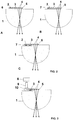
- FIG. 2 shows axial sections of various embodiments of the integrated lens antenna according to the present invention.
- the integrated lens antenna comprises a homogeneous dielectric lens 1, primary antenna elements 4 and transmission lines for connecting thereof (not shown), a switching network 3 adapted to apply electric power to at least one primary antenna element, and a transceiver 2.
- Switching network 3 and transceiver 2 are formed on semiconductor integrated circuits.
- Primary antenna elements 4 and transmission lines are formed on high frequency dielectric board 5 and integrated on a flat surface of homogeneous dielectric lens 1.
- a multilayer printed or ceramic board can be used as a high frequency dielectric board 5.
- FIG. 2 illustrates various relative arrangements of transceiver 2 and switching network 3 on dielectric board 5.
- dielectric board 5 has blind cavities for switching network 3 and transceiver 2 mounting.
- Switching network 3 and transceiver 2 are electrically connected to the transmission lines by means of wire bond connections 6.
- transceiver 2 and switching network 3 are electrically connected to dielectric board 5 by means of flip-chip connections 7.
- transceiver 2 and switching network 3 are electrically connected to dielectric board 5 by means of flip-chip connections 7 on the side of lens 1.
- lens 1 has special cut-outs for transceiver 2 and switching network 3.
- Such configuration can be used even in case of a one-layer dielectric board 5 made of high temperature co-fired ceramics, for example.
- such configuration requires minimizing leakage radiation from transceiver 2 and switching network 3 as well as the points of their connections to dielectric board 5 into the body of lens 1, for example by covering an inner surface of the cut-outs with metal.
- the antenna elements are located in between the lens and the PCB to provide the most effective lens feeding.
- FIG. 3 shows an axial section of the lens antenna according to the embodiment wherein a transceiver 8 is formed by means of waveguide elements and electrically connected to the board 5 by means of waveguide 9 and waveguide to microstrip transition 10.
- Switching network 3 can be arranged on dielectric board 5 according to one of the configurations illustrated in FIG. 2 .
- FIG. 4 illustrates an embodiment with separate signal receiving and transmitting functions.
- the present integrated lens antenna comprises two arrays of antenna elements 13 integrated on lens 1. One of the arrays is adapted to transmit a signal having a first linear polarization, and another array is adapted to receive a signal having a second linear polarization, orthogonal to the first linear polarization.
- the integrated lens antenna comprises two switching networks. Each switching network is adapted to independently control one of the arrays of primary antenna elements.
- each primary antenna element 13 is adapted to transmit a signal having a first linear polarization and to receive a signal having a second linear polarization, orthogonal to the first linear polarization.
- the integrated lens antenna comprises two switching networks. Each switching network is adapted to independently control the primary antenna elements while transmitting a signal having the first linear polarization and receiving a signal having the second linear polarization, respectively.
- the switching network comprises at least one 1 ⁇ N switch formed on the semiconductor integrated circuits, wherein N ⁇ 2.
- FIG. 5 illustrates example switching networks for 16 primary antenna elements, wherein FIG. 5a illustrates a case of using switches of 1 ⁇ 2 type, and Fig. 5b illustrates a case of using switches of 1 ⁇ 4 type. Each switch can be formed on a separate semiconductor integrated circuit.
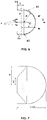
- FIG. 6 illustrates hemiellipsoidal and hemispherical shapes of dielectric lens 1 having a cylindrical extension.
- the length of the cylindrical extension can be set on the basis of the analysis of final characteristics of the antenna according to the present invention with a particular primary antenna element.
- the main requirement for the material of the dielectric lens according to the present invention is ability to provide a low level of dielectric losses.
- the lens weight is reduced by truncating a lens portion which does not positively contribute to the directivity of the lens antenna.
- FIG. 7 illustrates a corresponding hemispherical shape of the dielectric lens having a truncated cone extension. The weight reduction is important for large antennas used in radio relay stations.
- FIG. 8 illustrates a microstrip antenna configuration used as a primary antenna element in the lens antenna according to the present invention. According to the illustrated configuration, the electromagnetic coupling occurs through the slot aperture in the ground plane.
- a dual polarization microstrip antenna element is used as a primary antenna element.
- the dual polarization is achieved by means of two feed points through via holes 91 for direct signal inputting.
- Various dipoles, slot antennas etc. may be also used as planar primary antenna elements for integrated lens antennas.
- small dielectric permittivity antenna elements having the major portion of the radiation concentrated in one half-space, i.e. half-space on the side of the lens, are preferable.
- antenna elements include the above described microstrip antenna elements having different techniques for signal inputting, wherein the presence of a large ground plane ensures a radiation pattern concentrated in the half-space on the side of the lens.
- a radiation pattern having a beam deviation in a specific direction is formed.
- the narrow beam direction can be corrected by switching primary antenna elements 4 with the help of switching network 3.
- Primary antenna elements 4 having a small size can be configured so as to provide beam overlapping at an acceptable level, e.g. the level corresponding to a half radiation pattern beamwidth, while electronic beam steering.
- the low cost integrated lens antenna according to the present invention allows for electronic beam steering in a continuous angle sector while increasing radiation efficiency and reducing signal losses.
Landscapes
- Engineering & Computer Science (AREA)
- Computer Networks & Wireless Communication (AREA)
- Signal Processing (AREA)
- Variable-Direction Aerials And Aerial Arrays (AREA)
- Aerials With Secondary Devices (AREA)
Claims (15)
- Dispositif d'antenne à faisceau orientable électroniquement comprenant
une lentille diélectrique (1) ayant une surface sensiblement plate,
une carte diélectrique haute fréquence (5),
au moins deux éléments d'antenne primaire (4) et au moins deux lignes de transmission formés sur la carte diélectrique haute fréquence (5), et
un réseau de commutation (3) connecté électriquement aux au moins deux éléments d'antenne primaire (4) et aux au moins deux lignes de transmission et adapté pour appliquer une puissance électrique à au moins l'un des éléments d'antenne primaire (4) à travers au moins l'une des lignes de transmission,
dans lequel le réseau de commutation (3) est au moins un circuit intégré à semi-conducteur monté dans ou sur la carte diélectrique haute fréquence (5), et
la carte diélectrique haute fréquence (5) avec les au moins deux éléments d'antenne primaire (4) et les au moins deux lignes de transmission formés dessus est adjacente à la surface plate de la lentille diélectrique (1),
caractérisé en ce que les au moins deux éléments d'antenne (4) sont formés entre la carte diélectrique haute fréquence (5) et la lentille diélectrique (1). - Dispositif d'antenne selon la revendication 1, comprenant en outre un émetteur-récepteur (2) formé sur des circuits intégrés à semi-conducteur et connecté électriquement au réseau de commutation (3), dans lequel les circuits intégrés de l'émetteur-récepteur sont montés sur la carte diélectrique haute fréquence (5).
- Dispositif d'antenne selon la revendication 2, dans lequel l'émetteur-récepteur (2), le réseau de commutation (3), et au moins deux lignes de transmission sont positionnés sur le côté de la carte diélectrique (5) opposé à la lentille diélectrique (1).
- Dispositif d'antenne selon la revendication 2, dans lequel l'émetteur-récepteur (2) et le réseau de commutation (3) sont connectés électriquement l'un à l'autre et auxdits au moins deux éléments d'antenne primaire (4) au moyen d'une soudure de fils (6) ou de connexions par billes (7).
- Dispositif d'antenne selon la revendication 2, dans lequel l'émetteur-récepteur (2) et le réseau de commutation (3) sont montés dans des cavités borgnes formées dans la carte diélectrique haute fréquence (5).
- Dispositif d'antenne selon la revendication 1, dans lequel la carte diélectrique haute fréquence (5) est réalisée en céramique co-cuite haute température ou en céramique co-cuite basse température ou en une carte de circuit imprimé.
- Dispositif d'antenne selon la revendication 1, comprenant en outre un émetteur-récepteur (2) formé au moyen d'éléments de guide d'onde et connecté électriquement au moyen d'un guide d'onde (9) pour transiter en microruban (10) jusqu'au réseau de commutation (3) monté sur la carte diélectrique haute fréquence (5) .
- Dispositif d'antenne selon l'une quelconque des revendications 1 à 7, dans lequel le réseau de commutation (3) comprend au moins un commutateur 1 x N monté sur un circuit intégré à semi-conducteur, dans lequel N ≥ 2.
- Dispositif d'antenne selon l'une quelconque des revendications 1 à 8, dans lequel ledit dispositif d'antenne comprend en outre
un autre réseau de commutation (3) et
lesdits au moins deux éléments d'antenne primaire (4) comprennent deux ensembles d'éléments d'antenne primaire (4),
le premier ensemble étant adapté pour transmettre un signal ayant une première polarisation linéaire,
le second ensemble étant adapté pour recevoir un signal ayant une seconde polarisation linéaire orthogonale à la première polarisation linéaire, et
chaque réseau de commutation (3) étant adapté pour commander indépendamment l'un des deux ensembles d'éléments d'antenne primaire (4). - Dispositif d'antenne selon l'une quelconque des revendications 1 à 9, dans lequel ledit dispositif d'antenne comprend en outre
un autre réseau de commutation (3) et
chaque élément d'antenne primaire (4) est adapté pour transmettre un signal ayant une première polarisation linéaire et pour recevoir un signal ayant une seconde polarisation linéaire, orthogonale à la première polarisation linéaire,
chaque réseau de commutation (3) étant adapté pour commander indépendamment lesdits au moins deux éléments d'antenne primaire (4) tout en transmettant un signal ayant la première polarisation linéaire et en recevant un signal ayant la seconde polarisation linéaire, respectivement. - Dispositif d'antenne selon la revendication 10, dans lequel lesdits au moins deux éléments d'antenne primaire (4) sont au moins l'un d'éléments d'antenne microruban, d'éléments d'antenne dipôle et d'éléments d'antenne fendue.
- Dispositif d'antenne selon l'une quelconque des revendications 1 à 11, dans lequel une forme de lentille diélectrique (1) est choisie dans le groupe comprenant une forme hémiellipsoïdale avec une extension cylindrique, une forme hémisphérique avec une extension cylindrique, une forme hémiellipsoïdale avec une extension tronconique, et une forme d'un ellipsoïde tronqué avec un plan s'étendant perpendiculairement à un axe de l'ellipsoïde à proximité d'un foyer de l'ellipsoïde.
- Dispositif d'antenne selon l'une quelconque des revendications 1 à 12, dans lequel ledit dispositif d'antenne est adapté pour fournir une communication d'onde millimétrique point à point à haut débit et pour régler un faisceau dans le cas d'un réglage initial ou de légers changements d'orientation du dispositif d'antenne dus à des effets externes tels que le vent, des vibrations, une compression et/ou une extension de portions de la structure de support avec les changements de température, etc.
- Relais de faisceau hertzien pour des communications d'onde millimétrique point à point à haut débit, comprenant un dispositif d'antenne selon l'une quelconque des revendications 1 à 13.
- Procédé de communications d'onde millimétrique point à point à haut débit incluant les étapes de :fourniture d'un dispositif d'antenne à faisceau orientable électroniquement comprenant au moins deux éléments d'antenne primaire (4) et des lignes de transmission, selon l'une quelconque des revendications 1 à 13 ;application d'une puissance électrique à l'au moins un élément d'antenne primaire (4) du dispositif d'antenne pour former un schéma de rayonnement ayant un écart de faisceau dans une direction spécifique ;commutation de l'au moins un élément d'antenne primaire (4) par le réseau de commutation (3) lorsqu'il est nécessaire de régler la direction de faisceau en réponse à un changement d'orientation du dispositif d'antenne ; etréception et/ou transmission de signaux par le dispositif d'antenne.
Applications Claiming Priority (1)
| Application Number | Priority Date | Filing Date | Title |
|---|---|---|---|
| PCT/RU2011/000371 WO2012161612A1 (fr) | 2011-05-23 | 2011-05-23 | Dispositif d'antenne à faisceau orientable électroniquement |
Publications (2)
| Publication Number | Publication Date |
|---|---|
| EP2715869A1 EP2715869A1 (fr) | 2014-04-09 |
| EP2715869B1 true EP2715869B1 (fr) | 2018-04-18 |
Family
ID=45316031
Family Applications (1)
| Application Number | Title | Priority Date | Filing Date |
|---|---|---|---|
| EP11794262.3A Active EP2715869B1 (fr) | 2011-05-23 | 2011-05-23 | Dispositif d'antenne à faisceau orientable électroniquement |
Country Status (4)
| Country | Link |
|---|---|
| US (1) | US9590300B2 (fr) |
| EP (1) | EP2715869B1 (fr) |
| RU (1) | RU2586023C2 (fr) |
| WO (1) | WO2012161612A1 (fr) |
Families Citing this family (208)
| Publication number | Priority date | Publication date | Assignee | Title |
|---|---|---|---|---|
| WO2012161612A1 (fr) | 2011-05-23 | 2012-11-29 | Autonomous Non-Commercial Organization "Research Institute "Sitronics Labs"" | Dispositif d'antenne à faisceau orientable électroniquement |
| RU2585309C2 (ru) | 2011-10-20 | 2016-05-27 | Общество с ограниченной ответственностью "Радио Гигабит" | Система и способ радиорелейной связи с электронной подстройкой луча |
| RU2494506C1 (ru) * | 2012-07-10 | 2013-09-27 | Общество с ограниченной ответственностью "Радио Гигабит" | Линзовая антенна с электронным сканированием луча |
| US10009065B2 (en) | 2012-12-05 | 2018-06-26 | At&T Intellectual Property I, L.P. | Backhaul link for distributed antenna system |
| US9113347B2 (en) | 2012-12-05 | 2015-08-18 | At&T Intellectual Property I, Lp | Backhaul link for distributed antenna system |
| RU2530330C1 (ru) | 2013-03-22 | 2014-10-10 | Общество с ограниченной ответственностью "Радио Гигабит" | Станция радиорелейной связи со сканирующей антенной |
| US9999038B2 (en) | 2013-05-31 | 2018-06-12 | At&T Intellectual Property I, L.P. | Remote distributed antenna system |
| US9525524B2 (en) | 2013-05-31 | 2016-12-20 | At&T Intellectual Property I, L.P. | Remote distributed antenna system |
| US8897697B1 (en) | 2013-11-06 | 2014-11-25 | At&T Intellectual Property I, Lp | Millimeter-wave surface-wave communications |
| US9209902B2 (en) | 2013-12-10 | 2015-12-08 | At&T Intellectual Property I, L.P. | Quasi-optical coupler |
| US11647478B2 (en) * | 2014-01-22 | 2023-05-09 | Maxlinear, Inc. | Network discovery in an autoconfigured backhaul transceiver |
| WO2016023206A1 (fr) * | 2014-08-14 | 2016-02-18 | 华为技术有限公司 | Antenne à balayage de faisceau, système hyperfréquence et procédé d'alignement de faisceau |
| US9692101B2 (en) | 2014-08-26 | 2017-06-27 | At&T Intellectual Property I, L.P. | Guided wave couplers for coupling electromagnetic waves between a waveguide surface and a surface of a wire |
| US9768833B2 (en) | 2014-09-15 | 2017-09-19 | At&T Intellectual Property I, L.P. | Method and apparatus for sensing a condition in a transmission medium of electromagnetic waves |
| US10063280B2 (en) | 2014-09-17 | 2018-08-28 | At&T Intellectual Property I, L.P. | Monitoring and mitigating conditions in a communication network |
| US9628854B2 (en) | 2014-09-29 | 2017-04-18 | At&T Intellectual Property I, L.P. | Method and apparatus for distributing content in a communication network |
| US9615269B2 (en) | 2014-10-02 | 2017-04-04 | At&T Intellectual Property I, L.P. | Method and apparatus that provides fault tolerance in a communication network |
| US9685992B2 (en) | 2014-10-03 | 2017-06-20 | At&T Intellectual Property I, L.P. | Circuit panel network and methods thereof |
| US9503189B2 (en) | 2014-10-10 | 2016-11-22 | At&T Intellectual Property I, L.P. | Method and apparatus for arranging communication sessions in a communication system |
| US9973299B2 (en) | 2014-10-14 | 2018-05-15 | At&T Intellectual Property I, L.P. | Method and apparatus for adjusting a mode of communication in a communication network |
| US9762289B2 (en) | 2014-10-14 | 2017-09-12 | At&T Intellectual Property I, L.P. | Method and apparatus for transmitting or receiving signals in a transportation system |
| US9564947B2 (en) | 2014-10-21 | 2017-02-07 | At&T Intellectual Property I, L.P. | Guided-wave transmission device with diversity and methods for use therewith |
| US9520945B2 (en) | 2014-10-21 | 2016-12-13 | At&T Intellectual Property I, L.P. | Apparatus for providing communication services and methods thereof |
| US9577306B2 (en) | 2014-10-21 | 2017-02-21 | At&T Intellectual Property I, L.P. | Guided-wave transmission device and methods for use therewith |
| US9769020B2 (en) | 2014-10-21 | 2017-09-19 | At&T Intellectual Property I, L.P. | Method and apparatus for responding to events affecting communications in a communication network |
| US9653770B2 (en) | 2014-10-21 | 2017-05-16 | At&T Intellectual Property I, L.P. | Guided wave coupler, coupling module and methods for use therewith |
| US9627768B2 (en) | 2014-10-21 | 2017-04-18 | At&T Intellectual Property I, L.P. | Guided-wave transmission device with non-fundamental mode propagation and methods for use therewith |
| US9312919B1 (en) | 2014-10-21 | 2016-04-12 | At&T Intellectual Property I, Lp | Transmission device with impairment compensation and methods for use therewith |
| US9780834B2 (en) | 2014-10-21 | 2017-10-03 | At&T Intellectual Property I, L.P. | Method and apparatus for transmitting electromagnetic waves |
| US9680670B2 (en) | 2014-11-20 | 2017-06-13 | At&T Intellectual Property I, L.P. | Transmission device with channel equalization and control and methods for use therewith |
| US9954287B2 (en) | 2014-11-20 | 2018-04-24 | At&T Intellectual Property I, L.P. | Apparatus for converting wireless signals and electromagnetic waves and methods thereof |
| US9742462B2 (en) | 2014-12-04 | 2017-08-22 | At&T Intellectual Property I, L.P. | Transmission medium and communication interfaces and methods for use therewith |
| US9654173B2 (en) | 2014-11-20 | 2017-05-16 | At&T Intellectual Property I, L.P. | Apparatus for powering a communication device and methods thereof |
| US9997819B2 (en) | 2015-06-09 | 2018-06-12 | At&T Intellectual Property I, L.P. | Transmission medium and method for facilitating propagation of electromagnetic waves via a core |
| US9544006B2 (en) | 2014-11-20 | 2017-01-10 | At&T Intellectual Property I, L.P. | Transmission device with mode division multiplexing and methods for use therewith |
| US10340573B2 (en) | 2016-10-26 | 2019-07-02 | At&T Intellectual Property I, L.P. | Launcher with cylindrical coupling device and methods for use therewith |
| US10243784B2 (en) | 2014-11-20 | 2019-03-26 | At&T Intellectual Property I, L.P. | System for generating topology information and methods thereof |
| US10009067B2 (en) | 2014-12-04 | 2018-06-26 | At&T Intellectual Property I, L.P. | Method and apparatus for configuring a communication interface |
| US9461706B1 (en) | 2015-07-31 | 2016-10-04 | At&T Intellectual Property I, Lp | Method and apparatus for exchanging communication signals |
| US9800327B2 (en) | 2014-11-20 | 2017-10-24 | At&T Intellectual Property I, L.P. | Apparatus for controlling operations of a communication device and methods thereof |
| EP3048665B1 (fr) * | 2015-01-23 | 2022-04-27 | Alcatel Lucent | Noeud de réseau point à point et d'orientation de faisceau |
| US10144036B2 (en) | 2015-01-30 | 2018-12-04 | At&T Intellectual Property I, L.P. | Method and apparatus for mitigating interference affecting a propagation of electromagnetic waves guided by a transmission medium |
| US9876570B2 (en) | 2015-02-20 | 2018-01-23 | At&T Intellectual Property I, Lp | Guided-wave transmission device with non-fundamental mode propagation and methods for use therewith |
| US9749013B2 (en) | 2015-03-17 | 2017-08-29 | At&T Intellectual Property I, L.P. | Method and apparatus for reducing attenuation of electromagnetic waves guided by a transmission medium |
| US9705561B2 (en) | 2015-04-24 | 2017-07-11 | At&T Intellectual Property I, L.P. | Directional coupling device and methods for use therewith |
| US10224981B2 (en) | 2015-04-24 | 2019-03-05 | At&T Intellectual Property I, Lp | Passive electrical coupling device and methods for use therewith |
| US9793954B2 (en) | 2015-04-28 | 2017-10-17 | At&T Intellectual Property I, L.P. | Magnetic coupling device and methods for use therewith |
| US9948354B2 (en) | 2015-04-28 | 2018-04-17 | At&T Intellectual Property I, L.P. | Magnetic coupling device with reflective plate and methods for use therewith |
| US9871282B2 (en) | 2015-05-14 | 2018-01-16 | At&T Intellectual Property I, L.P. | At least one transmission medium having a dielectric surface that is covered at least in part by a second dielectric |
| US9490869B1 (en) | 2015-05-14 | 2016-11-08 | At&T Intellectual Property I, L.P. | Transmission medium having multiple cores and methods for use therewith |
| US9748626B2 (en) | 2015-05-14 | 2017-08-29 | At&T Intellectual Property I, L.P. | Plurality of cables having different cross-sectional shapes which are bundled together to form a transmission medium |
| US10650940B2 (en) | 2015-05-15 | 2020-05-12 | At&T Intellectual Property I, L.P. | Transmission medium having a conductive material and methods for use therewith |
| US10679767B2 (en) | 2015-05-15 | 2020-06-09 | At&T Intellectual Property I, L.P. | Transmission medium having a conductive material and methods for use therewith |
| US9917341B2 (en) | 2015-05-27 | 2018-03-13 | At&T Intellectual Property I, L.P. | Apparatus and method for launching electromagnetic waves and for modifying radial dimensions of the propagating electromagnetic waves |
| US10348391B2 (en) | 2015-06-03 | 2019-07-09 | At&T Intellectual Property I, L.P. | Client node device with frequency conversion and methods for use therewith |
| US10154493B2 (en) | 2015-06-03 | 2018-12-11 | At&T Intellectual Property I, L.P. | Network termination and methods for use therewith |
| US10812174B2 (en) | 2015-06-03 | 2020-10-20 | At&T Intellectual Property I, L.P. | Client node device and methods for use therewith |
| US10103801B2 (en) | 2015-06-03 | 2018-10-16 | At&T Intellectual Property I, L.P. | Host node device and methods for use therewith |
| US9866309B2 (en) | 2015-06-03 | 2018-01-09 | At&T Intellectual Property I, Lp | Host node device and methods for use therewith |
| US9912381B2 (en) | 2015-06-03 | 2018-03-06 | At&T Intellectual Property I, Lp | Network termination and methods for use therewith |
| US9913139B2 (en) | 2015-06-09 | 2018-03-06 | At&T Intellectual Property I, L.P. | Signal fingerprinting for authentication of communicating devices |
| US9608692B2 (en) | 2015-06-11 | 2017-03-28 | At&T Intellectual Property I, L.P. | Repeater and methods for use therewith |
| US10142086B2 (en) | 2015-06-11 | 2018-11-27 | At&T Intellectual Property I, L.P. | Repeater and methods for use therewith |
| US9820146B2 (en) | 2015-06-12 | 2017-11-14 | At&T Intellectual Property I, L.P. | Method and apparatus for authentication and identity management of communicating devices |
| US9667317B2 (en) | 2015-06-15 | 2017-05-30 | At&T Intellectual Property I, L.P. | Method and apparatus for providing security using network traffic adjustments |
| US9509415B1 (en) | 2015-06-25 | 2016-11-29 | At&T Intellectual Property I, L.P. | Methods and apparatus for inducing a fundamental wave mode on a transmission medium |
| US9865911B2 (en) | 2015-06-25 | 2018-01-09 | At&T Intellectual Property I, L.P. | Waveguide system for slot radiating first electromagnetic waves that are combined into a non-fundamental wave mode second electromagnetic wave on a transmission medium |
| US9640850B2 (en) | 2015-06-25 | 2017-05-02 | At&T Intellectual Property I, L.P. | Methods and apparatus for inducing a non-fundamental wave mode on a transmission medium |
| US10033108B2 (en) | 2015-07-14 | 2018-07-24 | At&T Intellectual Property I, L.P. | Apparatus and methods for generating an electromagnetic wave having a wave mode that mitigates interference |
| US9847566B2 (en) | 2015-07-14 | 2017-12-19 | At&T Intellectual Property I, L.P. | Method and apparatus for adjusting a field of a signal to mitigate interference |
| US10320586B2 (en) | 2015-07-14 | 2019-06-11 | At&T Intellectual Property I, L.P. | Apparatus and methods for generating non-interfering electromagnetic waves on an insulated transmission medium |
| US10148016B2 (en) | 2015-07-14 | 2018-12-04 | At&T Intellectual Property I, L.P. | Apparatus and methods for communicating utilizing an antenna array |
| US10044409B2 (en) | 2015-07-14 | 2018-08-07 | At&T Intellectual Property I, L.P. | Transmission medium and methods for use therewith |
| US9836957B2 (en) | 2015-07-14 | 2017-12-05 | At&T Intellectual Property I, L.P. | Method and apparatus for communicating with premises equipment |
| US9882257B2 (en) | 2015-07-14 | 2018-01-30 | At&T Intellectual Property I, L.P. | Method and apparatus for launching a wave mode that mitigates interference |
| US9722318B2 (en) | 2015-07-14 | 2017-08-01 | At&T Intellectual Property I, L.P. | Method and apparatus for coupling an antenna to a device |
| US9628116B2 (en) | 2015-07-14 | 2017-04-18 | At&T Intellectual Property I, L.P. | Apparatus and methods for transmitting wireless signals |
| US10341142B2 (en) | 2015-07-14 | 2019-07-02 | At&T Intellectual Property I, L.P. | Apparatus and methods for generating non-interfering electromagnetic waves on an uninsulated conductor |
| US10170840B2 (en) | 2015-07-14 | 2019-01-01 | At&T Intellectual Property I, L.P. | Apparatus and methods for sending or receiving electromagnetic signals |
| US10205655B2 (en) | 2015-07-14 | 2019-02-12 | At&T Intellectual Property I, L.P. | Apparatus and methods for communicating utilizing an antenna array and multiple communication paths |
| US10033107B2 (en) | 2015-07-14 | 2018-07-24 | At&T Intellectual Property I, L.P. | Method and apparatus for coupling an antenna to a device |
| US9853342B2 (en) | 2015-07-14 | 2017-12-26 | At&T Intellectual Property I, L.P. | Dielectric transmission medium connector and methods for use therewith |
| US10090606B2 (en) | 2015-07-15 | 2018-10-02 | At&T Intellectual Property I, L.P. | Antenna system with dielectric array and methods for use therewith |
| US9793951B2 (en) | 2015-07-15 | 2017-10-17 | At&T Intellectual Property I, L.P. | Method and apparatus for launching a wave mode that mitigates interference |
| US9608740B2 (en) | 2015-07-15 | 2017-03-28 | At&T Intellectual Property I, L.P. | Method and apparatus for launching a wave mode that mitigates interference |
| US10784670B2 (en) | 2015-07-23 | 2020-09-22 | At&T Intellectual Property I, L.P. | Antenna support for aligning an antenna |
| US9912027B2 (en) | 2015-07-23 | 2018-03-06 | At&T Intellectual Property I, L.P. | Method and apparatus for exchanging communication signals |
| US9749053B2 (en) | 2015-07-23 | 2017-08-29 | At&T Intellectual Property I, L.P. | Node device, repeater and methods for use therewith |
| US9948333B2 (en) | 2015-07-23 | 2018-04-17 | At&T Intellectual Property I, L.P. | Method and apparatus for wireless communications to mitigate interference |
| US9871283B2 (en) | 2015-07-23 | 2018-01-16 | At&T Intellectual Property I, Lp | Transmission medium having a dielectric core comprised of plural members connected by a ball and socket configuration |
| US9735833B2 (en) | 2015-07-31 | 2017-08-15 | At&T Intellectual Property I, L.P. | Method and apparatus for communications management in a neighborhood network |
| US9967173B2 (en) | 2015-07-31 | 2018-05-08 | At&T Intellectual Property I, L.P. | Method and apparatus for authentication and identity management of communicating devices |
| US10020587B2 (en) | 2015-07-31 | 2018-07-10 | At&T Intellectual Property I, L.P. | Radial antenna and methods for use therewith |
| US11050157B2 (en) * | 2015-08-05 | 2021-06-29 | Matsing, Inc. | Antenna lens array for tracking multiple devices |
| US9904535B2 (en) | 2015-09-14 | 2018-02-27 | At&T Intellectual Property I, L.P. | Method and apparatus for distributing software |
| US10079661B2 (en) | 2015-09-16 | 2018-09-18 | At&T Intellectual Property I, L.P. | Method and apparatus for use with a radio distributed antenna system having a clock reference |
| US9705571B2 (en) | 2015-09-16 | 2017-07-11 | At&T Intellectual Property I, L.P. | Method and apparatus for use with a radio distributed antenna system |
| US10009063B2 (en) | 2015-09-16 | 2018-06-26 | At&T Intellectual Property I, L.P. | Method and apparatus for use with a radio distributed antenna system having an out-of-band reference signal |
| US10136434B2 (en) | 2015-09-16 | 2018-11-20 | At&T Intellectual Property I, L.P. | Method and apparatus for use with a radio distributed antenna system having an ultra-wideband control channel |
| US10051629B2 (en) | 2015-09-16 | 2018-08-14 | At&T Intellectual Property I, L.P. | Method and apparatus for use with a radio distributed antenna system having an in-band reference signal |
| US10009901B2 (en) | 2015-09-16 | 2018-06-26 | At&T Intellectual Property I, L.P. | Method, apparatus, and computer-readable storage medium for managing utilization of wireless resources between base stations |
| US9769128B2 (en) | 2015-09-28 | 2017-09-19 | At&T Intellectual Property I, L.P. | Method and apparatus for encryption of communications over a network |
| US9729197B2 (en) | 2015-10-01 | 2017-08-08 | At&T Intellectual Property I, L.P. | Method and apparatus for communicating network management traffic over a network |
| US9882277B2 (en) | 2015-10-02 | 2018-01-30 | At&T Intellectual Property I, Lp | Communication device and antenna assembly with actuated gimbal mount |
| US10074890B2 (en) | 2015-10-02 | 2018-09-11 | At&T Intellectual Property I, L.P. | Communication device and antenna with integrated light assembly |
| US9876264B2 (en) | 2015-10-02 | 2018-01-23 | At&T Intellectual Property I, Lp | Communication system, guided wave switch and methods for use therewith |
| US10665942B2 (en) | 2015-10-16 | 2020-05-26 | At&T Intellectual Property I, L.P. | Method and apparatus for adjusting wireless communications |
| US10355367B2 (en) | 2015-10-16 | 2019-07-16 | At&T Intellectual Property I, L.P. | Antenna structure for exchanging wireless signals |
| US10051483B2 (en) | 2015-10-16 | 2018-08-14 | At&T Intellectual Property I, L.P. | Method and apparatus for directing wireless signals |
| RU2649871C2 (ru) * | 2016-06-24 | 2018-04-05 | Общество с ограниченной ответственностью "Радио Гигабит" | Устройство беспроводной связи с частотно-поляризационной развязкой между передающим и приемным каналами |
| US9912419B1 (en) | 2016-08-24 | 2018-03-06 | At&T Intellectual Property I, L.P. | Method and apparatus for managing a fault in a distributed antenna system |
| US9860075B1 (en) | 2016-08-26 | 2018-01-02 | At&T Intellectual Property I, L.P. | Method and communication node for broadband distribution |
| US10291311B2 (en) | 2016-09-09 | 2019-05-14 | At&T Intellectual Property I, L.P. | Method and apparatus for mitigating a fault in a distributed antenna system |
| US11032819B2 (en) | 2016-09-15 | 2021-06-08 | At&T Intellectual Property I, L.P. | Method and apparatus for use with a radio distributed antenna system having a control channel reference signal |
| US10135147B2 (en) | 2016-10-18 | 2018-11-20 | At&T Intellectual Property I, L.P. | Apparatus and methods for launching guided waves via an antenna |
| US10340600B2 (en) | 2016-10-18 | 2019-07-02 | At&T Intellectual Property I, L.P. | Apparatus and methods for launching guided waves via plural waveguide systems |
| US10135146B2 (en) | 2016-10-18 | 2018-11-20 | At&T Intellectual Property I, L.P. | Apparatus and methods for launching guided waves via circuits |
| US10811767B2 (en) | 2016-10-21 | 2020-10-20 | At&T Intellectual Property I, L.P. | System and dielectric antenna with convex dielectric radome |
| US9876605B1 (en) | 2016-10-21 | 2018-01-23 | At&T Intellectual Property I, L.P. | Launcher and coupling system to support desired guided wave mode |
| US10374316B2 (en) | 2016-10-21 | 2019-08-06 | At&T Intellectual Property I, L.P. | System and dielectric antenna with non-uniform dielectric |
| US9991580B2 (en) | 2016-10-21 | 2018-06-05 | At&T Intellectual Property I, L.P. | Launcher and coupling system for guided wave mode cancellation |
| US10312567B2 (en) | 2016-10-26 | 2019-06-04 | At&T Intellectual Property I, L.P. | Launcher with planar strip antenna and methods for use therewith |
| US10498044B2 (en) | 2016-11-03 | 2019-12-03 | At&T Intellectual Property I, L.P. | Apparatus for configuring a surface of an antenna |
| US10225025B2 (en) | 2016-11-03 | 2019-03-05 | At&T Intellectual Property I, L.P. | Method and apparatus for detecting a fault in a communication system |
| US10224634B2 (en) | 2016-11-03 | 2019-03-05 | At&T Intellectual Property I, L.P. | Methods and apparatus for adjusting an operational characteristic of an antenna |
| US10291334B2 (en) | 2016-11-03 | 2019-05-14 | At&T Intellectual Property I, L.P. | System for detecting a fault in a communication system |
| US10178445B2 (en) | 2016-11-23 | 2019-01-08 | At&T Intellectual Property I, L.P. | Methods, devices, and systems for load balancing between a plurality of waveguides |
| US10090594B2 (en) | 2016-11-23 | 2018-10-02 | At&T Intellectual Property I, L.P. | Antenna system having structural configurations for assembly |
| US10535928B2 (en) | 2016-11-23 | 2020-01-14 | At&T Intellectual Property I, L.P. | Antenna system and methods for use therewith |
| US10340601B2 (en) | 2016-11-23 | 2019-07-02 | At&T Intellectual Property I, L.P. | Multi-antenna system and methods for use therewith |
| US10340603B2 (en) | 2016-11-23 | 2019-07-02 | At&T Intellectual Property I, L.P. | Antenna system having shielded structural configurations for assembly |
| US10305190B2 (en) | 2016-12-01 | 2019-05-28 | At&T Intellectual Property I, L.P. | Reflecting dielectric antenna system and methods for use therewith |
| US10361489B2 (en) | 2016-12-01 | 2019-07-23 | At&T Intellectual Property I, L.P. | Dielectric dish antenna system and methods for use therewith |
| US10694379B2 (en) | 2016-12-06 | 2020-06-23 | At&T Intellectual Property I, L.P. | Waveguide system with device-based authentication and methods for use therewith |
| US10819035B2 (en) | 2016-12-06 | 2020-10-27 | At&T Intellectual Property I, L.P. | Launcher with helical antenna and methods for use therewith |
| US10439675B2 (en) | 2016-12-06 | 2019-10-08 | At&T Intellectual Property I, L.P. | Method and apparatus for repeating guided wave communication signals |
| US10135145B2 (en) | 2016-12-06 | 2018-11-20 | At&T Intellectual Property I, L.P. | Apparatus and methods for generating an electromagnetic wave along a transmission medium |
| US9927517B1 (en) | 2016-12-06 | 2018-03-27 | At&T Intellectual Property I, L.P. | Apparatus and methods for sensing rainfall |
| US10382976B2 (en) | 2016-12-06 | 2019-08-13 | At&T Intellectual Property I, L.P. | Method and apparatus for managing wireless communications based on communication paths and network device positions |
| US10727599B2 (en) | 2016-12-06 | 2020-07-28 | At&T Intellectual Property I, L.P. | Launcher with slot antenna and methods for use therewith |
| US10637149B2 (en) | 2016-12-06 | 2020-04-28 | At&T Intellectual Property I, L.P. | Injection molded dielectric antenna and methods for use therewith |
| US10020844B2 (en) | 2016-12-06 | 2018-07-10 | T&T Intellectual Property I, L.P. | Method and apparatus for broadcast communication via guided waves |
| US10755542B2 (en) | 2016-12-06 | 2020-08-25 | At&T Intellectual Property I, L.P. | Method and apparatus for surveillance via guided wave communication |
| US10326494B2 (en) | 2016-12-06 | 2019-06-18 | At&T Intellectual Property I, L.P. | Apparatus for measurement de-embedding and methods for use therewith |
| US10446936B2 (en) | 2016-12-07 | 2019-10-15 | At&T Intellectual Property I, L.P. | Multi-feed dielectric antenna system and methods for use therewith |
| US9893795B1 (en) | 2016-12-07 | 2018-02-13 | At&T Intellectual Property I, Lp | Method and repeater for broadband distribution |
| US10139820B2 (en) | 2016-12-07 | 2018-11-27 | At&T Intellectual Property I, L.P. | Method and apparatus for deploying equipment of a communication system |
| US10243270B2 (en) | 2016-12-07 | 2019-03-26 | At&T Intellectual Property I, L.P. | Beam adaptive multi-feed dielectric antenna system and methods for use therewith |
| US10547348B2 (en) | 2016-12-07 | 2020-01-28 | At&T Intellectual Property I, L.P. | Method and apparatus for switching transmission mediums in a communication system |
| US10389029B2 (en) | 2016-12-07 | 2019-08-20 | At&T Intellectual Property I, L.P. | Multi-feed dielectric antenna system with core selection and methods for use therewith |
| US10027397B2 (en) | 2016-12-07 | 2018-07-17 | At&T Intellectual Property I, L.P. | Distributed antenna system and methods for use therewith |
| US10168695B2 (en) | 2016-12-07 | 2019-01-01 | At&T Intellectual Property I, L.P. | Method and apparatus for controlling an unmanned aircraft |
| US10359749B2 (en) | 2016-12-07 | 2019-07-23 | At&T Intellectual Property I, L.P. | Method and apparatus for utilities management via guided wave communication |
| US10103422B2 (en) | 2016-12-08 | 2018-10-16 | At&T Intellectual Property I, L.P. | Method and apparatus for mounting network devices |
| US10411356B2 (en) | 2016-12-08 | 2019-09-10 | At&T Intellectual Property I, L.P. | Apparatus and methods for selectively targeting communication devices with an antenna array |
| US9998870B1 (en) | 2016-12-08 | 2018-06-12 | At&T Intellectual Property I, L.P. | Method and apparatus for proximity sensing |
| US10916969B2 (en) | 2016-12-08 | 2021-02-09 | At&T Intellectual Property I, L.P. | Method and apparatus for providing power using an inductive coupling |
| US10530505B2 (en) | 2016-12-08 | 2020-01-07 | At&T Intellectual Property I, L.P. | Apparatus and methods for launching electromagnetic waves along a transmission medium |
| US10326689B2 (en) | 2016-12-08 | 2019-06-18 | At&T Intellectual Property I, L.P. | Method and system for providing alternative communication paths |
| US9911020B1 (en) | 2016-12-08 | 2018-03-06 | At&T Intellectual Property I, L.P. | Method and apparatus for tracking via a radio frequency identification device |
| US10389037B2 (en) | 2016-12-08 | 2019-08-20 | At&T Intellectual Property I, L.P. | Apparatus and methods for selecting sections of an antenna array and use therewith |
| US10777873B2 (en) | 2016-12-08 | 2020-09-15 | At&T Intellectual Property I, L.P. | Method and apparatus for mounting network devices |
| US10601494B2 (en) | 2016-12-08 | 2020-03-24 | At&T Intellectual Property I, L.P. | Dual-band communication device and method for use therewith |
| US10069535B2 (en) | 2016-12-08 | 2018-09-04 | At&T Intellectual Property I, L.P. | Apparatus and methods for launching electromagnetic waves having a certain electric field structure |
| US10938108B2 (en) | 2016-12-08 | 2021-03-02 | At&T Intellectual Property I, L.P. | Frequency selective multi-feed dielectric antenna system and methods for use therewith |
| US10264586B2 (en) | 2016-12-09 | 2019-04-16 | At&T Mobility Ii Llc | Cloud-based packet controller and methods for use therewith |
| US9838896B1 (en) | 2016-12-09 | 2017-12-05 | At&T Intellectual Property I, L.P. | Method and apparatus for assessing network coverage |
| US10340983B2 (en) | 2016-12-09 | 2019-07-02 | At&T Intellectual Property I, L.P. | Method and apparatus for surveying remote sites via guided wave communications |
| WO2018115372A1 (fr) * | 2016-12-23 | 2018-06-28 | Iee International Electronics & Engineering S.A. | Dispositif d'imagerie par ondes radar 3d à haute résolution |
| LU100259B1 (en) * | 2017-05-22 | 2019-01-04 | Iee Sa | High-Resolution 3D Radar Wave Imaging Device |
| US9973940B1 (en) | 2017-02-27 | 2018-05-15 | At&T Intellectual Property I, L.P. | Apparatus and methods for dynamic impedance matching of a guided wave launcher |
| US10298293B2 (en) | 2017-03-13 | 2019-05-21 | At&T Intellectual Property I, L.P. | Apparatus of communication utilizing wireless network devices |
| US10116051B2 (en) * | 2017-03-17 | 2018-10-30 | Isotropic Systems Ltd. | Lens antenna system |
| WO2018200567A1 (fr) * | 2017-04-24 | 2018-11-01 | Cohere Technologies | Conceptions et fonctionnement d'antenne multifaisceau |
| RU2660385C1 (ru) * | 2017-07-24 | 2018-07-06 | Общество с ограниченной ответственностью "Радио Модуль НН" | Сканирующая линзовая антенна |
| EP3769429B1 (fr) | 2018-03-19 | 2024-11-06 | Pivotal Commware, Inc. | Communication de signaux sans fil à travers des barrières physiques |
| CN108594171B (zh) * | 2018-04-28 | 2021-06-22 | 纳恩博(北京)科技有限公司 | 定位通信设备、定位方法及计算机存储介质 |
| RU2680429C1 (ru) | 2018-05-21 | 2019-02-21 | Самсунг Электроникс Ко., Лтд. | Оптически-управляемый переключатель миллиметрового диапазона и основанные на нем устройства |
| US10862545B2 (en) | 2018-07-30 | 2020-12-08 | Pivotal Commware, Inc. | Distributed antenna networks for wireless communication by wireless devices |
| US11552405B1 (en) * | 2018-09-21 | 2023-01-10 | Apple Inc. | Lens structure |
| EP3667813B1 (fr) * | 2018-12-10 | 2023-11-29 | indie Semiconductor FFO GmbH | Capteur radar avec antenne intégrée et lentille de focalisation |
| US10522897B1 (en) | 2019-02-05 | 2019-12-31 | Pivotal Commware, Inc. | Thermal compensation for a holographic beam forming antenna |
| US10468767B1 (en) | 2019-02-20 | 2019-11-05 | Pivotal Commware, Inc. | Switchable patch antenna |
| US10833415B2 (en) | 2019-04-11 | 2020-11-10 | The Boeing Company | Radio frequency circuit board with microstrip-to-waveguide transition |
| US10826196B1 (en) | 2019-04-11 | 2020-11-03 | The Boeing Company | Dielectric lens antenna |
| EP3758148A1 (fr) * | 2019-06-25 | 2020-12-30 | Nokia Solutions and Networks Oy | Antenne à directivité contrôlée |
| US10734736B1 (en) | 2020-01-03 | 2020-08-04 | Pivotal Commware, Inc. | Dual polarization patch antenna system |
| EP4111531A1 (fr) | 2020-02-25 | 2023-01-04 | All.Space Networks Limited | Prisme permettant de repointer un faisceau principal d'antenne à réflecteur |
| US11069975B1 (en) | 2020-04-13 | 2021-07-20 | Pivotal Commware, Inc. | Aimable beam antenna system |
| US11177548B1 (en) | 2020-05-04 | 2021-11-16 | The Boeing Company | Electromagnetic wave concentration |
| US12300890B2 (en) | 2020-05-19 | 2025-05-13 | Apothym Technologies Group, Llc | High-gain, hemi-spherical coverage, multi-sided flattened Luneburg lens antenna |
| JP2023527384A (ja) | 2020-05-27 | 2023-06-28 | ピヴォタル コムウェア インコーポレイテッド | 5gワイヤレスネットワーク用rf信号リピータデバイスの管理方法 |
| WO2022020844A1 (fr) * | 2020-07-21 | 2022-01-27 | Starry, Inc. | Nœud d'agrégation haute fréquence à lentilles permutables |
| US11026055B1 (en) | 2020-08-03 | 2021-06-01 | Pivotal Commware, Inc. | Wireless communication network management for user devices based on real time mapping |
| WO2022056024A1 (fr) | 2020-09-08 | 2022-03-17 | Pivotal Commware, Inc. | Installation et activation de dispositifs de communication rf pour réseaux sans fil |
| US12218426B2 (en) * | 2020-12-10 | 2025-02-04 | Intel Corporation | Low-profile single-chain beam-steerable MMW lens antenna |
| CN112563756B (zh) * | 2020-12-11 | 2026-03-24 | 福州盛博电子有限公司 | 一种高隔离度初级透镜天线系统和毫米波雷达传感器 |
| CA3208262A1 (fr) | 2021-01-15 | 2022-07-21 | Pivotal Commware, Inc. | Installation de repeteurs pour un reseau de communication a ondes millimetriques |
| AU2022212950A1 (en) | 2021-01-26 | 2023-09-07 | Pivotal Commware, Inc. | Smart repeater systems |
| US12126093B2 (en) * | 2021-02-01 | 2024-10-22 | The Regents Of The University Of California | Reconfigurable radiator array source for lens-coupled continuous, wide-angle, and directive beam steering |
| US11451287B1 (en) | 2021-03-16 | 2022-09-20 | Pivotal Commware, Inc. | Multipath filtering for wireless RF signals |
| US11929822B2 (en) | 2021-07-07 | 2024-03-12 | Pivotal Commware, Inc. | Multipath repeater systems |
| WO2023076405A1 (fr) | 2021-10-26 | 2023-05-04 | Pivotal Commware, Inc. | Structures d'absorption rf |
| WO2023205182A1 (fr) | 2022-04-18 | 2023-10-26 | Pivotal Commware, Inc. | Répéteurs duplex à répartition dans le temps avec récupération de synchronisation de système mondial de navigation par satellite |
| US11824271B1 (en) * | 2022-05-06 | 2023-11-21 | Qualcomm Incorporated | Transmit and receive antenna array configuration for radio frequency beamforming |
| US12308520B2 (en) * | 2022-05-06 | 2025-05-20 | Qualcomm Incorporated | Radio frequency beamforming device with cylindrical lens |
| US12300886B2 (en) * | 2022-08-10 | 2025-05-13 | Qualcomm Incorporated | Radio frequency beamforming device with cylindrical lenses |
| EP4621993A1 (fr) * | 2024-03-19 | 2025-09-24 | Nxp B.V. | Radar à antennes réseau de balayage à lentille diélectrique |
Family Cites Families (48)
| Publication number | Priority date | Publication date | Assignee | Title |
|---|---|---|---|---|
| US4574287A (en) * | 1983-03-04 | 1986-03-04 | The United States Of America As Represented By The Secretary Of The Navy | Fixed aperture, rotating feed, beam scanning antenna system |
| FR2581798B1 (fr) | 1985-05-10 | 1988-02-26 | Alcatel Thomson Faisceaux | Procede de pointage azimutal des antennes d'une liaison tropospherique |
| GB2252452B (en) * | 1985-09-05 | 1992-12-16 | Plessey Co Plc | Improvements in or relating to hybrid structures |
| FR2705169A1 (fr) | 1986-03-14 | 1994-11-18 | Thomson Csf | Antenne réseau bidimensionnel, à modules émetteurs-récepteurs répartis sur la surface de l'antenne, et à balayage électronique. |
| CA2027456C (fr) | 1989-11-08 | 1995-09-26 | Timothy A. Murphy | Reseau ameliore de mise en forme de faisceau pour systeme de communication par satellite |
| US5706017A (en) | 1993-04-21 | 1998-01-06 | California Institute Of Technology | Hybrid antenna including a dielectric lens and planar feed |
| US5486832A (en) | 1994-07-01 | 1996-01-23 | Hughes Missile Systems Company | RF sensor and radar for automotive speed and collision avoidance applications |
| US5481268A (en) | 1994-07-20 | 1996-01-02 | Rockwell International Corporation | Doppler radar system for automotive vehicles |
| FR2739974B1 (fr) | 1995-10-17 | 1998-01-09 | Dassault Electronique | Lentille electromagnetique de type circuit imprime a substrat suspendu |
| JPH1093321A (ja) * | 1996-09-18 | 1998-04-10 | Honda Motor Co Ltd | アンテナ装置 |
| DE19834577B4 (de) | 1998-07-31 | 2011-12-29 | Delphi Technologies, Inc. | Antennensystem |
| US6590544B1 (en) | 1998-09-01 | 2003-07-08 | Qualcomm, Inc. | Dielectric lens assembly for a feed antenna |
| RU2177662C1 (ru) * | 2000-11-17 | 2001-12-27 | Общество ограниченной ответственности НПФ "АЭРОФАР" | Двухдиапазонная антенная система с электронным управлением лучом |
| FI20010079A7 (fi) | 2001-01-12 | 2002-07-13 | Nokia Corp | Paikannusmenetelmä ja radiojärjestelmä |
| US20030022694A1 (en) | 2001-05-02 | 2003-01-30 | Randall Olsen | Communication system with multi-beam communication antenna |
| US6587699B2 (en) | 2001-05-02 | 2003-07-01 | Trex Enterprises Corporation | Narrow beamwidth communication link with alignment camera |
| US8090411B2 (en) | 2001-05-02 | 2012-01-03 | Trex Enterprises Corp | Wireless millimeter wave communication system |
| RU2291527C2 (ru) | 2001-09-28 | 2007-01-10 | ДжСАТ КОРПОРЕЙШН | Линзовое антенное устройство (варианты) и координатная карта для линзового антенного устройства (варианты) |
| SE0200792D0 (sv) | 2002-03-18 | 2002-03-18 | Saab Marine Electronics | Hornantenn |
| RU2236073C2 (ru) * | 2002-09-11 | 2004-09-10 | 16 Центральный научно-исследовательский испытательный институт Министерства обороны Российской Федерации | Тороидальная линзовая антенна с электронным сканированием в двух плоскостях |
| JP3858873B2 (ja) | 2002-12-02 | 2006-12-20 | 株式会社村田製作所 | アンテナ装置、無線装置およびレーダ |
| US6822615B2 (en) * | 2003-02-25 | 2004-11-23 | Raytheon Company | Wideband 2-D electronically scanned array with compact CTS feed and MEMS phase shifters |
| US6992621B2 (en) | 2003-03-07 | 2006-01-31 | Vivato, Inc. | Wireless communication and beam forming with passive beamformers |
| TWI289412B (en) | 2003-05-16 | 2007-11-01 | Interdigital Tech Corp | Coordination of backhaul beam forming in wireless communication systems |
| GB2415863A (en) * | 2004-07-01 | 2006-01-04 | British Sky Broadcasting Ltd | Wireless network system and devices with redundancy between orthogonally polarised beams |
| US6992622B1 (en) | 2004-10-15 | 2006-01-31 | Interdigital Technology Corporation | Wireless communication method and antenna system for determining direction of arrival information to form a three-dimensional beam used by a transceiver |
| US7687417B2 (en) * | 2005-11-16 | 2010-03-30 | E.I. Du Pont De Nemours And Company | Lead free glass(es), thick film paste(s), tape composition(s) and low temperature cofired ceramic devices made therefrom |
| WO2007136289A1 (fr) | 2006-05-23 | 2007-11-29 | Intel Corporation | Systèmes d'antennes à réseau de puces et de lentilles à ondes millimétriques pour réseaux sans fil |
| US7667665B1 (en) | 2006-11-01 | 2010-02-23 | Hrl Laboratories, Llc | Dual frequency aperture antenna |
| US7642961B1 (en) | 2006-12-19 | 2010-01-05 | Sprint Communications Company L.P. | Remote control antenna positioning system |
| US7683844B2 (en) | 2007-05-16 | 2010-03-23 | Intel Corporation | Mm-wave scanning antenna |
| RU2349007C1 (ru) * | 2007-06-04 | 2009-03-10 | Открытое акционерное общество "Научно-исследовательский институт приборостроения им. В.В. Тихомирова" | Двухдиапазонная антенная система с электронным управлением лучом |
| RU68191U1 (ru) | 2007-06-22 | 2007-11-10 | Федеральное государственное унитарное предприятие "Российский научно-исследовательский институт космического приборостроения" | Антенное устройство базовой станции беспроводной мобильной связи |
| US7844217B2 (en) | 2007-10-01 | 2010-11-30 | Provigent Ltd. | Point-to-multipoint communication terminal having a single RF chain |
| GB2459131A (en) | 2008-04-11 | 2009-10-14 | Vodafone Group Services Ltd | Locating nodes of a telecommunications system |
| US9036599B2 (en) | 2008-05-11 | 2015-05-19 | Qualcomm Incorporated | Systems and methods for multimode wireless communication handoff |
| US8411638B2 (en) | 2008-06-23 | 2013-04-02 | Qualcomm Incorporated | Methods and systems for background scanning in OFDMA mobile stations |
| US7834803B2 (en) | 2008-09-03 | 2010-11-16 | Lockheed Martin Corporation | Electronically steered, dual-polarized, dual-plane, monopulse antenna feed |
| US7688263B1 (en) | 2008-12-07 | 2010-03-30 | Roger Dale Oxley | Volumetric direction-finding system using a Luneberg Lens |
| US8487810B2 (en) | 2009-09-16 | 2013-07-16 | Broadcom Corporation | Integrated and configurable radar system |
| US8576132B2 (en) | 2009-10-22 | 2013-11-05 | Lockheed Martin Corporation | Metamaterial lens feed for multiple beam antennas |
| US10244579B2 (en) * | 2010-01-28 | 2019-03-26 | Samsung Electronics Co., Ltd. | Techniques for millimeter wave mobile communication |
| JP5654785B2 (ja) | 2010-06-28 | 2015-01-14 | 日鉄住金ファインテック株式会社 | 回転駆動装置および電波レンズアンテナ装置 |
| US9742077B2 (en) * | 2011-03-15 | 2017-08-22 | Intel Corporation | Mm-wave phased array antenna with beam tilting radiation pattern |
| WO2012161612A1 (fr) | 2011-05-23 | 2012-11-29 | Autonomous Non-Commercial Organization "Research Institute "Sitronics Labs"" | Dispositif d'antenne à faisceau orientable électroniquement |
| RU2585309C2 (ru) | 2011-10-20 | 2016-05-27 | Общество с ограниченной ответственностью "Радио Гигабит" | Система и способ радиорелейной связи с электронной подстройкой луча |
| RU2494506C1 (ru) | 2012-07-10 | 2013-09-27 | Общество с ограниченной ответственностью "Радио Гигабит" | Линзовая антенна с электронным сканированием луча |
| RU2530330C1 (ru) | 2013-03-22 | 2014-10-10 | Общество с ограниченной ответственностью "Радио Гигабит" | Станция радиорелейной связи со сканирующей антенной |
-
2011
- 2011-05-23 WO PCT/RU2011/000371 patent/WO2012161612A1/fr not_active Ceased
- 2011-05-23 EP EP11794262.3A patent/EP2715869B1/fr active Active
- 2011-05-23 RU RU2013156505/08A patent/RU2586023C2/ru active
-
2013
- 2013-11-25 US US14/088,875 patent/US9590300B2/en active Active
Non-Patent Citations (1)
| Title |
|---|
| None * |
Also Published As
| Publication number | Publication date |
|---|---|
| EP2715869A1 (fr) | 2014-04-09 |
| RU2013156505A (ru) | 2015-06-27 |
| US9590300B2 (en) | 2017-03-07 |
| RU2586023C2 (ru) | 2016-06-10 |
| US20140077995A1 (en) | 2014-03-20 |
| WO2012161612A1 (fr) | 2012-11-29 |
Similar Documents
| Publication | Publication Date | Title |
|---|---|---|
| EP2715869B1 (fr) | Dispositif d'antenne à faisceau orientable électroniquement | |
| EP3005481B1 (fr) | Antenne à lentille | |
| US20150116154A1 (en) | Lens antenna with electronic beam steering capabilities | |
| US10777902B2 (en) | Luneburg lens antenna device | |
| US11258171B2 (en) | Antenna | |
| US10116061B2 (en) | Beam steerable communication apparatus | |
| US9287633B2 (en) | Dual frequency coupling feed antenna and adjustable wave beam module using the antenna | |
| US8395558B2 (en) | Millimeter-wave reflector antenna system and methods for communicating using millimeter-wave signals | |
| US20150200452A1 (en) | Planar beam steerable lens antenna system using non-uniform feed array | |
| US20180017664A1 (en) | Frequency selective surface, wireless communication device, and radar device | |
| US11539140B2 (en) | Compact resonant cavity antenna | |
| US20130106671A1 (en) | Multi-function feed network and antenna in communication system | |
| US7123205B2 (en) | Configurable omnidirectional antenna | |
| CN116325361B (zh) | 基站天线及基站天馈系统 | |
| US10483651B2 (en) | Transmit-array antenna comprising a mechanism for reorienting the direction of the beam | |
| Tuloti et al. | A Highly Compact Low-Profile Beam-Switching Transmitarray Antenna for ISM-Band Applications | |
| KR102732513B1 (ko) | 고정 피드 안테나를 갖는 위상 어레이 안테나 시스템 | |
| US9356353B1 (en) | Cog ring antenna for phased array applications | |
| US12573764B2 (en) | Antenna module | |
| KR20160080037A (ko) | 정합 소자가 필요 없는 고이득 진행파 안테나 | |
| KR102509286B1 (ko) | 빔 제어 장치 및 그 제조 방법과 이를 구비하는 통신 장치 | |
| KR20250018707A (ko) | 레이다 및 통신을 위한 칩 타입 능동 위상 천이기가 불필요한 전자파 소-스 선택에 의해 전자파 빔 지향각 조절이 가능한 메타표면 평면렌즈형 빔포밍 안테나 | |
| Nasr et al. | Substrate-Integrated Conical Monopole Antenna for 5G V2X Communications | |
| Mustacchio et al. | Radianting elements for 5G Backhauling Systems | |
| KR20250018714A (ko) | 레이다 및 통신을 위한 칩 타입 능동 위상 천이기가 불필요한 전자파 소-스 선택에 의해 전자파 빔의 3차원 공간 상 지향각 조절이 가능한 메타표면 평면렌즈형 빔포밍 안테나 |
Legal Events
| Date | Code | Title | Description |
|---|---|---|---|
| PUAI | Public reference made under article 153(3) epc to a published international application that has entered the european phase |
Free format text: ORIGINAL CODE: 0009012 |
|
| 17P | Request for examination filed |
Effective date: 20131223 |
|
| AK | Designated contracting states |
Kind code of ref document: A1 Designated state(s): AL AT BE BG CH CY CZ DE DK EE ES FI FR GB GR HR HU IE IS IT LI LT LU LV MC MK MT NL NO PL PT RO RS SE SI SK SM TR |
|
| DAX | Request for extension of the european patent (deleted) | ||
| 17Q | First examination report despatched |
Effective date: 20170210 |
|
| GRAP | Despatch of communication of intention to grant a patent |
Free format text: ORIGINAL CODE: EPIDOSNIGR1 |
|
| INTG | Intention to grant announced |
Effective date: 20171030 |
|
| GRAS | Grant fee paid |
Free format text: ORIGINAL CODE: EPIDOSNIGR3 |
|
| GRAA | (expected) grant |
Free format text: ORIGINAL CODE: 0009210 |
|
| RAP1 | Party data changed (applicant data changed or rights of an application transferred) |
Owner name: LIMITED LIABILITY COMPANY "RADIO GIGABIT" |
|
| AK | Designated contracting states |
Kind code of ref document: B1 Designated state(s): AL AT BE BG CH CY CZ DE DK EE ES FI FR GB GR HR HU IE IS IT LI LT LU LV MC MK MT NL NO PL PT RO RS SE SI SK SM TR |
|
| REG | Reference to a national code |
Ref country code: GB Ref legal event code: FG4D |
|
| REG | Reference to a national code |
Ref country code: CH Ref legal event code: EP |
|
| REG | Reference to a national code |
Ref country code: DE Ref legal event code: R096 Ref document number: 602011047628 Country of ref document: DE |
|
| REG | Reference to a national code |
Ref country code: AT Ref legal event code: REF Ref document number: 991404 Country of ref document: AT Kind code of ref document: T Effective date: 20180515 |
|
| REG | Reference to a national code |
Ref country code: IE Ref legal event code: FG4D |
|
| REG | Reference to a national code |
Ref country code: FR Ref legal event code: PLFP Year of fee payment: 8 |
|
| REG | Reference to a national code |
Ref country code: NL Ref legal event code: MP Effective date: 20180418 |
|
| REG | Reference to a national code |
Ref country code: LT Ref legal event code: MG4D |
|
| PG25 | Lapsed in a contracting state [announced via postgrant information from national office to epo] |
Ref country code: NL Free format text: LAPSE BECAUSE OF FAILURE TO SUBMIT A TRANSLATION OF THE DESCRIPTION OR TO PAY THE FEE WITHIN THE PRESCRIBED TIME-LIMIT Effective date: 20180418 |
|
| PG25 | Lapsed in a contracting state [announced via postgrant information from national office to epo] |
Ref country code: NO Free format text: LAPSE BECAUSE OF FAILURE TO SUBMIT A TRANSLATION OF THE DESCRIPTION OR TO PAY THE FEE WITHIN THE PRESCRIBED TIME-LIMIT Effective date: 20180718 Ref country code: FI Free format text: LAPSE BECAUSE OF FAILURE TO SUBMIT A TRANSLATION OF THE DESCRIPTION OR TO PAY THE FEE WITHIN THE PRESCRIBED TIME-LIMIT Effective date: 20180418 Ref country code: BG Free format text: LAPSE BECAUSE OF FAILURE TO SUBMIT A TRANSLATION OF THE DESCRIPTION OR TO PAY THE FEE WITHIN THE PRESCRIBED TIME-LIMIT Effective date: 20180718 Ref country code: ES Free format text: LAPSE BECAUSE OF FAILURE TO SUBMIT A TRANSLATION OF THE DESCRIPTION OR TO PAY THE FEE WITHIN THE PRESCRIBED TIME-LIMIT Effective date: 20180418 Ref country code: SE Free format text: LAPSE BECAUSE OF FAILURE TO SUBMIT A TRANSLATION OF THE DESCRIPTION OR TO PAY THE FEE WITHIN THE PRESCRIBED TIME-LIMIT Effective date: 20180418 Ref country code: AL Free format text: LAPSE BECAUSE OF FAILURE TO SUBMIT A TRANSLATION OF THE DESCRIPTION OR TO PAY THE FEE WITHIN THE PRESCRIBED TIME-LIMIT Effective date: 20180418 Ref country code: LT Free format text: LAPSE BECAUSE OF FAILURE TO SUBMIT A TRANSLATION OF THE DESCRIPTION OR TO PAY THE FEE WITHIN THE PRESCRIBED TIME-LIMIT Effective date: 20180418 Ref country code: PL Free format text: LAPSE BECAUSE OF FAILURE TO SUBMIT A TRANSLATION OF THE DESCRIPTION OR TO PAY THE FEE WITHIN THE PRESCRIBED TIME-LIMIT Effective date: 20180418 |
|
| PG25 | Lapsed in a contracting state [announced via postgrant information from national office to epo] |
Ref country code: LV Free format text: LAPSE BECAUSE OF FAILURE TO SUBMIT A TRANSLATION OF THE DESCRIPTION OR TO PAY THE FEE WITHIN THE PRESCRIBED TIME-LIMIT Effective date: 20180418 Ref country code: GR Free format text: LAPSE BECAUSE OF FAILURE TO SUBMIT A TRANSLATION OF THE DESCRIPTION OR TO PAY THE FEE WITHIN THE PRESCRIBED TIME-LIMIT Effective date: 20180719 Ref country code: HR Free format text: LAPSE BECAUSE OF FAILURE TO SUBMIT A TRANSLATION OF THE DESCRIPTION OR TO PAY THE FEE WITHIN THE PRESCRIBED TIME-LIMIT Effective date: 20180418 Ref country code: RS Free format text: LAPSE BECAUSE OF FAILURE TO SUBMIT A TRANSLATION OF THE DESCRIPTION OR TO PAY THE FEE WITHIN THE PRESCRIBED TIME-LIMIT Effective date: 20180418 |
|
| REG | Reference to a national code |
Ref country code: CH Ref legal event code: PL |
|
| REG | Reference to a national code |
Ref country code: AT Ref legal event code: MK05 Ref document number: 991404 Country of ref document: AT Kind code of ref document: T Effective date: 20180418 |
|
| PG25 | Lapsed in a contracting state [announced via postgrant information from national office to epo] |
Ref country code: PT Free format text: LAPSE BECAUSE OF FAILURE TO SUBMIT A TRANSLATION OF THE DESCRIPTION OR TO PAY THE FEE WITHIN THE PRESCRIBED TIME-LIMIT Effective date: 20180820 |
|
| REG | Reference to a national code |
Ref country code: DE Ref legal event code: R097 Ref document number: 602011047628 Country of ref document: DE |
|
| REG | Reference to a national code |
Ref country code: BE Ref legal event code: MM Effective date: 20180531 |
|
| PG25 | Lapsed in a contracting state [announced via postgrant information from national office to epo] |
Ref country code: DK Free format text: LAPSE BECAUSE OF FAILURE TO SUBMIT A TRANSLATION OF THE DESCRIPTION OR TO PAY THE FEE WITHIN THE PRESCRIBED TIME-LIMIT Effective date: 20180418 Ref country code: AT Free format text: LAPSE BECAUSE OF FAILURE TO SUBMIT A TRANSLATION OF THE DESCRIPTION OR TO PAY THE FEE WITHIN THE PRESCRIBED TIME-LIMIT Effective date: 20180418 Ref country code: EE Free format text: LAPSE BECAUSE OF FAILURE TO SUBMIT A TRANSLATION OF THE DESCRIPTION OR TO PAY THE FEE WITHIN THE PRESCRIBED TIME-LIMIT Effective date: 20180418 Ref country code: RO Free format text: LAPSE BECAUSE OF FAILURE TO SUBMIT A TRANSLATION OF THE DESCRIPTION OR TO PAY THE FEE WITHIN THE PRESCRIBED TIME-LIMIT Effective date: 20180418 Ref country code: CZ Free format text: LAPSE BECAUSE OF FAILURE TO SUBMIT A TRANSLATION OF THE DESCRIPTION OR TO PAY THE FEE WITHIN THE PRESCRIBED TIME-LIMIT Effective date: 20180418 Ref country code: MC Free format text: LAPSE BECAUSE OF FAILURE TO SUBMIT A TRANSLATION OF THE DESCRIPTION OR TO PAY THE FEE WITHIN THE PRESCRIBED TIME-LIMIT Effective date: 20180418 Ref country code: SK Free format text: LAPSE BECAUSE OF FAILURE TO SUBMIT A TRANSLATION OF THE DESCRIPTION OR TO PAY THE FEE WITHIN THE PRESCRIBED TIME-LIMIT Effective date: 20180418 |
|
| REG | Reference to a national code |
Ref country code: IE Ref legal event code: MM4A |
|
| PLBE | No opposition filed within time limit |
Free format text: ORIGINAL CODE: 0009261 |
|
| STAA | Information on the status of an ep patent application or granted ep patent |
Free format text: STATUS: NO OPPOSITION FILED WITHIN TIME LIMIT |
|
| PG25 | Lapsed in a contracting state [announced via postgrant information from national office to epo] |
Ref country code: SM Free format text: LAPSE BECAUSE OF FAILURE TO SUBMIT A TRANSLATION OF THE DESCRIPTION OR TO PAY THE FEE WITHIN THE PRESCRIBED TIME-LIMIT Effective date: 20180418 Ref country code: IT Free format text: LAPSE BECAUSE OF FAILURE TO SUBMIT A TRANSLATION OF THE DESCRIPTION OR TO PAY THE FEE WITHIN THE PRESCRIBED TIME-LIMIT Effective date: 20180418 Ref country code: CH Free format text: LAPSE BECAUSE OF NON-PAYMENT OF DUE FEES Effective date: 20180531 Ref country code: LI Free format text: LAPSE BECAUSE OF NON-PAYMENT OF DUE FEES Effective date: 20180531 |
|
| 26N | No opposition filed |
Effective date: 20190121 |
|
| PG25 | Lapsed in a contracting state [announced via postgrant information from national office to epo] |
Ref country code: LU Free format text: LAPSE BECAUSE OF NON-PAYMENT OF DUE FEES Effective date: 20180523 |
|
| PG25 | Lapsed in a contracting state [announced via postgrant information from national office to epo] |
Ref country code: IE Free format text: LAPSE BECAUSE OF NON-PAYMENT OF DUE FEES Effective date: 20180523 |
|
| PG25 | Lapsed in a contracting state [announced via postgrant information from national office to epo] |
Ref country code: BE Free format text: LAPSE BECAUSE OF NON-PAYMENT OF DUE FEES Effective date: 20180531 Ref country code: SI Free format text: LAPSE BECAUSE OF FAILURE TO SUBMIT A TRANSLATION OF THE DESCRIPTION OR TO PAY THE FEE WITHIN THE PRESCRIBED TIME-LIMIT Effective date: 20180418 |
|
| PG25 | Lapsed in a contracting state [announced via postgrant information from national office to epo] |
Ref country code: MT Free format text: LAPSE BECAUSE OF NON-PAYMENT OF DUE FEES Effective date: 20180523 |
|
| PG25 | Lapsed in a contracting state [announced via postgrant information from national office to epo] |
Ref country code: TR Free format text: LAPSE BECAUSE OF FAILURE TO SUBMIT A TRANSLATION OF THE DESCRIPTION OR TO PAY THE FEE WITHIN THE PRESCRIBED TIME-LIMIT Effective date: 20180418 |
|
| PG25 | Lapsed in a contracting state [announced via postgrant information from national office to epo] |
Ref country code: HU Free format text: LAPSE BECAUSE OF FAILURE TO SUBMIT A TRANSLATION OF THE DESCRIPTION OR TO PAY THE FEE WITHIN THE PRESCRIBED TIME-LIMIT; INVALID AB INITIO Effective date: 20110523 |
|
| PG25 | Lapsed in a contracting state [announced via postgrant information from national office to epo] |
Ref country code: CY Free format text: LAPSE BECAUSE OF FAILURE TO SUBMIT A TRANSLATION OF THE DESCRIPTION OR TO PAY THE FEE WITHIN THE PRESCRIBED TIME-LIMIT Effective date: 20180418 Ref country code: MK Free format text: LAPSE BECAUSE OF NON-PAYMENT OF DUE FEES Effective date: 20180418 |
|
| PG25 | Lapsed in a contracting state [announced via postgrant information from national office to epo] |
Ref country code: IS Free format text: LAPSE BECAUSE OF FAILURE TO SUBMIT A TRANSLATION OF THE DESCRIPTION OR TO PAY THE FEE WITHIN THE PRESCRIBED TIME-LIMIT Effective date: 20180818 |
|
| PGFP | Annual fee paid to national office [announced via postgrant information from national office to epo] |
Ref country code: DE Payment date: 20250423 Year of fee payment: 15 |
|
| PGFP | Annual fee paid to national office [announced via postgrant information from national office to epo] |
Ref country code: GB Payment date: 20250423 Year of fee payment: 15 |
|
| PGFP | Annual fee paid to national office [announced via postgrant information from national office to epo] |
Ref country code: FR Payment date: 20250423 Year of fee payment: 15 |