EP2719064B1 - Procédé de connexion d'un circuit convertisseur à transfert indirect cadencé - Google Patents
Procédé de connexion d'un circuit convertisseur à transfert indirect cadencé Download PDFInfo
- Publication number
- EP2719064B1 EP2719064B1 EP12743349.8A EP12743349A EP2719064B1 EP 2719064 B1 EP2719064 B1 EP 2719064B1 EP 12743349 A EP12743349 A EP 12743349A EP 2719064 B1 EP2719064 B1 EP 2719064B1
- Authority
- EP
- European Patent Office
- Prior art keywords
- switch
- voltage
- flyback converter
- converter circuit
- clocked
- Prior art date
- Legal status (The legal status is an assumption and is not a legal conclusion. Google has not performed a legal analysis and makes no representation as to the accuracy of the status listed.)
- Not-in-force
Links
Images

Classifications
-
- H—ELECTRICITY
- H02—GENERATION; CONVERSION OR DISTRIBUTION OF ELECTRIC POWER
- H02M—APPARATUS FOR CONVERSION BETWEEN AC AND AC, BETWEEN AC AND DC, OR BETWEEN DC AND DC, AND FOR USE WITH MAINS OR SIMILAR POWER SUPPLY SYSTEMS; CONVERSION OF DC OR AC INPUT POWER INTO SURGE OUTPUT POWER; CONTROL OR REGULATION THEREOF
- H02M3/00—Conversion of DC power input into DC power output
- H02M3/22—Conversion of DC power input into DC power output with intermediate conversion into AC
- H02M3/24—Conversion of DC power input into DC power output with intermediate conversion into AC by static converters
- H02M3/28—Conversion of DC power input into DC power output with intermediate conversion into AC by static converters using discharge tubes with control electrode or semiconductor devices with control electrode to produce the intermediate AC
-
- H—ELECTRICITY
- H02—GENERATION; CONVERSION OR DISTRIBUTION OF ELECTRIC POWER
- H02M—APPARATUS FOR CONVERSION BETWEEN AC AND AC, BETWEEN AC AND DC, OR BETWEEN DC AND DC, AND FOR USE WITH MAINS OR SIMILAR POWER SUPPLY SYSTEMS; CONVERSION OF DC OR AC INPUT POWER INTO SURGE OUTPUT POWER; CONTROL OR REGULATION THEREOF
- H02M3/00—Conversion of DC power input into DC power output
- H02M3/22—Conversion of DC power input into DC power output with intermediate conversion into AC
- H02M3/24—Conversion of DC power input into DC power output with intermediate conversion into AC by static converters
- H02M3/28—Conversion of DC power input into DC power output with intermediate conversion into AC by static converters using discharge tubes with control electrode or semiconductor devices with control electrode to produce the intermediate AC
- H02M3/325—Conversion of DC power input into DC power output with intermediate conversion into AC by static converters using discharge tubes with control electrode or semiconductor devices with control electrode to produce the intermediate AC using devices of a triode or a transistor type requiring continuous application of a control signal
- H02M3/335—Conversion of DC power input into DC power output with intermediate conversion into AC by static converters using discharge tubes with control electrode or semiconductor devices with control electrode to produce the intermediate AC using devices of a triode or a transistor type requiring continuous application of a control signal using semiconductor devices only
Definitions
- the present invention relates to a method for switching a clocked flyback converter circuit, in particular a method for heating a filament of a lighting means, in particular a gas discharge lamp, and a correspondingly designed clocked flyback converter circuit, in particular heating circuit.
- Some bulbs such as, in particular, gas discharge lamps such as fluorescent lamps, require heating circuits to heat the filaments of the illuminant.
- thermally operating heating circuits which transmit heat energy into a connected to the respective coil to be heated output circuit of the heating circuit by means of a transformer or transformer for preheating or heating of the coils.
- transformer operating heating circuits use a flyback converter clocked with a controllable switch, which is also referred to as a "flyback" converter.
- Flyback converters are used for the galvanically decoupled transmission of electrical energy from an input side to an output side and make it possible to efficiently convert an input voltage into a defined output voltage level with little circuit complexity, so that, apart from heating circuits, it can also be used in a wide variety of other applications for power or voltage supply, such as For example, in switched mode power supplies, are used.
- clocked flyback converters are controllable switches, which are preferably designed in the form of circuit breakers, used to store depending on the switch state on the input side of the flyback converter electrical energy and to transmit this to the output side of the flyback converter.
- a galvanically decoupled energy transfer can be achieved by using a transformer or transformer, with each Switching cycle stored in a primary winding of the transformer energy and transmitted to the secondary side of the transformer.
- at least one switch is present on the primary side of the transformer or coupled to the primary winding.
- the input voltage of the flyback converter for example, from a bus voltage or DC link voltage of the corresponding electronic ballast be derived, wherein the input voltage is converted by means of the flyback converter in a suitable for heating a coil or a plurality of filaments of the respective lamp heating voltage.
- the MOS field effect transistor can be designed to be resistant, but this requires the use of expensive components.
- a circuit can be provided on the secondary side of the flyback converter, which circuit acts as a base load and thus avoids the occurrence of such overvoltage, whereby, however, the circuit complexity and the associated costs are increased accordingly.
- the present invention is therefore based on the object to provide a method for heating at least one coil of a lighting means and a corresponding heating circuit, wherein the overvoltage problems described above can be avoided.
- the dependent claims define advantageous and preferred embodiments of the invention.
- the JP5146149 discloses a method and a flyback converter with the features of the preambles of claims 1 and 5.
- a clocked flyback converter circuit for heating at least one filament of a luminous means, in particular a gas discharge lamp such as a fluorescent lamp, a clocked flyback converter circuit is used, which comprises a transformer having a primary winding and a secondary winding.
- a clocked flyback circuit electrical energy from a connected to the primary winding and clocked by a switch by repeatedly turning on and off the switch primary side to a secondary winding connected to the secondary side to heat the at least one coupled to the secondary coil of the light source.
- the targeted switching on and off of the controllable switch which may be configured in particular in the form of a MOS field effect transistor, is done by means of a control unit, wherein the control unit preferably by adjusting the switch-on time of the switch and the frequency with which it is alternately turned on and off, ensures that on the output side of the flyback converter circuit is provided for heating the respective coil suitable voltage.
- the voltage which occurs after switching off the switch above the switch is detected by means of a detection device and compared to a reference value by means of an evaluation device. If the detected voltage on the switch exceeds the reference value after a switch-off operation, a switch is made from the normal operation to an error operation in order to take a measure which counteracts this overvoltage condition.
- the switch in the fault mode, is again switched on at least temporarily, or the switch-on time of the switch is reduced compared to the normal mode.
- the supply voltage applied to the primary side of the clocked flyback converter circuit is reduced.
- the supply voltage from a bus voltage or DC link voltage of the electronic ballast which can be provided in particular by a power factor correction circuit of the ballast, be derived, so that in this case the electronic ballast or those components which generate the input voltage for the heating circuit, be driven accordingly to reduce the input voltage.
- the occurrence of the previously described "avalanche" effect can be detected and intervened in time to damage the components of the heating circuit, in particular of the form of a field effect transistor switch, to avoid.
- less voltage-resistant and consequently cheaper transistors can be used as switches.
- a resistor coupled to the switch and thus connected in series can be used to detect the current flowing through the switch and the resistor, which is representative of the voltage across the switch.
- This approach has the advantage that such a resistor can anyway be provided in the heating circuit for other purposes, such as helix detection or overcurrent detection, so that the invention can be realized inexpensively with little effort.
- the voltage can also be detected directly with a voltage divider coupled to the switch, wherein the voltage divider can be arranged in particular parallel to the switch.
- the present invention is particularly suitable for preheating and heating coils of a gas discharge lamp or a fluorescent lamp and can preferably be used in a corresponding electronic ballast or other operating device for the respective lighting means.
- the invention is not limited to this preferred application.
- use of the invention is possible not only in heating circuits, but also in other applications of clocked flyback converter circuits.
- such a clocked flyback converter circuit can be used as a direct or indirect food a light emitting diode.
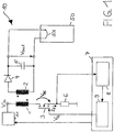
- a heating circuit 10 for preheating or heating a filament 51 of a luminous means 50, such as a gas discharge lamp, with a preferred embodiment of a clocked flyback converter circuit according to the present invention is shown.
- the clocked flyback converter circuit shown comprises a transformer having a primary winding or primary coil 1 and a secondary winding or secondary coil 2, wherein the transformer for transmitting electrical energy from a supplied with an input voltage Vin primary side, which is connected to the primary winding 1 to one with the secondary winding connected secondary side is used to provide an output voltage Vout for heating the heating coil 51 at output terminals.
- the primary side has a controllable power switch 3 connected in series with the primary winding 1, which is realized by a MOS field-effect transistor (MOSFET). In principle, however, other embodiments of the switch 3 are conceivable, such as bipolar transistors or BJT transistors.
- the secondary winding 2 of the transformer is connected in series with a diode 4, which in turn is coupled to a storage capacitor 5, which is arranged in parallel with the output terminals of the flyback converter and provides the output voltage Vout.
- a secondary winding 2 is provided for heating a coil 51.
- two or more secondary windings may be provided with corresponding secondary heating circuits, each of these secondary heating circuits similar to the one in Fig. 1 shown secondary heating circuit and can be connected to a corresponding coil, so that in Fig. 1 shown heating circuit can be easily extended for heating two or more coils.
- the input voltage Vin for the in Fig. 1 The flyback converter circuit shown is supplied by a voltage source 11, which is representative both of a voltage source provided as a separate component and of a circuit portion from which the voltage Vin is derived.
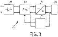
- Fig. 3 shows by way of example the connection of such a heating circuit 10 to an electronic ballast 100.
- the electronic ballast 100 comprises a rectifier circuit 20, which rectifies an input-side supply voltage, such as mains voltage.
- the voltage provided by the rectifier circuit 20 is harmonic filtered in a Power Factor Correction circuit 30 and thus smoothed.
- an inverter circuit 40 is coupled, which converts the intermediate circuit voltage or bus voltage of the power factor correction circuit 30 into an output AC voltage suitable for the operation of the luminous means 50.
- the heating circuit 10 may also be coupled to the power factor correction circuit 30 so that the in Fig. 1 shown input voltage Vin of the intermediate circuit voltage or bus voltage corresponds.
- the switch 3 If the switch 3 is turned off, ie opened, the current drops back to zero. After the switch 3 has been opened, direct current can no longer flow through the switch 3. Due to the magnetization of the transformer then flows on the secondary side via the secondary winding 2, a current until the time of demagnetization of the transformer. At the primary winding 1, high voltages can occur due to the opening of the switch 3, since the current through the primary winding 1 is interrupted abruptly. In addition, a voltage can be fed back from the secondary winding 2.
- the monitoring of the voltage V DS is effected indirectly by detecting the current I S flowing through the switch 3 and the shunt resistor 6. From an evaluation device 8, the current I S is evaluated in the switched-off state of the switch 3 and converted into a corresponding value for the voltage VDS, which is finally compared with the reference value.
- the shunt resistor 6 or the current and voltage values occurring there can also be evaluated for other purposes, for example for overcurrent detection or for detecting the coil 51 connected to the secondary side.
- a further embodiment of the invention is shown, wherein according to Fig. 2 a direct detection of the voltage V DS by means of a parallel to the switch 3 arranged voltage divider, which includes resistors 12 and 13.
- the voltage occurring at the connection point between the resistors 12 and 13 is evaluated by the evaluation device 8 and compared with the reference value.
- the reference value may be in the range of 1200V.
- direct detection of the voltage V DS by the voltage divider may be additionally or alternatively provided to the indirect detection by means of the shunt resistor 6.
- the evaluation device 8 can control a driver device 9 of the control unit 7 that is responsible for the selective switching on and off of the switch 3 such that it switches on again Switch 3 at least temporarily omits or the flyback converter circuit or the heating circuit 10 is completely disabled.
- the evaluation device 8, the driver device 9 also control such that the switch 3 is turned on only with a relation to the normal operation reduced on-time.
- the control unit 7 or the evaluation device 8 the voltage source 11, which provides the input voltage Vin, as in Fig. 1 indicated drives in order to bring about a reduction of the input voltage Vin against the normal operation in error mode.
- the heating circuit 10 as in Fig. 3 shown used in an electronic ballast 100 this can be done for example by appropriate control of serving as a voltage source for the heating circuit 10 power factor correction circuit 30.
- Pulsed current or voltage converter circuits are frequently used as power factor correction circuits 30, so that the reduction of the output voltage of the power factor correction circuit can take place, for example, by appropriate control of a clocking controllable switch of the power factor correction circuit.
- the clocked flyback converter circuit it is also possible for the clocked flyback converter circuit to be used for the direct or indirect supply of a light-emitting diode (LED).
- LED light-emitting diode
- one or more light emitting diodes may be connected to the secondary side of the transformer.
- the clocked flyback converter circuit it would also be possible for the clocked flyback converter circuit to supply a downstream DC-DC converter, for example a clocked constant-current source, and this downstream DC-DC converter serves to supply one or more light-emitting diodes.
- a DC-DC converter can be for example a buck converter or a resonant half-bridge circuit, preferably with current regulation.
- the falling over the shunt resistor 6 Voltage is monitored by the monitoring device 8 of the control unit 7 and the monitoring device 8 detects in particular when a zero crossing of the current I S due to the demagnetization of the transformer after a switch-off of the switch 3 occurs. Only upon detection of such a zero crossing, a control signal for a driver device 9 is generated by the monitoring device 8 to cause them to adjust the gate voltage V G of the switch 3 to turn on the switch 3 again.
- This type of control can be used to provide the most trouble-free and loss-free switching of the switch 3 and also independent of the winding capacity, which can vary over a wide range, provide a possible non-varying output current.
- the monitoring of the switch current I S takes place with the aid of the shunt resistor 6, the voltage occurring at the shunt resistor 6 being evaluated in the monitoring device 8.
- the shunt resistor 6 or the current and voltage values occurring there can also be evaluated for other purposes, for example for overcurrent detection or for detecting the load connected to the secondary side, ie in the illustrated example of the heating circuit 10 for detecting the respectively connected to be heated Spiral 51 or in the case of a light-emitting diode as a load Typerkennung for example, the color or the power of the light emitting diode.
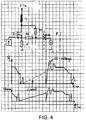
- Fig. 4 is a schematic representation of a clocked flyback converter circuit according to another embodiment of the invention shown.
- the clocked flyback converter circuit shown comprises a transformer with a primary winding or primary coil 1 and a secondary winding or secondary coil 2 (not illustrated here).
- the transformer is used to transmit electrical energy from a primary side supplied with an input voltage Vin, which is connected to the primary winding 1, to a secondary side connected to the secondary winding 2, in order to provide at output terminals an output voltage Vout, for example, for heating a heating coil or for supplying a light emitting diode available.
- the primary side has a controllable power switch 3 connected in series with the primary winding 1, which is realized here by a MOS field-effect transistor (MOSFET).
- MOSFET MOS field-effect transistor
- the controllable switch 3 is driven by a control unit 7, which selectively turns it on in normal operation by appropriate adjustment of the gate voltage V G of the designed as a MOSFET switch 3 for clocking the flyback converter with a specific frequency and duty cycle and off again.
- Fig. 4 connected to ground shunt resistor 6 connected.
- a resistor R1 is arranged.
- This resistor R1 is connected to the primary winding 1 with a connection to the connection point of the switch 3.
- the other terminal of the resistor R1 is connected to a measuring input of the control unit 7 and the evaluation device 8 and to a further resistor R2.
- the further resistor R2 is connected on the one hand to a terminal of the resistor R1 and the other with the connection point of the shunt resistor 6 and switch 3.
- the two resistors R1 and R2 are designed relatively high impedance compared to the shunt resistor 6. In this example, therefore, there is a direct detection of the voltage VDS across the switch 3.
- the switch 3 If the switch 3 is turned on, flows over the primary winding 1 and the switch 3 is a linearly increasing current I S , so that electric energy is stored in the primary winding 1 (it is magnetized). This current flow can be detected by shunt resistor 6.
- the parallel resistor R1 is bridged in this phase by the very low-resistance switch 3, as long as the switch 3 is turned on. When opening the switch 3 this is very high, now can be detected by the evaluation device 8 via the resistor divider R1, R2 and 6, the voltage drop across the switch 3 voltage by means of the measuring input Sense.
- Fig. 4 Below is the course of the voltage detected at the Sense input.
- the resistors R1 and R2 are used as an ohmic voltage divider, while in the example of the Fig. 1 the parasitic capacitances of the switched off switch 3 are used to close the voltage across the switch 3.
- the example of Fig. 2 allows the example of Fig. 4 a reduction of the inputs required at the evaluation device 8.
- the invention may also relate to a non-isolated flyback converter circuit.
- a non-isolated flyback converter circuit instead of the transformer only one coil is present as an inductance, which takes over both the function of the primary winding and the secondary winding of the transformer.
- there is a clocked flyback converter circuit which has an inductance, wherein the clocked flyback converter circuit is configured such that it transfers electrical energy in a normal operation by repeated switching on and off of a connected to the inductance switch 3, and a control unit 7 for driving of the switch 3 of the clocked flyback converter circuit.
- the inductance By repeatedly turning on and off the switch 3, the inductance is up and demagnetized and thus transmit electrical energy.
- a detection device 6; 10, 11 for directly or indirectly detecting a voltage at the switch 3 after turning off the switch 3 is present.
- an evaluation device 8 is present for comparing the voltage detected by the detection device 6 after switching off the switch 3 on the switch 3 with a reference value to a change from the normal operation to cause an error operation, if the voltage at the switch 3 exceeds the reference value.
- the evaluation device 8 may be provided as part of the control unit 7, wherein the control unit 7 preferably in the form of an integrated circuit, in particular as an ASIC ("Application Specific Integrated Circuit") is configured. However, it is also possible that the evaluation device 8 is a separate component from the control unit 7.
Landscapes
- Engineering & Computer Science (AREA)
- Power Engineering (AREA)
- Dc-Dc Converters (AREA)
Claims (12)
- Procédé de commutation d'un circuit convertisseur à transfert indirect cadencé, le circuit convertisseur à transfert indirect comprenant un transformateur doté d'un enroulement primaire (1) et d'un enroulement secondaire (2), et de l'énergie électrique étant, en mode normal, transmise à partir d'un côté primaire connecté à l'enroulement primaire (1), et cadencé avec un commutateur (3) par mise en circuit et mise hors circuit répétées du commutateur (3), vers un côté secondaire connecté à l'enroulement secondaire (2),
comportant les étapes suivantes :détection d'une tension (VDS) sur le commutateur (3),comparaison de la tension (VDS) sur le commutateur (3) avec une valeur de référence, etpassage du mode normal à un mode d'erreur si la tension (VDS) sur le commutateur (3) dépasse la valeur de référence,caractérisé en ce quela détection de la tension (VDS) sur le commutateur (3) s'effectue après la mise hors circuit du commutateur (3),la tension (VDS) sur le commutateur (3) étant détectée par la détection d'un courant (IS) traversant une résistance (6) montée entre le commutateur (3) et la masse, etle courant (IS) traversant la résistance (6) étant analysé en outre pour la détection d'une charge (51) connectée au côté secondaire ou pour la détection de surintensité. - Procédé selon la revendication 1,
caractérisé en ce que,
dans le mode d'erreur, une mise en circuit du commutateur (3) est interdite au moins provisoirement, ou bien un temps de mise en circuit du commutateur (3) est réduit par rapport au mode normal. - Procédé selon la revendication 1 ou 2,
caractérisé en ce que,
dans le mode d'erreur, une tension d'alimentation (Vin) présente sur le côté primaire du circuit convertisseur à transfert indirect cadencé est réduite par rapport au mode normal. - Procédé selon la revendication 3,
caractérisé en ce que
la tension d'alimentation (Vin) est mise à disposition par un circuit de correction du facteur de puissance (30) couplé au circuit convertisseur à transfert indirect cadencé, le circuit de correction du facteur de puissance (30) étant, dans le mode d'erreur, piloté en vue de la réduction de la tension d'alimentation (Vin) par rapport au mode normal. - Circuit convertisseur à transfert indirect cadencé, comprenant
un transformateur doté d'un enroulement primaire (1) et d'un enroulement secondaire (2), le circuit convertisseur à transfert indirect cadencé étant constitué de telle sorte que, dans un mode normal, il transmet de l'énergie électrique à partir d'un côté primaire connecté à l'enroulement primaire (1), et cadencé avec un commutateur (3) par mise en circuit et mise hors circuit répétées du commutateur (3), vers un côté secondaire connecté à l'enroulement secondaire (2),
une unité de commande (7) destinée au pilotage du commutateur (3) du circuit convertisseur à transfert indirect cadencé,
un dispositif de détection (6 ; 10, 11) destiné à la détection d'une tension (VDS) sur le commutateur (3), et
un dispositif d'analyse (8) destiné à la comparaison de la tension (VDS) sur le commutateur (3) détectée par le dispositif de détection (6 ; 10, 11) avec une valeur de référence pour provoquer un passage du mode normal vers un mode d'erreur si la tension (VDS) sur le commutateur (3) dépasse la valeur de référence,
caractérisé en ce que
le dispositif de détection (6 ; 10, 11) est agencé de telle sorte qu'il détecte la tension (VDS) sur le commutateur (3) après la mise hors circuit du commutateur (3), le dispositif de détection comprenant une résistance (6) montée entre le commutateur (3) et la masse pour la détection d'un courant (IS) traversant le commutateur en tant que grandeur représentant la tension (VDS) sur le commutateur (3),
le dispositif d'analyse (8) analysant le courant (Is) traversant la résistance (6) en outre pour la détection d'une charge (51) connectée au côté secondaire ou pour la détection de surintensité. - Circuit convertisseur à transfert indirect cadencé selon la revendication 5,
caractérisé en ce que,
dans le mode d'erreur, le dispositif d'analyse (8) interdit au moins provisoirement une mise en circuit du commutateur (3) par l'unité de commande (7) ou bien provoque une réduction du temps de mise en circuit du commutateur (3) par rapport au mode normal. - Circuit convertisseur à transfert indirect cadencé selon la revendication 5 ou 6,
caractérisé en ce que
le dispositif d'analyse (8) est constitué de telle sorte que, dans le mode d'erreur, pour la réduction de la tension d'alimentation (Vin) par rapport au mode normal, il pilote une source de tension d'alimentation (11 ; 30) qui met à disposition une tension d'alimentation (Vin) présente sur le côté primaire du circuit convertisseur à transfert indirect cadencé. - Circuit convertisseur à transfert indirect cadencé selon l'une des revendications 5 à 7,
caractérisé en ce que
le dispositif d'analyse (8) fait partie de l'unité de commande (7) constituée sous la forme d'un circuit intégré. - Circuit convertisseur à transfert indirect cadencé selon l'une des revendications 5 à 8,
caractérisé en ce que
le commutateur (3) est un transistor à effet de champ MOS, la tension (VDS) détectée par le dispositif de détection (6 ; 10, 11) étant une tension drain-source du transistor à effet de champ MOS. - Circuit convertisseur à transfert indirect cadencé selon l'une des revendications 5 à 9,
caractérisé en ce que
le dispositif de détection comprend un circuit diviseur de tension (12, 13) couplé au commutateur (3), qui est en particulier disposé en parallèle avec le commutateur (3), pour la détection de la tension sur le commutateur (3). - Circuit convertisseur à transfert indirect cadencé selon l'une des revendications 5 à 10,
caractérisé en ce que
le circuit convertisseur à transfert indirect cadencé est constitué en tant que circuit de chauffage (10) destiné à chauffer au moins un filament (51) d'une lampe à décharge ou d'une lampe fluorescente (50). - Appareil de manoeuvre ou ballast électronique (100) pour un moyen d'éclairage (50) avec un circuit convertisseur à transfert indirect cadencé selon l'une des revendications 5 à 11.
Applications Claiming Priority (2)
| Application Number | Priority Date | Filing Date | Title |
|---|---|---|---|
| DE102011103409A DE102011103409A1 (de) | 2011-06-06 | 2011-06-06 | Verfahren zum Heizen einer Wendel eines Leuchtmittels und entsprechende Heizschaltung |
| PCT/AT2012/000157 WO2012167293A1 (fr) | 2011-06-06 | 2012-06-06 | Procédé de connexion d'un circuit convertisseur à transfert indirect cadencé |
Publications (2)
| Publication Number | Publication Date |
|---|---|
| EP2719064A1 EP2719064A1 (fr) | 2014-04-16 |
| EP2719064B1 true EP2719064B1 (fr) | 2018-11-28 |
Family
ID=46614258
Family Applications (1)
| Application Number | Title | Priority Date | Filing Date |
|---|---|---|---|
| EP12743349.8A Not-in-force EP2719064B1 (fr) | 2011-06-06 | 2012-06-06 | Procédé de connexion d'un circuit convertisseur à transfert indirect cadencé |
Country Status (3)
| Country | Link |
|---|---|
| EP (1) | EP2719064B1 (fr) |
| DE (1) | DE102011103409A1 (fr) |
| WO (1) | WO2012167293A1 (fr) |
Families Citing this family (1)
| Publication number | Priority date | Publication date | Assignee | Title |
|---|---|---|---|---|
| DE102014217688A1 (de) | 2014-09-04 | 2016-03-10 | Tridonic Gmbh & Co Kg | Betriebsgerät für Leuchtmittel |
Family Cites Families (6)
| Publication number | Priority date | Publication date | Assignee | Title |
|---|---|---|---|---|
| JPH05146149A (ja) * | 1991-11-20 | 1993-06-11 | Murata Mfg Co Ltd | スイツチング電源装置 |
| JPH06201738A (ja) * | 1993-01-06 | 1994-07-22 | Mitsubishi Electric Corp | 電流検出回路 |
| US5703441A (en) * | 1995-11-02 | 1997-12-30 | General Electric Company | Multi-function filament-heater power supply for an electronic ballast for long-life dimmerable lamps |
| JP2972653B2 (ja) * | 1997-06-09 | 1999-11-08 | 甲府日本電気株式会社 | 電源故障検出回路 |
| US6396718B1 (en) * | 2000-12-19 | 2002-05-28 | Semiconductor Components Industries Llc | Switch mode power supply using transformer flux sensing for duty cycle control |
| DE102005018761A1 (de) * | 2005-04-22 | 2006-10-26 | Tridonicatco Gmbh & Co. Kg | Intelligente Flyback-Heizung |
-
2011
- 2011-06-06 DE DE102011103409A patent/DE102011103409A1/de not_active Withdrawn
-
2012
- 2012-06-06 EP EP12743349.8A patent/EP2719064B1/fr not_active Not-in-force
- 2012-06-06 WO PCT/AT2012/000157 patent/WO2012167293A1/fr not_active Ceased
Non-Patent Citations (1)
| Title |
|---|
| None * |
Also Published As
| Publication number | Publication date |
|---|---|
| WO2012167293A1 (fr) | 2012-12-13 |
| EP2719064A1 (fr) | 2014-04-16 |
| DE102011103409A1 (de) | 2012-12-06 |
Similar Documents
| Publication | Publication Date | Title |
|---|---|---|
| EP2345308B1 (fr) | Circuit de fonctionnement destiné à des led | |
| EP2888800B1 (fr) | Appareil de lumière de secours | |
| DE102012007478B4 (de) | Wandler für ein Leuchtmittel, LED-Konverter und Verfahren zum Betreiben eines Wandlers | |
| EP2829157B1 (fr) | Circuit de commande pour diodes électroluminescentes avec signal de variation de lumière issu d`un signal en trains d'impulsions modulés a haute fréquence, avec des fréquences accordées | |
| EP4221464B1 (fr) | Circuit convertisseur à découpage à verrouillage | |
| EP2891382B1 (fr) | Appareil de commande permettant de commander une ligne de del | |
| WO2014176609A1 (fr) | Circuit d'exploitation pour diodes électroluminescentes | |
| DE10310764B4 (de) | Gleichspannungswandler einer Entladungslampe | |
| AT16263U1 (de) | PFC-Schaltung mit spannungsabhängiger Signalzuführung | |
| EP2719064B1 (fr) | Procédé de connexion d'un circuit convertisseur à transfert indirect cadencé | |
| EP2719065B1 (fr) | Procédé de connexion d'un circuit convertisseur à transfert indirect cadencé, et circuit convertisseur à transfert indirect | |
| EP3782274B1 (fr) | Circuit de fonctionnement pour charges à led, présentant un circuit en demi-pont | |
| AT12495U1 (de) | Fehlererkennung für leuchtdioden | |
| EP2992738B1 (fr) | Reconnaissance d'erreur pour del | |
| EP2961049B1 (fr) | Commutateur de commande d'un convertisseur de courant à résonance | |
| AT13450U1 (de) | Betriebsschaltung für Leuchtdioden | |
| EP3449692A1 (fr) | Procédé de réglage d'un module del | |
| EP2132965A1 (fr) | Circuit pour le chauffage d'un filament | |
| DE102015206982B4 (de) | Leuchtmittelkonverter mit symmetrierten Ausgangsströmen sowie Verfahren zum Symmetrieren | |
| DE102015217146A1 (de) | Getaktete Sperrwandlerschaltung | |
| WO2019211129A1 (fr) | Appareil de fonctionnement pour un moyen d'éclairage avec un convertisseur à résonance et une commande de luminosité | |
| DE102014108775A1 (de) | Tiefsetzer sowie LED-Einrichtung, insbesondere LED-Scheinwerfer oder LED-Signallicht, mit einem solchen Tiefsetzer | |
| EP1860925B1 (fr) | Appareil de montage de lampe électronique à connexion à chaud | |
| EP2208402B1 (fr) | Ballast pour lampe à décharge, par exemple pour une lampe dhi | |
| WO2011130770A1 (fr) | Ballast pour diodes électroluminescentes |
Legal Events
| Date | Code | Title | Description |
|---|---|---|---|
| PUAI | Public reference made under article 153(3) epc to a published international application that has entered the european phase |
Free format text: ORIGINAL CODE: 0009012 |
|
| 17P | Request for examination filed |
Effective date: 20131210 |
|
| AK | Designated contracting states |
Kind code of ref document: A1 Designated state(s): AL AT BE BG CH CY CZ DE DK EE ES FI FR GB GR HR HU IE IS IT LI LT LU LV MC MK MT NL NO PL PT RO RS SE SI SK SM TR |
|
| DAX | Request for extension of the european patent (deleted) | ||
| STAA | Information on the status of an ep patent application or granted ep patent |
Free format text: STATUS: EXAMINATION IS IN PROGRESS |
|
| 17Q | First examination report despatched |
Effective date: 20170901 |
|
| GRAP | Despatch of communication of intention to grant a patent |
Free format text: ORIGINAL CODE: EPIDOSNIGR1 |
|
| STAA | Information on the status of an ep patent application or granted ep patent |
Free format text: STATUS: GRANT OF PATENT IS INTENDED |
|
| INTG | Intention to grant announced |
Effective date: 20180903 |
|
| GRAS | Grant fee paid |
Free format text: ORIGINAL CODE: EPIDOSNIGR3 |
|
| GRAA | (expected) grant |
Free format text: ORIGINAL CODE: 0009210 |
|
| STAA | Information on the status of an ep patent application or granted ep patent |
Free format text: STATUS: THE PATENT HAS BEEN GRANTED |
|
| AK | Designated contracting states |
Kind code of ref document: B1 Designated state(s): AL AT BE BG CH CY CZ DE DK EE ES FI FR GB GR HR HU IE IS IT LI LT LU LV MC MK MT NL NO PL PT RO RS SE SI SK SM TR |
|
| REG | Reference to a national code |
Ref country code: GB Ref legal event code: FG4D Free format text: NOT ENGLISH |
|
| REG | Reference to a national code |
Ref country code: CH Ref legal event code: EP |
|
| REG | Reference to a national code |
Ref country code: DE Ref legal event code: R096 Ref document number: 502012013912 Country of ref document: DE |
|
| REG | Reference to a national code |
Ref country code: AT Ref legal event code: REF Ref document number: 1071408 Country of ref document: AT Kind code of ref document: T Effective date: 20181215 |
|
| REG | Reference to a national code |
Ref country code: IE Ref legal event code: FG4D Free format text: LANGUAGE OF EP DOCUMENT: GERMAN |
|
| REG | Reference to a national code |
Ref country code: NL Ref legal event code: MP Effective date: 20181128 |
|
| REG | Reference to a national code |
Ref country code: LT Ref legal event code: MG4D |
|
| PG25 | Lapsed in a contracting state [announced via postgrant information from national office to epo] |
Ref country code: ES Free format text: LAPSE BECAUSE OF FAILURE TO SUBMIT A TRANSLATION OF THE DESCRIPTION OR TO PAY THE FEE WITHIN THE PRESCRIBED TIME-LIMIT Effective date: 20181128 Ref country code: LV Free format text: LAPSE BECAUSE OF FAILURE TO SUBMIT A TRANSLATION OF THE DESCRIPTION OR TO PAY THE FEE WITHIN THE PRESCRIBED TIME-LIMIT Effective date: 20181128 Ref country code: FI Free format text: LAPSE BECAUSE OF FAILURE TO SUBMIT A TRANSLATION OF THE DESCRIPTION OR TO PAY THE FEE WITHIN THE PRESCRIBED TIME-LIMIT Effective date: 20181128 Ref country code: IS Free format text: LAPSE BECAUSE OF FAILURE TO SUBMIT A TRANSLATION OF THE DESCRIPTION OR TO PAY THE FEE WITHIN THE PRESCRIBED TIME-LIMIT Effective date: 20190328 Ref country code: BG Free format text: LAPSE BECAUSE OF FAILURE TO SUBMIT A TRANSLATION OF THE DESCRIPTION OR TO PAY THE FEE WITHIN THE PRESCRIBED TIME-LIMIT Effective date: 20190228 Ref country code: HR Free format text: LAPSE BECAUSE OF FAILURE TO SUBMIT A TRANSLATION OF THE DESCRIPTION OR TO PAY THE FEE WITHIN THE PRESCRIBED TIME-LIMIT Effective date: 20181128 Ref country code: NO Free format text: LAPSE BECAUSE OF FAILURE TO SUBMIT A TRANSLATION OF THE DESCRIPTION OR TO PAY THE FEE WITHIN THE PRESCRIBED TIME-LIMIT Effective date: 20190228 Ref country code: LT Free format text: LAPSE BECAUSE OF FAILURE TO SUBMIT A TRANSLATION OF THE DESCRIPTION OR TO PAY THE FEE WITHIN THE PRESCRIBED TIME-LIMIT Effective date: 20181128 |
|
| PG25 | Lapsed in a contracting state [announced via postgrant information from national office to epo] |
Ref country code: SE Free format text: LAPSE BECAUSE OF FAILURE TO SUBMIT A TRANSLATION OF THE DESCRIPTION OR TO PAY THE FEE WITHIN THE PRESCRIBED TIME-LIMIT Effective date: 20181128 Ref country code: RS Free format text: LAPSE BECAUSE OF FAILURE TO SUBMIT A TRANSLATION OF THE DESCRIPTION OR TO PAY THE FEE WITHIN THE PRESCRIBED TIME-LIMIT Effective date: 20181128 Ref country code: PT Free format text: LAPSE BECAUSE OF FAILURE TO SUBMIT A TRANSLATION OF THE DESCRIPTION OR TO PAY THE FEE WITHIN THE PRESCRIBED TIME-LIMIT Effective date: 20190328 Ref country code: GR Free format text: LAPSE BECAUSE OF FAILURE TO SUBMIT A TRANSLATION OF THE DESCRIPTION OR TO PAY THE FEE WITHIN THE PRESCRIBED TIME-LIMIT Effective date: 20190301 Ref country code: AL Free format text: LAPSE BECAUSE OF FAILURE TO SUBMIT A TRANSLATION OF THE DESCRIPTION OR TO PAY THE FEE WITHIN THE PRESCRIBED TIME-LIMIT Effective date: 20181128 |
|
| PG25 | Lapsed in a contracting state [announced via postgrant information from national office to epo] |
Ref country code: NL Free format text: LAPSE BECAUSE OF FAILURE TO SUBMIT A TRANSLATION OF THE DESCRIPTION OR TO PAY THE FEE WITHIN THE PRESCRIBED TIME-LIMIT Effective date: 20181128 |
|
| PG25 | Lapsed in a contracting state [announced via postgrant information from national office to epo] |
Ref country code: PL Free format text: LAPSE BECAUSE OF FAILURE TO SUBMIT A TRANSLATION OF THE DESCRIPTION OR TO PAY THE FEE WITHIN THE PRESCRIBED TIME-LIMIT Effective date: 20181128 Ref country code: CZ Free format text: LAPSE BECAUSE OF FAILURE TO SUBMIT A TRANSLATION OF THE DESCRIPTION OR TO PAY THE FEE WITHIN THE PRESCRIBED TIME-LIMIT Effective date: 20181128 Ref country code: IT Free format text: LAPSE BECAUSE OF FAILURE TO SUBMIT A TRANSLATION OF THE DESCRIPTION OR TO PAY THE FEE WITHIN THE PRESCRIBED TIME-LIMIT Effective date: 20181128 Ref country code: DK Free format text: LAPSE BECAUSE OF FAILURE TO SUBMIT A TRANSLATION OF THE DESCRIPTION OR TO PAY THE FEE WITHIN THE PRESCRIBED TIME-LIMIT Effective date: 20181128 |
|
| REG | Reference to a national code |
Ref country code: DE Ref legal event code: R097 Ref document number: 502012013912 Country of ref document: DE |
|
| PG25 | Lapsed in a contracting state [announced via postgrant information from national office to epo] |
Ref country code: SK Free format text: LAPSE BECAUSE OF FAILURE TO SUBMIT A TRANSLATION OF THE DESCRIPTION OR TO PAY THE FEE WITHIN THE PRESCRIBED TIME-LIMIT Effective date: 20181128 Ref country code: RO Free format text: LAPSE BECAUSE OF FAILURE TO SUBMIT A TRANSLATION OF THE DESCRIPTION OR TO PAY THE FEE WITHIN THE PRESCRIBED TIME-LIMIT Effective date: 20181128 Ref country code: EE Free format text: LAPSE BECAUSE OF FAILURE TO SUBMIT A TRANSLATION OF THE DESCRIPTION OR TO PAY THE FEE WITHIN THE PRESCRIBED TIME-LIMIT Effective date: 20181128 Ref country code: SM Free format text: LAPSE BECAUSE OF FAILURE TO SUBMIT A TRANSLATION OF THE DESCRIPTION OR TO PAY THE FEE WITHIN THE PRESCRIBED TIME-LIMIT Effective date: 20181128 |
|
| PLBE | No opposition filed within time limit |
Free format text: ORIGINAL CODE: 0009261 |
|
| STAA | Information on the status of an ep patent application or granted ep patent |
Free format text: STATUS: NO OPPOSITION FILED WITHIN TIME LIMIT |
|
| PG25 | Lapsed in a contracting state [announced via postgrant information from national office to epo] |
Ref country code: SI Free format text: LAPSE BECAUSE OF FAILURE TO SUBMIT A TRANSLATION OF THE DESCRIPTION OR TO PAY THE FEE WITHIN THE PRESCRIBED TIME-LIMIT Effective date: 20181128 |
|
| 26N | No opposition filed |
Effective date: 20190829 |
|
| PG25 | Lapsed in a contracting state [announced via postgrant information from national office to epo] |
Ref country code: MC Free format text: LAPSE BECAUSE OF FAILURE TO SUBMIT A TRANSLATION OF THE DESCRIPTION OR TO PAY THE FEE WITHIN THE PRESCRIBED TIME-LIMIT Effective date: 20181128 |
|
| REG | Reference to a national code |
Ref country code: CH Ref legal event code: PL |
|
| REG | Reference to a national code |
Ref country code: BE Ref legal event code: MM Effective date: 20190630 |
|
| PG25 | Lapsed in a contracting state [announced via postgrant information from national office to epo] |
Ref country code: TR Free format text: LAPSE BECAUSE OF FAILURE TO SUBMIT A TRANSLATION OF THE DESCRIPTION OR TO PAY THE FEE WITHIN THE PRESCRIBED TIME-LIMIT Effective date: 20181128 |
|
| PG25 | Lapsed in a contracting state [announced via postgrant information from national office to epo] |
Ref country code: IE Free format text: LAPSE BECAUSE OF NON-PAYMENT OF DUE FEES Effective date: 20190606 |
|
| PG25 | Lapsed in a contracting state [announced via postgrant information from national office to epo] |
Ref country code: LI Free format text: LAPSE BECAUSE OF NON-PAYMENT OF DUE FEES Effective date: 20190630 Ref country code: LU Free format text: LAPSE BECAUSE OF NON-PAYMENT OF DUE FEES Effective date: 20190606 Ref country code: CH Free format text: LAPSE BECAUSE OF NON-PAYMENT OF DUE FEES Effective date: 20190630 Ref country code: BE Free format text: LAPSE BECAUSE OF NON-PAYMENT OF DUE FEES Effective date: 20190630 |
|
| PGFP | Annual fee paid to national office [announced via postgrant information from national office to epo] |
Ref country code: AT Payment date: 20200622 Year of fee payment: 9 |
|
| PG25 | Lapsed in a contracting state [announced via postgrant information from national office to epo] |
Ref country code: CY Free format text: LAPSE BECAUSE OF FAILURE TO SUBMIT A TRANSLATION OF THE DESCRIPTION OR TO PAY THE FEE WITHIN THE PRESCRIBED TIME-LIMIT Effective date: 20181128 |
|
| PG25 | Lapsed in a contracting state [announced via postgrant information from national office to epo] |
Ref country code: MT Free format text: LAPSE BECAUSE OF FAILURE TO SUBMIT A TRANSLATION OF THE DESCRIPTION OR TO PAY THE FEE WITHIN THE PRESCRIBED TIME-LIMIT Effective date: 20181128 Ref country code: HU Free format text: LAPSE BECAUSE OF FAILURE TO SUBMIT A TRANSLATION OF THE DESCRIPTION OR TO PAY THE FEE WITHIN THE PRESCRIBED TIME-LIMIT; INVALID AB INITIO Effective date: 20120606 |
|
| REG | Reference to a national code |
Ref country code: AT Ref legal event code: MM01 Ref document number: 1071408 Country of ref document: AT Kind code of ref document: T Effective date: 20210606 |
|
| PG25 | Lapsed in a contracting state [announced via postgrant information from national office to epo] |
Ref country code: AT Free format text: LAPSE BECAUSE OF NON-PAYMENT OF DUE FEES Effective date: 20210606 |
|
| PG25 | Lapsed in a contracting state [announced via postgrant information from national office to epo] |
Ref country code: MK Free format text: LAPSE BECAUSE OF FAILURE TO SUBMIT A TRANSLATION OF THE DESCRIPTION OR TO PAY THE FEE WITHIN THE PRESCRIBED TIME-LIMIT Effective date: 20181128 |
|
| PGFP | Annual fee paid to national office [announced via postgrant information from national office to epo] |
Ref country code: FR Payment date: 20220623 Year of fee payment: 11 |
|
| REG | Reference to a national code |
Ref country code: DE Ref legal event code: R084 Ref document number: 502012013912 Country of ref document: DE |
|
| P01 | Opt-out of the competence of the unified patent court (upc) registered |
Effective date: 20230530 |
|
| PG25 | Lapsed in a contracting state [announced via postgrant information from national office to epo] |
Ref country code: FR Free format text: LAPSE BECAUSE OF NON-PAYMENT OF DUE FEES Effective date: 20230630 |
|
| PGFP | Annual fee paid to national office [announced via postgrant information from national office to epo] |
Ref country code: GB Payment date: 20240618 Year of fee payment: 13 |
|
| PGFP | Annual fee paid to national office [announced via postgrant information from national office to epo] |
Ref country code: DE Payment date: 20240627 Year of fee payment: 13 |
|
| REG | Reference to a national code |
Ref country code: DE Ref legal event code: R119 Ref document number: 502012013912 Country of ref document: DE |
|
| GBPC | Gb: european patent ceased through non-payment of renewal fee |
Effective date: 20250606 |
|
| PG25 | Lapsed in a contracting state [announced via postgrant information from national office to epo] |
Ref country code: GB Free format text: LAPSE BECAUSE OF NON-PAYMENT OF DUE FEES Effective date: 20250606 |
|
| PG25 | Lapsed in a contracting state [announced via postgrant information from national office to epo] |
Ref country code: DE Free format text: LAPSE BECAUSE OF NON-PAYMENT OF DUE FEES Effective date: 20260101 |