EP2719460B1 - Dispositifs microfluidiques - Google Patents
Dispositifs microfluidiques Download PDFInfo
- Publication number
- EP2719460B1 EP2719460B1 EP13187740.9A EP13187740A EP2719460B1 EP 2719460 B1 EP2719460 B1 EP 2719460B1 EP 13187740 A EP13187740 A EP 13187740A EP 2719460 B1 EP2719460 B1 EP 2719460B1
- Authority
- EP
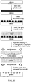
- European Patent Office
- Prior art keywords
- substrates
- substrate
- microfluidic circuit
- interface
- microfluidic
- Prior art date
- Legal status (The legal status is an assumption and is not a legal conclusion. Google has not performed a legal analysis and makes no representation as to the accuracy of the status listed.)
- Active
Links
Images




Classifications
-
- G—PHYSICS
- G05—CONTROLLING; REGULATING
- G05D—SYSTEMS FOR CONTROLLING OR REGULATING NON-ELECTRIC VARIABLES
- G05D7/00—Control of flow
- G05D7/06—Control of flow characterised by the use of electric means
- G05D7/0617—Control of flow characterised by the use of electric means specially adapted for fluid materials
- G05D7/0629—Control of flow characterised by the use of electric means specially adapted for fluid materials characterised by the type of regulator means
- G05D7/0694—Control of flow characterised by the use of electric means specially adapted for fluid materials characterised by the type of regulator means by action on throttling means or flow sources of very small size, e.g. microfluidics
-
- B—PERFORMING OPERATIONS; TRANSPORTING
- B01—PHYSICAL OR CHEMICAL PROCESSES OR APPARATUS IN GENERAL
- B01L—CHEMICAL OR PHYSICAL LABORATORY APPARATUS FOR GENERAL USE
- B01L3/00—Containers or dishes for laboratory use, e.g. laboratory glassware; Droppers
- B01L3/50—Containers for the purpose of retaining a material to be analysed, e.g. test tubes
- B01L3/502—Containers for the purpose of retaining a material to be analysed, e.g. test tubes with fluid transport, e.g. in multi-compartment structures
- B01L3/5027—Containers for the purpose of retaining a material to be analysed, e.g. test tubes with fluid transport, e.g. in multi-compartment structures by integrated microfluidic structures, i.e. dimensions of channels and chambers are such that surface tension forces are important, e.g. lab-on-a-chip
- B01L3/502707—Containers for the purpose of retaining a material to be analysed, e.g. test tubes with fluid transport, e.g. in multi-compartment structures by integrated microfluidic structures, i.e. dimensions of channels and chambers are such that surface tension forces are important, e.g. lab-on-a-chip characterised by the manufacture of the container or its components
-
- B—PERFORMING OPERATIONS; TRANSPORTING
- B29—WORKING OF PLASTICS; WORKING OF SUBSTANCES IN A PLASTIC STATE IN GENERAL
- B29C—SHAPING OR JOINING OF PLASTICS; SHAPING OF MATERIAL IN A PLASTIC STATE, NOT OTHERWISE PROVIDED FOR; AFTER-TREATMENT OF THE SHAPED PRODUCTS, e.g. REPAIRING
- B29C65/00—Joining or sealing of preformed parts, e.g. welding of plastics materials; Apparatus therefor
- B29C65/02—Joining or sealing of preformed parts, e.g. welding of plastics materials; Apparatus therefor by heating, with or without pressure
- B29C65/14—Joining or sealing of preformed parts, e.g. welding of plastics materials; Apparatus therefor by heating, with or without pressure using wave energy, i.e. electromagnetic radiation, or particle radiation
- B29C65/16—Laser beams
- B29C65/1629—Laser beams characterised by the way of heating the interface
- B29C65/1635—Laser beams characterised by the way of heating the interface at least passing through one of the parts to be joined, i.e. laser transmission welding
- B29C65/1638—Laser beams characterised by the way of heating the interface at least passing through one of the parts to be joined, i.e. laser transmission welding focusing the laser beam on the interface
-
- B—PERFORMING OPERATIONS; TRANSPORTING
- B29—WORKING OF PLASTICS; WORKING OF SUBSTANCES IN A PLASTIC STATE IN GENERAL
- B29C—SHAPING OR JOINING OF PLASTICS; SHAPING OF MATERIAL IN A PLASTIC STATE, NOT OTHERWISE PROVIDED FOR; AFTER-TREATMENT OF THE SHAPED PRODUCTS, e.g. REPAIRING
- B29C65/00—Joining or sealing of preformed parts, e.g. welding of plastics materials; Apparatus therefor
- B29C65/02—Joining or sealing of preformed parts, e.g. welding of plastics materials; Apparatus therefor by heating, with or without pressure
- B29C65/14—Joining or sealing of preformed parts, e.g. welding of plastics materials; Apparatus therefor by heating, with or without pressure using wave energy, i.e. electromagnetic radiation, or particle radiation
- B29C65/16—Laser beams
- B29C65/1629—Laser beams characterised by the way of heating the interface
- B29C65/1654—Laser beams characterised by the way of heating the interface scanning at least one of the parts to be joined
-
- B—PERFORMING OPERATIONS; TRANSPORTING
- B29—WORKING OF PLASTICS; WORKING OF SUBSTANCES IN A PLASTIC STATE IN GENERAL
- B29C—SHAPING OR JOINING OF PLASTICS; SHAPING OF MATERIAL IN A PLASTIC STATE, NOT OTHERWISE PROVIDED FOR; AFTER-TREATMENT OF THE SHAPED PRODUCTS, e.g. REPAIRING
- B29C66/00—General aspects of processes or apparatus for joining preformed parts
- B29C66/01—General aspects dealing with the joint area or with the area to be joined
- B29C66/05—Particular design of joint configurations
- B29C66/10—Particular design of joint configurations particular design of the joint cross-sections
- B29C66/11—Joint cross-sections comprising a single joint-segment, i.e. one of the parts to be joined comprising a single joint-segment in the joint cross-section
- B29C66/112—Single lapped joints
- B29C66/1122—Single lap to lap joints, i.e. overlap joints
-
- B—PERFORMING OPERATIONS; TRANSPORTING
- B29—WORKING OF PLASTICS; WORKING OF SUBSTANCES IN A PLASTIC STATE IN GENERAL
- B29C—SHAPING OR JOINING OF PLASTICS; SHAPING OF MATERIAL IN A PLASTIC STATE, NOT OTHERWISE PROVIDED FOR; AFTER-TREATMENT OF THE SHAPED PRODUCTS, e.g. REPAIRING
- B29C66/00—General aspects of processes or apparatus for joining preformed parts
- B29C66/01—General aspects dealing with the joint area or with the area to be joined
- B29C66/05—Particular design of joint configurations
- B29C66/20—Particular design of joint configurations particular design of the joint lines, e.g. of the weld lines
- B29C66/24—Particular design of joint configurations particular design of the joint lines, e.g. of the weld lines said joint lines being closed or non-straight
- B29C66/242—Particular design of joint configurations particular design of the joint lines, e.g. of the weld lines said joint lines being closed or non-straight said joint lines being closed, i.e. forming closed contours
- B29C66/2422—Particular design of joint configurations particular design of the joint lines, e.g. of the weld lines said joint lines being closed or non-straight said joint lines being closed, i.e. forming closed contours being circular, oval or elliptical
- B29C66/24221—Particular design of joint configurations particular design of the joint lines, e.g. of the weld lines said joint lines being closed or non-straight said joint lines being closed, i.e. forming closed contours being circular, oval or elliptical being circular
-
- B—PERFORMING OPERATIONS; TRANSPORTING
- B29—WORKING OF PLASTICS; WORKING OF SUBSTANCES IN A PLASTIC STATE IN GENERAL
- B29C—SHAPING OR JOINING OF PLASTICS; SHAPING OF MATERIAL IN A PLASTIC STATE, NOT OTHERWISE PROVIDED FOR; AFTER-TREATMENT OF THE SHAPED PRODUCTS, e.g. REPAIRING
- B29C66/00—General aspects of processes or apparatus for joining preformed parts
- B29C66/50—General aspects of joining tubular articles; General aspects of joining long products, i.e. bars or profiled elements; General aspects of joining single elements to tubular articles, hollow articles or bars; General aspects of joining several hollow-preforms to form hollow or tubular articles
- B29C66/51—Joining tubular articles, profiled elements or bars; Joining single elements to tubular articles, hollow articles or bars; Joining several hollow-preforms to form hollow or tubular articles
- B29C66/54—Joining several hollow-preforms, e.g. half-shells, to form hollow articles, e.g. for making balls, containers; Joining several hollow-preforms, e.g. half-cylinders, to form tubular articles
-
- B—PERFORMING OPERATIONS; TRANSPORTING
- B29—WORKING OF PLASTICS; WORKING OF SUBSTANCES IN A PLASTIC STATE IN GENERAL
- B29C—SHAPING OR JOINING OF PLASTICS; SHAPING OF MATERIAL IN A PLASTIC STATE, NOT OTHERWISE PROVIDED FOR; AFTER-TREATMENT OF THE SHAPED PRODUCTS, e.g. REPAIRING
- B29C66/00—General aspects of processes or apparatus for joining preformed parts
- B29C66/50—General aspects of joining tubular articles; General aspects of joining long products, i.e. bars or profiled elements; General aspects of joining single elements to tubular articles, hollow articles or bars; General aspects of joining several hollow-preforms to form hollow or tubular articles
- B29C66/65—General aspects of joining tubular articles; General aspects of joining long products, i.e. bars or profiled elements; General aspects of joining single elements to tubular articles, hollow articles or bars; General aspects of joining several hollow-preforms to form hollow or tubular articles with a relative motion between the article and the welding tool
-
- B—PERFORMING OPERATIONS; TRANSPORTING
- B29—WORKING OF PLASTICS; WORKING OF SUBSTANCES IN A PLASTIC STATE IN GENERAL
- B29C—SHAPING OR JOINING OF PLASTICS; SHAPING OF MATERIAL IN A PLASTIC STATE, NOT OTHERWISE PROVIDED FOR; AFTER-TREATMENT OF THE SHAPED PRODUCTS, e.g. REPAIRING
- B29C66/00—General aspects of processes or apparatus for joining preformed parts
- B29C66/80—General aspects of machine operations or constructions and parts thereof
- B29C66/83—General aspects of machine operations or constructions and parts thereof characterised by the movement of the joining or pressing tools
- B29C66/836—Moving relative to and tangentially to the parts to be joined, e.g. transversely to the displacement of the parts to be joined, e.g. using a X-Y table
-
- B—PERFORMING OPERATIONS; TRANSPORTING
- B29—WORKING OF PLASTICS; WORKING OF SUBSTANCES IN A PLASTIC STATE IN GENERAL
- B29C—SHAPING OR JOINING OF PLASTICS; SHAPING OF MATERIAL IN A PLASTIC STATE, NOT OTHERWISE PROVIDED FOR; AFTER-TREATMENT OF THE SHAPED PRODUCTS, e.g. REPAIRING
- B29C66/00—General aspects of processes or apparatus for joining preformed parts
- B29C66/80—General aspects of machine operations or constructions and parts thereof
- B29C66/84—Specific machine types or machines suitable for specific applications
- B29C66/863—Robotised, e.g. mounted on a robot arm
-
- B—PERFORMING OPERATIONS; TRANSPORTING
- B01—PHYSICAL OR CHEMICAL PROCESSES OR APPARATUS IN GENERAL
- B01L—CHEMICAL OR PHYSICAL LABORATORY APPARATUS FOR GENERAL USE
- B01L2300/00—Additional constructional details
- B01L2300/08—Geometry, shape and general structure
- B01L2300/0887—Laminated structure
-
- B—PERFORMING OPERATIONS; TRANSPORTING
- B29—WORKING OF PLASTICS; WORKING OF SUBSTANCES IN A PLASTIC STATE IN GENERAL
- B29C—SHAPING OR JOINING OF PLASTICS; SHAPING OF MATERIAL IN A PLASTIC STATE, NOT OTHERWISE PROVIDED FOR; AFTER-TREATMENT OF THE SHAPED PRODUCTS, e.g. REPAIRING
- B29C65/00—Joining or sealing of preformed parts, e.g. welding of plastics materials; Apparatus therefor
- B29C65/02—Joining or sealing of preformed parts, e.g. welding of plastics materials; Apparatus therefor by heating, with or without pressure
- B29C65/14—Joining or sealing of preformed parts, e.g. welding of plastics materials; Apparatus therefor by heating, with or without pressure using wave energy, i.e. electromagnetic radiation, or particle radiation
- B29C65/16—Laser beams
- B29C65/1603—Laser beams characterised by the type of electromagnetic radiation
- B29C65/1612—Infrared [IR] radiation, e.g. by infrared lasers
- B29C65/1616—Near infrared radiation [NIR], e.g. by YAG lasers
-
- B—PERFORMING OPERATIONS; TRANSPORTING
- B29—WORKING OF PLASTICS; WORKING OF SUBSTANCES IN A PLASTIC STATE IN GENERAL
- B29C—SHAPING OR JOINING OF PLASTICS; SHAPING OF MATERIAL IN A PLASTIC STATE, NOT OTHERWISE PROVIDED FOR; AFTER-TREATMENT OF THE SHAPED PRODUCTS, e.g. REPAIRING
- B29C66/00—General aspects of processes or apparatus for joining preformed parts
- B29C66/70—General aspects of processes or apparatus for joining preformed parts characterised by the composition, physical properties or the structure of the material of the parts to be joined; Joining with non-plastics material
- B29C66/71—General aspects of processes or apparatus for joining preformed parts characterised by the composition, physical properties or the structure of the material of the parts to be joined; Joining with non-plastics material characterised by the composition of the plastics material of the parts to be joined
-
- B—PERFORMING OPERATIONS; TRANSPORTING
- B29—WORKING OF PLASTICS; WORKING OF SUBSTANCES IN A PLASTIC STATE IN GENERAL
- B29C—SHAPING OR JOINING OF PLASTICS; SHAPING OF MATERIAL IN A PLASTIC STATE, NOT OTHERWISE PROVIDED FOR; AFTER-TREATMENT OF THE SHAPED PRODUCTS, e.g. REPAIRING
- B29C66/00—General aspects of processes or apparatus for joining preformed parts
- B29C66/70—General aspects of processes or apparatus for joining preformed parts characterised by the composition, physical properties or the structure of the material of the parts to be joined; Joining with non-plastics material
- B29C66/72—General aspects of processes or apparatus for joining preformed parts characterised by the composition, physical properties or the structure of the material of the parts to be joined; Joining with non-plastics material characterised by the structure of the material of the parts to be joined
- B29C66/723—General aspects of processes or apparatus for joining preformed parts characterised by the composition, physical properties or the structure of the material of the parts to be joined; Joining with non-plastics material characterised by the structure of the material of the parts to be joined being multi-layered
- B29C66/7232—General aspects of processes or apparatus for joining preformed parts characterised by the composition, physical properties or the structure of the material of the parts to be joined; Joining with non-plastics material characterised by the structure of the material of the parts to be joined being multi-layered comprising a non-plastics layer
- B29C66/72324—General aspects of processes or apparatus for joining preformed parts characterised by the composition, physical properties or the structure of the material of the parts to be joined; Joining with non-plastics material characterised by the structure of the material of the parts to be joined being multi-layered comprising a non-plastics layer consisting of inorganic materials not provided for in B29C66/72321 - B29C66/72322
- B29C66/72326—Glass
-
- B—PERFORMING OPERATIONS; TRANSPORTING
- B29—WORKING OF PLASTICS; WORKING OF SUBSTANCES IN A PLASTIC STATE IN GENERAL
- B29C—SHAPING OR JOINING OF PLASTICS; SHAPING OF MATERIAL IN A PLASTIC STATE, NOT OTHERWISE PROVIDED FOR; AFTER-TREATMENT OF THE SHAPED PRODUCTS, e.g. REPAIRING
- B29C66/00—General aspects of processes or apparatus for joining preformed parts
- B29C66/70—General aspects of processes or apparatus for joining preformed parts characterised by the composition, physical properties or the structure of the material of the parts to be joined; Joining with non-plastics material
- B29C66/73—General aspects of processes or apparatus for joining preformed parts characterised by the composition, physical properties or the structure of the material of the parts to be joined; Joining with non-plastics material characterised by the intensive physical properties of the material of the parts to be joined, by the optical properties of the material of the parts to be joined, by the extensive physical properties of the parts to be joined, by the state of the material of the parts to be joined or by the material of the parts to be joined being a thermoplastic or a thermoset
- B29C66/739—General aspects of processes or apparatus for joining preformed parts characterised by the composition, physical properties or the structure of the material of the parts to be joined; Joining with non-plastics material characterised by the intensive physical properties of the material of the parts to be joined, by the optical properties of the material of the parts to be joined, by the extensive physical properties of the parts to be joined, by the state of the material of the parts to be joined or by the material of the parts to be joined being a thermoplastic or a thermoset characterised by the material of the parts to be joined being a thermoplastic or a thermoset
- B29C66/7392—General aspects of processes or apparatus for joining preformed parts characterised by the composition, physical properties or the structure of the material of the parts to be joined; Joining with non-plastics material characterised by the intensive physical properties of the material of the parts to be joined, by the optical properties of the material of the parts to be joined, by the extensive physical properties of the parts to be joined, by the state of the material of the parts to be joined or by the material of the parts to be joined being a thermoplastic or a thermoset characterised by the material of the parts to be joined being a thermoplastic or a thermoset characterised by the material of at least one of the parts being a thermoplastic
- B29C66/73921—General aspects of processes or apparatus for joining preformed parts characterised by the composition, physical properties or the structure of the material of the parts to be joined; Joining with non-plastics material characterised by the intensive physical properties of the material of the parts to be joined, by the optical properties of the material of the parts to be joined, by the extensive physical properties of the parts to be joined, by the state of the material of the parts to be joined or by the material of the parts to be joined being a thermoplastic or a thermoset characterised by the material of the parts to be joined being a thermoplastic or a thermoset characterised by the material of at least one of the parts being a thermoplastic characterised by the materials of both parts being thermoplastics
-
- B—PERFORMING OPERATIONS; TRANSPORTING
- B29—WORKING OF PLASTICS; WORKING OF SUBSTANCES IN A PLASTIC STATE IN GENERAL
- B29K—INDEXING SCHEME ASSOCIATED WITH SUBCLASSES B29B, B29C OR B29D, RELATING TO MOULDING MATERIALS OR TO MATERIALS FOR MOULDS, REINFORCEMENTS, FILLERS OR PREFORMED PARTS, e.g. INSERTS
- B29K2995/00—Properties of moulding materials, reinforcements, fillers, preformed parts or moulds
- B29K2995/0018—Properties of moulding materials, reinforcements, fillers, preformed parts or moulds having particular optical properties, e.g. fluorescent or phosphorescent
- B29K2995/0025—Opaque
-
- B—PERFORMING OPERATIONS; TRANSPORTING
- B29—WORKING OF PLASTICS; WORKING OF SUBSTANCES IN A PLASTIC STATE IN GENERAL
- B29K—INDEXING SCHEME ASSOCIATED WITH SUBCLASSES B29B, B29C OR B29D, RELATING TO MOULDING MATERIALS OR TO MATERIALS FOR MOULDS, REINFORCEMENTS, FILLERS OR PREFORMED PARTS, e.g. INSERTS
- B29K2995/00—Properties of moulding materials, reinforcements, fillers, preformed parts or moulds
- B29K2995/0018—Properties of moulding materials, reinforcements, fillers, preformed parts or moulds having particular optical properties, e.g. fluorescent or phosphorescent
- B29K2995/0026—Transparent
- B29K2995/0027—Transparent for light outside the visible spectrum
-
- B—PERFORMING OPERATIONS; TRANSPORTING
- B29—WORKING OF PLASTICS; WORKING OF SUBSTANCES IN A PLASTIC STATE IN GENERAL
- B29L—INDEXING SCHEME ASSOCIATED WITH SUBCLASS B29C, RELATING TO PARTICULAR ARTICLES
- B29L2031/00—Other particular articles
- B29L2031/756—Microarticles, nanoarticles
-
- Y—GENERAL TAGGING OF NEW TECHNOLOGICAL DEVELOPMENTS; GENERAL TAGGING OF CROSS-SECTIONAL TECHNOLOGIES SPANNING OVER SEVERAL SECTIONS OF THE IPC; TECHNICAL SUBJECTS COVERED BY FORMER USPC CROSS-REFERENCE ART COLLECTIONS [XRACs] AND DIGESTS
- Y10—TECHNICAL SUBJECTS COVERED BY FORMER USPC
- Y10T—TECHNICAL SUBJECTS COVERED BY FORMER US CLASSIFICATION
- Y10T137/00—Fluid handling
- Y10T137/0318—Processes
- Y10T137/0402—Cleaning, repairing, or assembling
-
- Y—GENERAL TAGGING OF NEW TECHNOLOGICAL DEVELOPMENTS; GENERAL TAGGING OF CROSS-SECTIONAL TECHNOLOGIES SPANNING OVER SEVERAL SECTIONS OF THE IPC; TECHNICAL SUBJECTS COVERED BY FORMER USPC CROSS-REFERENCE ART COLLECTIONS [XRACs] AND DIGESTS
- Y10—TECHNICAL SUBJECTS COVERED BY FORMER USPC
- Y10T—TECHNICAL SUBJECTS COVERED BY FORMER US CLASSIFICATION
- Y10T137/00—Fluid handling
- Y10T137/8593—Systems
Definitions
- the present disclosure relates to microfluidic devices and methods of manufacture.
- Microfluidic circuits and microfluidic devices embodying such microfluidic circuits are typically manufactured as planar structures from two substrates which are bonded together and arranged in a carrier.
- the carrier is sometimes referred to as a caddy.
- solvent vapour bonding can be used to bond the substrates.
- suitable cement can be used.
- Microfluidic circuit elements, such as channels and mixing chambers, are formed at the interface between the substrates by surface structure in one or both of the substrates.
- one of the substrates has through holes to provide external access, these through holes being aligned with corresponding through holes in the carrier. Fluid-tight seals are needed around these external access points to prevent liquid leakage or pressure loss between the carrier and the adjacent substrate. These seals are conventionally provided by O-rings or other forms of gasket made of resilient material.
- FIG. 8 of the accompanying drawings is a schematic cross-section showing features of such a conventional microfluidic device.
- the device comprises first and second substrates 2 and 4 arranged in a carrier 6.
- a laterally extending channel 12 is shown at the interface between the substrates formed by surface structure on one face of the first substrate 2.
- the second substrate 4 has a through hole 10 which is in fluid communication with the channel 12 and which is aligned (for example, by juxtaposition) with a further through hole 8 in the carrier.
- An O-ring 27 is arranged around the through hole 8/10 (as considered in plan view) at the interface between the second substrate 4 and the carrier 6. Location of the O-ring 27 is aided by ring-shaped grooves or surface indentations 28 in the carrier 6 and/or second substrate 4 (both in the figure).
- a male Luer connector 26 is also schematically illustrated having a tip portion with a diameter dimensioned to fit into the hole 10 and a location portion having a larger diameter which is greater than the diameter of the hole 10, but less than the diameter of the hole 8, so that a shoulder is formed at the transition between the location portion and tip portion which serves as an abutment surface.
- the holes 8 and 10 and seal 27, 28 therefore collectively form a female Luer connection.
- Figure 9 of the accompanying drawings is a schematic cross-section showing features of a specific prior art device from US 2011/0243813 A1 .
- An opaque layer 4 is sandwiched between transparent layers 2, 6.
- the layer 4 is perforated to carry a microfluidic circuit structure made up of channels, mixing chambers and so forth, whereas the layers 2 and 6 are essentially unstructured except for layer 6 carrying an inlet port and a vent for external fluid communication.
- layer 6 has a through hole 8 for external input of liquid, which is in fluid communication with a larger diameter chamber 15 formed in layer 4 which leads into a capillary channel 12, also formed in layer 4. Laser welding is used to bond the layers together.
- US 2004/0148777 A1 also discloses a microfluidic device made of two, three or four rigid layers in which laser welding is used to bond the layers together.
- Figure 10 is a schematic cross-section showing features of a specific prior art device from WO 2011/113630 A2 .
- First and second substrate layers 2 and 6 sandwich a resilient elastomeric gasket layer 4 which is also opaque to laser radiation from a laser welding apparatus.
- a channel 12 is formed by mutually facing surface structure in the substrate layers 2 and 6, and a similarly shaped aperture in the gasket layer 4.
- the channel 12 is sealed by a laser weld 20 having a weld seam or weld joint which partly or fully runs around the channel 12 and which is somewhat laterally offset from the channel 12.
- US 2011/0076204 A1 discloses a valve for a microfluidic device which employs a three layer structure similar to Figure 10 with two outer layers sandwiching an elastomeric middle layer. Again similar to the device of Figure 10 , a seam weld is provided by laser welding in a joint line around the channel somewhat laterally offset from the channel 12.
- Figure 1 is a schematic cross-section of a portion of a microfluidic device 1 according to a first embodiment.
- the illustrated portion shows first, second and third layers or substrates 2, 4 and 6, each made of a plastics material such as a polymer, in particular one of the polymers listed below in the section describing an injection moulding process.
- the first layer 2 has a top surface 21 and a bottom surface 23.
- the second layer 4 has a top surface 41 and bottom surface 43.
- the third layer 6 has a top surface 61 and bottom surface 63.
- the bottom surface 23 of the first layer 2 is bonded to the top surface 41 of the second layer 4 at an interface between the two layers, for example by a solvent vapour bonding process in the case of polymer layers.
- a laterally extending microfluidic channel 12 is illustrated at the interface 23/41 between the first and second layers 2, 4 by surface structure in one or both of the first and second layers 2, 4 (in the illustration the surface structure is solely in the first layer 2).
- Another example channel 14 is also illustrated which is formed by surface structure in the second layer 4.
- Vertically extending through holes 8 and 10 are formed in the second and third layers 4 and 6 which are in fluid communication with the microfluidic channel 12. As illustrated, the through hole 10 in the second layer 4 need not exactly correspond dimensionally to the through hole 8 in the third layer 6.
- the hole 10 in the second layer acts as a conduit for fluid communication between the channel 12 and the via 8.
- the purpose of the via 8 is to provide external access for the supply or removal of fluid, (liquid or gas), from the microfluidic circuit formed at the interface 23/41.
- the precise form and dimensions of the features 8 and 10 may be varied both in absolute terms and relative to each other.
- the conduit 10 could be a micro-channel or at least much narrower than the via 8 in third layer 6, so long as in fluid communication with the lateral microfluidic channel 12, or other microfluidic circuit feature in the plane of the interface 23/41.
- a ring-shaped continuous seam weld 20 is formed at the interface 43/61 between the second and third layers.
- the ring-shaped weld forms a closed path around the holes or vias 8/10 in the plane of the interface 43/61.
- the weld is formed by an optical welding process described below.
- the optical welding process temporarily melts the material at, and adjacent to, the interface 43/61 using an intense optical beam which is directed to move in the closed path.
- the intense optical beam will most typically be a laser beam generated by a suitable laser, but other light sources, for example superluminescent diodes, could be used. It is also desirable for the weld 20 to be as close as possible to, or at least not very far from, the side walls of the holes 8/10.
- the seam weld can serve to weld together the substrates and form a fluid-tight seal for fluid flow between the via (around which the seam weld is fabricated) and the microfluidic circuit.
- the laser weld is structurally stable over a long period. Moreover, the laser weld, or more typically a plurality of such laser welds in the plane of the interface between two layers, can serve to bond two layers together, for example as the sole bond. Another advantage of the laser weld is that it can be used to bond layers made of chemically dissimilar materials, for example different polymers which it may not be possible to chemically bond using solvent vapour bonding or other chemical bonding method.
- Figure 2A is a schematic plan view of the whole microfluidic device 1 of the first embodiment.
- Figure 2B is a corresponding schematic cross-section, also showing a male Luer connector 26 shaped and dimensioned to engage into the female Luer connector formed by the holes 8 and 10.
- the third layer 6 is part of a carrier or caddy accommodating the microfluidic circuit formed by the bonded first and second layers 2 and 4.
- the carrier has side walls 7 which wrap around the edges of the first and second layers 2 and 4.
- a highly schematic microfluidic circuit is depicted, consisting of four female Luer connectors 25 with laser welds 20 as inlet ports, from which extend channels 32, 34, 36 and 38.
- Channels 32 and 34 join at a mixing connection 33
- channels 36 and 38 join at a mixing connection 35
- the two merged channels 37 and 39 then in turn combining at a mixing connection 31 into a channel 45.
- An electrode portion 24 is also shown adjacent the channel 45 and serves, for example, to coalesce droplets of analyte and sample liquid passing along the channel.
- the channel 45 terminates in an outlet port 25 with laser weld 20. It will be appreciated that in some implementations some of the inlet/outlet ports may be sealed with O-rings (or other gasket types) and others with continuous seam welds.
- FIG 3 is a schematic drawing of a laser welding apparatus for forming weld seals during manufacture of the microfluidic device according to embodiments of the disclosure.
- a laser unit 50 is operable to generate a laser beam B which is collimated or focused by an objective lens 52 and then directed by a scanner 53 which will typically comprise a steerable mirror assembly.
- a sample S to be welded comprising the layer structure illustrated in Figures 1 , 2A and 2B , for example, is arranged on a sample holder 54 which is in turn arranged on a motion stage 56, for example an xyz-stage or xy-stage arranged on a workbench 58.
- the motion stage may be used to move the beam laterally over the sample, for example cooperatively with the scanner 53 under joint computer control from a computer 60.
- the computer 60 may control the laser 50, scanner 53 and motion stage 56 by respective communication lines 59.
- the laser used to perform welding was a "Trumpf TruMark Series 3000" diode pumped Nd:YAG laser with a wavelength of 1064 nm.
- the beam was focused to a 50 ⁇ m diameter spot size.
- the spot was oscillated laterally to provide a desired welding line width of, for example, 0.35 mm.
- Figure 4 is a schematic plan view showing a nearly-completed weld seal during a laser welding process.
- the sidewalls of the concentric holes 8 and 10 are shown by the concentric circles together with the channel 12 which terminates inside the holes 8 and 10.
- the optical beam forms a spot of suitably high intensity to cause local melting of the substrate materials at and on both sides of the relevant interface, and the spot is then moved in an arc until a complete circle has been described.
- the weld has been formed by clockwise motion and is nearly complete, its instantaneous position being schematically illustrated by a star burst symbol.
- the laser beam inevitably passes over the channel 12 at some point (at 3 o'clock in Figure 4 ). Although this could be expected to result in significant scattering of the beam, empirical tests show that the presence of the channel does not prevent a good weld from forming at the next interface directly beneath it as might be expected.
- the high intensity optical beam could be annular, that is to say, ring-shaped, for example through the use of an attenuator placed in the optical axis, so a ring-shaped seam weld is produced with a static beam.
- Figure 5A shows in cross-section the optical beam for a first welding mode in which differences in transmissivity of the substrates are used to promote the local melting.
- the optical beam is introduced from above through the first and second layers 2 and 4, which are both substantially transparent or transmissive to the wavelength of the light beam, and then reaches the third layer, which is substantially opaque or absorptive to the beam wavelength.
- the energy from the optical beam is then rapidly absorbed as it enters the third layer causing local heating and melting, predominantly in the third layer, but also to some extent in the second layer as a result of thermal conduction.
- the optical beam is illustrated as being collimated or very weakly convergent, for example as a so-called pencil beam, although a more strongly convergent beam could be used.
- Figure 5B shows in cross-section the optical beam for a second welding mode in which beam focusing is used to localize the heating and consequent melting.
- the optical beam is focused with a high numerical aperture lens arranged close to the surface of the sample, and the intensity of the beam only exceeds the threshold required to induce local melting close to the beam waist W or focal point.
- the focal plane of the optical beam By arranging the focal plane of the optical beam to be coincident with the interface to be welded, the weld can be created in the desired manner.
- the second welding mode places more stringent requirements on vertical position control and laser energy control than the first mode, but does not place restrictions on the substrate materials regarding their transmissivity/opacity.
- a significant advantage of the laser weld is that it its integrity can be assessed optically, the simplest inspection test being an operator viewing the weld under a microscope and applying a subjective pass/fail based on the weld's appearance.
- the test is also amenable to automation using digital image capture and image processing. For example, automated machine vision systems from "Keyence Corporation” could be used, or confocal microscopes.
- the welds can be clearly imaged by phase contrast, and defects in the welds, such as voids or misalignment, can be detected easily in this way.
- phase contrast imaging allows the welds to be discriminated easily from conventionally thermally bonded surfaces.
- optical inspection is a significant advantage compared to O-ring seals or other gaskets where it is necessary to perform gas pressure testing and/or liquid leak testing of the assembled product, which is not only more onerous, but also has the potential for causing contamination.
- optical inspection of the welds may be combined with an optical inspection of the microfluidic circuit, simply by shifting the focal plane of the microscope between the interface 23/41 and the interface 43/61.
- Figure 6 shows the principal steps in a substrate manufacturing process using injection moulding.
- the first part of the process is to manufacture a master.
- a silicon or glass wafer is spin coated with a photoresist.
- An excimer laser or other suitable light source is then used to expose the photoresist to define a structure with high spatial resolution, for example by direct laser micromachining.
- the material to be exposed is transparent to the laser light used.
- chemical or physical modification is created.
- a selective solubility of the exposed area relative to the surrounding is achieved.
- a developer bath depending on the used photosensitive material exposed or unexposed areas are removed.
- Alternative technologies for structuring the resist master are e-beam lithography or mask based lithography processes.
- a metal plating processing step is applied. Electroplating is used to deposit a nickel layer by electrolysis of nickel salt-containing aqueous solutions, so-called nickel electrolytes.
- Nickel electrolytes usually have nickel or nickel pellets as the anode. They serve the supply of metal ions.
- the process for the deposition of nickel has long been known and been highly optimized. Most nickel electrolytes to achieve an efficiency of >98%, which means that over 98% of the current supplied to be used for metal deposition. The remaining power is lost in unwanted electrolytic processes, such as hydrogen.
- the transcription of lithographically structured micro-features is strongly dependent on compliance with the correct parameters. The continuous supply of additives, but also the metal ion content and the temperature and the pH value needs to be.
- This electroplating process can be repeated either to make multiple copies of the same master from the silicon or to create a negative copy from the first metal stamper that is produced from the silicon.
- Direct milling into steel can be used as an alternative to silicon and photoresist in order to master such microstructures.
- the master is then used in an injection molding process to create the structured surfaces in polymer.
- polymers are plasticized in an injection unit and injected into a mold.
- the cavity of the mold determines the shape and surface texture of the finished part.
- the polymer materials need to be treated carefully to prevent oxidation or decomposition as a result of heat or sheer stresses. Heat and pressure are applied to press molten polymer onto the structured surface of the master. After a suitable filling, cooling and hardening time, the finished structure is ejected from the mold.
- Suitable base polymers for the substrate layers include: polystyrene (PS), polypropylene (PP), polyethylene (PE), cycloolefin (co-) polymer (COP), styreneacrylonitrile copolymer (SAN), polyamide (nylon), polyimide (PI), polycarbonate (PC), and polymethyl methacrylate (PMMA).
- PS polystyrene
- PP polypropylene
- PE polyethylene
- COP cycloolefin
- SAN styreneacrylonitrile copolymer
- SAN polyamide
- PI polyimide
- PC polycarbonate
- PMMA polymethyl methacrylate
- Specific example plastics compounds are as follows.
- PS BASF '158K' which is a high heat, clear material suitable for injection moulding.
- COP Zeon Chemicals 'Zeonor 1060R' which is a clear, low water absorption material suitable for injection moulding.
- PMMA Asahi Kas
- Adjacent pairs of the layers or substrates may use the same base polymer, or substantially the same base polymer, or different polymers.
- the injection molded substrate can be further plasma treated to control the surfaces properties.
- a coating can be applied to a whole surface or selectively applied to only some areas as desired.
- sputtering may be used to deposit a coating.
- the carrier may not include features requiring precision on the same small size scale as the layers which are used to form the planar microfluidic circuit elements. It will therefore be possible in some cases to manufacture the carrier using simpler or alternative methods.
- the above embodiment has described a microfluidic device comprising in sequence first, second and third layers, wherein a laterally extending microfluidic channel is formed at the interface between the first and second layers by surface structure in one or both of the first and second layers, wherein a via is formed in the third layer, and wherein a conduit is formed in the second layer to provide fluid communication between the microfluidic channel and the via, there being a weld formed at the interface between the second and third layers in a continuous closed path around the via.
- the third layer is part of a device frame or carrier part which extends around and accommodates the first and second layers.
- Figure 7 shows a further embodiment in schematic section in which welds similar to those of the first embodiment are used in a five layer structure to allow two different microfluidic circuits formed in two different interface planes to be connected.
- the topmost three layers 2, 4, 6 and their associated features 8, 10, 12, 14, 20 are labeled with reference numerals corresponding to Figure 1 for ease of comparison with the first embodiment.
- the only difference in these features compared to Figure 1 is that the holes 8 and 10 are of relatively narrow diameter and also of the same diameter as each other, to form a vertically extending channel continuously with the laterally extending channel 12.
- Two further layers 5 and 3 are provided which can be considered to be the mirrors of layers 2 and 4, in that a further microfluidic circuit is formed at the interface between the layers 3 and 5 including a laterally extending channel 11, in that a weld 19 is formed at the interface between layers 5 and 6, and in that layer 5 has a vertical hole 9 aligned with the hole 8 in layer 6 and in fluid communication with the lateral channel 11.
- the microfluidic device of Figure 7 thus comprises two microfluidic circuits joined to form a single larger microfluidic circuit distributed in two planes and interconnected by a via channel 10, 8, 11. At the interface between layers 4 and 6, the vertical channel junction from channel portions 10 to 8 is sealed by a weld 20.
- the vertical channel junction from channel portions 8 to 9 is sealed by a further weld 19.
- multiple vias of this type may be fabricated in a single microfluidic device to form multiple connections between different parts of the circuit portions at the interface 2/4 and 3/5 respectively.
- external inlet/outlet ports such as female Luer connections may also be formed in an analogous manner to the ports described with reference to the first embodiment, either through the top surface of layer 2 or the bottom surface of layer 3, or both.
- the first welding mode if the first welding mode is to be used, then layer 6 is opaque, whereas the other layers are transparent, and the weld 20 will be created by illumination from above, whereas the weld 19 will be created by illumination from below. In practice, with reference to Figure 3 , this will mean flipping the device over in the sample holder and performing two welding sessions.
- the second welding mode all layers will be transparent, or at least sufficiently transmissive for optical beam access to the interfaces, and there is at least the possibility of creating all the welds from one side of the device, although it may be better to weld from both sides to avoid welding more deeply into the layered structure than is necessary.
Landscapes
- Engineering & Computer Science (AREA)
- Mechanical Engineering (AREA)
- Physics & Mathematics (AREA)
- Chemical & Material Sciences (AREA)
- Optics & Photonics (AREA)
- Health & Medical Sciences (AREA)
- Dispersion Chemistry (AREA)
- Toxicology (AREA)
- Electromagnetism (AREA)
- General Physics & Mathematics (AREA)
- Automation & Control Theory (AREA)
- Chemical Kinetics & Catalysis (AREA)
- Clinical Laboratory Science (AREA)
- Hematology (AREA)
- General Health & Medical Sciences (AREA)
- Robotics (AREA)
- Analytical Chemistry (AREA)
- Micromachines (AREA)
- Lining Or Joining Of Plastics Or The Like (AREA)
Claims (11)
- Dispositif microfluidique comprenant :un premier substrat (2) ;un deuxième substrat (4) collé au premier substrat à une interface entre le premier substrat et le deuxième substrat ;un circuit de microfluidique formé à l'interface par une structure de surface dans l'un des premier et deuxième substrats ou les deux ;un troisième substrat (6) s'étendant autour des premier et deuxième substrats et logeant ceux-ci pour former au moins une partie d'un boîtier externe par lequel le dispositif peut être manipulé, ayant un ou plusieurs trous d'interconnexion (8) qui sont en communication fluidique avec le circuit microfluidique par des conduits respectifs (10) dans le deuxième substrat ; etun ou plusieurs cordons de soudure (20), chacun s'étendant en continu suivant un cheminement fermé autour des trous d'interconnexion respectifs, chaque cordon de soudure servant à souder ensemble les deuxième et troisième substrats et former un joint étanche aux fluides pour la circulation de fluide entre ce trou d'interconnexion et le circuit microfluidique.
- Dispositif selon la revendication 1, dans lequel les substrats sont constitués de matières plastiques.
- Dispositif selon la revendication 1 ou la revendication 2, dans lequel le collage entre les premier et deuxième substrats est un collage à la vapeur de solvant.
- Dispositif selon la revendication 2, dans lequel les matières plastiques sont des polymères.
- Dispositif selon la revendication 4, dans lequel les premier et deuxième substrats sont constitués pratiquement du même polymère de base.
- Dispositif selon la revendication 4 ou la revendication 5, dans lequel le troisième substrat est constitué d'un polymère de base différent de celui du deuxième substrat.
- Dispositif selon la revendication 1, dans lequel le conduit et le trou d'interconnexion sont formés sous forme de trous traversants s'étendant verticalement alignés l'un avec l'autre dans les deuxième et troisième substrats.
- Dispositif selon une quelconque revendication précédente, dans lequel les premier et deuxième substrats sont pratiquement transparents ou transmissifs vis-à-vis d'une longueur d'onde particulière de la lumière et la troisième couche est pratiquement opaque ou absorbante vis-à-vis de la longueur d'onde particulière.
- Dispositif selon une quelconque revendication précédente, comprenant en outre un quatrième substrat et un cinquième substrat collé au quatrième substrat, un autre circuit microfluidique étant formé par une structure de surface dans l'un des quatrième et cinquième substrats ou les deux, le quatrième substrat ayant une pluralité d'autres conduits qui mettent les trous d'interconnexion respectifs, et donc l'autre circuit microfluidique, en communication fluidique avec le circuit microfluidique et une pluralité d'autres cordons de soudure, chacun s'étendant en continu suivant un cheminement fermé autour des trous d'interconnexion respectifs, chaque autre cordon de soudure servant à souder ensemble les troisième et quatrième substrats pour former un joint étanche aux fluides pour la circulation de fluide entre le circuit microfluidique et l'autre circuit microfluidique.
- Procédé de fabrication d'un dispositif microfluidique comprenant :la fourniture d'une source optique utilisable pour émettre un faisceau optique ;la fourniture de premier, deuxième et troisième substrats, l'un des premier et deuxième substrats ou les deux ayant une microstructure de surface, le troisième substrat s'étendant autour des premier et deuxième substrats et logeant ceux-ci pour former au moins une partie d'un boîtier externe par lequel le dispositif peut être manipulé et les deuxième et troisième substrats ayant au moins une paire conduit et trou d'interconnexion respectifs et les premier et deuxième substrats étant pratiquement transparents ou transmissifs vis-à-vis d'une longueur d'onde particulière de la lumière et le troisième substrat étant pratiquement opaque ou absorbant vis-à-vis de la longueur d'onde particulière ;le collage des première et deuxième couches l'une à l'autre de façon telle que la microstructure de surface forme un circuit microfluidique à l'interface entre les premier et deuxième substrats ;la disposition des deuxième et troisième substrats en juxtaposition de façon telle que les conduits et trous d'interconnexion respectifs soient alignés ; etla disposition de la source optique pour émettre le faisceau optique vers le troisième substrat à travers les premier et deuxième substrats ; etl'utilisation du faisceau optique pour former un cordon de soudure continu entre les deuxième et troisième substrats suivant un cheminement fermé autour du trou d'interconnexion.
- Procédé selon la revendication 10, comprenant une lentille de focalisation disposée pour amener le faisceau optique à un point focal dans le plan de l'interface entre les deuxième et troisième substrats de façon telle qu'il provoque une fusion confinée à une zone localisée à l'interface.
Priority Applications (1)
| Application Number | Priority Date | Filing Date | Title |
|---|---|---|---|
| EP13187740.9A EP2719460B1 (fr) | 2012-10-12 | 2013-10-08 | Dispositifs microfluidiques |
Applications Claiming Priority (2)
| Application Number | Priority Date | Filing Date | Title |
|---|---|---|---|
| EP12188347 | 2012-10-12 | ||
| EP13187740.9A EP2719460B1 (fr) | 2012-10-12 | 2013-10-08 | Dispositifs microfluidiques |
Publications (2)
| Publication Number | Publication Date |
|---|---|
| EP2719460A1 EP2719460A1 (fr) | 2014-04-16 |
| EP2719460B1 true EP2719460B1 (fr) | 2016-12-14 |
Family
ID=47010411
Family Applications (1)
| Application Number | Title | Priority Date | Filing Date |
|---|---|---|---|
| EP13187740.9A Active EP2719460B1 (fr) | 2012-10-12 | 2013-10-08 | Dispositifs microfluidiques |
Country Status (3)
| Country | Link |
|---|---|
| US (1) | US9188991B2 (fr) |
| EP (1) | EP2719460B1 (fr) |
| CN (1) | CN103721768A (fr) |
Families Citing this family (7)
| Publication number | Priority date | Publication date | Assignee | Title |
|---|---|---|---|---|
| WO2017041782A1 (fr) * | 2015-09-11 | 2017-03-16 | Leibniz-Institut Für Photonische Technologien E.V. | Dispositif pour l'analyse de sang individualisée d'un patient |
| EP3501651B1 (fr) * | 2017-12-22 | 2024-03-06 | IMEC vzw | Routage microfluidique |
| DE102018110211A1 (de) | 2018-04-27 | 2019-10-31 | Schott Ag | Verfahren zum Erzeugen feiner Strukturen im Volumen eines Substrates aus sprödharten Material |
| CN113376101B (zh) * | 2020-11-30 | 2025-05-06 | 上海柏中观澈智能科技有限公司 | 一种cod微流体检测器 |
| EP4011846A1 (fr) | 2020-12-09 | 2022-06-15 | Schott Ag | Procédé de structuration d'un élément en verre et élément en verre structuré ainsi produit |
| WO2022140342A1 (fr) | 2020-12-23 | 2022-06-30 | Parallel Fluidics Inc. | Plateforme microfluidique modulaire |
| JP2024061456A (ja) * | 2022-10-21 | 2024-05-07 | 株式会社神戸製鋼所 | 温度調整ユニットの製造方法及び温度調整ユニット |
Family Cites Families (26)
| Publication number | Priority date | Publication date | Assignee | Title |
|---|---|---|---|---|
| JP2625885B2 (ja) | 1988-05-20 | 1997-07-02 | ソニー株式会社 | レーザ描画装置 |
| US6176962B1 (en) * | 1990-02-28 | 2001-01-23 | Aclara Biosciences, Inc. | Methods for fabricating enclosed microchannel structures |
| GB9625491D0 (en) * | 1996-12-07 | 1997-01-22 | Central Research Lab Ltd | Fluid connections |
| WO2002028509A2 (fr) * | 2000-10-06 | 2002-04-11 | Protasis Corporation | Cartouche comprenant un canal de separation de fluide |
| ATE374162T1 (de) | 2000-11-02 | 2007-10-15 | Biacore Ab | Ventil dem eine mikrofluide flüssigkeitstransportanordnung integral zugeordnet ist |
| GB2395734B (en) * | 2001-07-13 | 2005-08-31 | Shell Int Research | Method of expanding a tubular element in a wellbore |
| FR2830206B1 (fr) * | 2001-09-28 | 2004-07-23 | Corning Inc | Dispositif microfluidique et sa fabrication |
| US7165566B2 (en) * | 2002-04-24 | 2007-01-23 | Wisconsin Alumni Research Foundation | Method of forming a microstructure using maskless lithography |
| US8220494B2 (en) * | 2002-09-25 | 2012-07-17 | California Institute Of Technology | Microfluidic large scale integration |
| GB2395196B (en) * | 2002-11-14 | 2006-12-27 | Univ Cardiff | Microfluidic device and methods for construction and application |
| US7964439B2 (en) * | 2002-12-20 | 2011-06-21 | The Trustees Of Princeton University | Methods of fabricating devices by transfer of organic material |
| US20050100712A1 (en) * | 2003-11-12 | 2005-05-12 | Simmons Blake A. | Polymerization welding and application to microfluidics |
| US20050208271A1 (en) * | 2004-03-17 | 2005-09-22 | Fasching Rainer J | Bonding method for micro-structured polymers |
| US20070125489A1 (en) * | 2005-09-08 | 2007-06-07 | Oregon State University | Microfluidic welded devices or components thereof and method for their manufacture |
| US7626138B2 (en) * | 2005-09-08 | 2009-12-01 | Imra America, Inc. | Transparent material processing with an ultrashort pulse laser |
| JP4274251B2 (ja) | 2007-01-24 | 2009-06-03 | ソニー株式会社 | レーザ描画方法及びレーザ描画装置 |
| US8272274B2 (en) * | 2008-02-11 | 2012-09-25 | Integrated Sensing Systems Inc. | Microfluidic device and methods of operation and making |
| US8021961B2 (en) * | 2008-05-13 | 2011-09-20 | Integrated Sensing Systems, Inc. | Process of fabricating microfluidic device chips and chips formed thereby |
| DE102008002336A1 (de) | 2008-06-10 | 2009-12-24 | Robert Bosch Gmbh | Quetschventil und Verfahren zu dessen Herstellung |
| DE102010002915B4 (de) * | 2010-03-16 | 2012-10-18 | Senslab-Gesellschaft Zur Entwicklung Und Herstellung Bioelektrochemischer Sensoren Mbh | Mikrofluidischer Sensor |
| DE102010002991A1 (de) | 2010-03-18 | 2011-09-22 | Robert Bosch Gmbh | Verfahren zur Herstellung einer mikrofluidischen Vorrichtung |
| US20110243813A1 (en) | 2010-03-30 | 2011-10-06 | Jackinsky Steve W | Diagnostic card with micro-fluidic channels and method of construction thereof |
| DE102010031212A1 (de) * | 2010-07-12 | 2012-01-12 | Robert Bosch Gmbh | Verfahren zur Herstellung eines Mehrlagensystems sowie entsprechendes Mehrlagensystem |
| US9527057B2 (en) * | 2010-10-18 | 2016-12-27 | Velocys, Inc. | Laminated, leak-resistant chemical processors; methods of making, and methods of operating |
| CN102319593B (zh) * | 2011-08-16 | 2013-11-20 | 北京博晖创新光电技术股份有限公司 | 膜动聚合物微流控芯片及其制备方法 |
| DE102013207683A1 (de) * | 2013-04-26 | 2014-11-13 | Robert Bosch Gmbh | Verfahren und Vorrichtung zum Herstellen einer mikrofluidischen Analysekartusche |
-
2013
- 2013-10-08 EP EP13187740.9A patent/EP2719460B1/fr active Active
- 2013-10-11 US US14/052,044 patent/US9188991B2/en active Active
- 2013-10-12 CN CN201310476341.1A patent/CN103721768A/zh active Pending
Also Published As
| Publication number | Publication date |
|---|---|
| EP2719460A1 (fr) | 2014-04-16 |
| US20140102546A1 (en) | 2014-04-17 |
| US9188991B2 (en) | 2015-11-17 |
| CN103721768A (zh) | 2014-04-16 |
Similar Documents
| Publication | Publication Date | Title |
|---|---|---|
| EP2719460B1 (fr) | Dispositifs microfluidiques | |
| Matellan et al. | Cost-effective rapid prototyping and assembly of poly (methyl methacrylate) microfluidic devices | |
| Ku et al. | Low-cost rapid prototyping of glass microfluidic devices using a micromilling technique | |
| Prakash et al. | Fabrication of microchannels: a review | |
| US10675619B2 (en) | Method for manufacturing a microfluidic device | |
| US20160184820A1 (en) | Microfluidic device | |
| Han et al. | A simple approach to fabricate multi-layer glass microfluidic chips based on laser processing and thermocompression bonding | |
| Zhang et al. | A low cost and quasi-commercial polymer film chip for high-throughput inertial cell isolation | |
| WO2012124449A1 (fr) | Procédé pour produire un outil de moulage de résine, outil de moulage de résine, jeu d'outils de moulage de résine, procédé pour produire un substrat de micropuce, et procédé pour produire une micropuce en utilisant ledit outil | |
| US10160145B2 (en) | Microfluidic device | |
| US8697236B2 (en) | Fine line bonding and/or sealing system and method | |
| Zhang et al. | Prototyping and production of polymeric microfluidic chip | |
| Brandner et al. | Microfabrication in metals and polymers | |
| Mathew et al. | Lab-on-a-chip: From Prototyping to Scale-up Production | |
| US20150078971A1 (en) | METHOD OF CONTINUOUSLY MANUFACTURING MICROFLUIDIC CHIPS WITH BoPET FILM FOR A MICROFLUIDIC DEVICE AND MICROFLUIDIC CHIPS WITH BoPET FILM | |
| CN106622410B (zh) | 一种基于激光重铸物微导能筋的超声封合方法 | |
| Vázquez et al. | Plastic lab-on-chip for the optical manipulation of single cells | |
| Heckele | Hot embossing: a flexible and successful replication technology for polymer MEMS | |
| WO2010113545A1 (fr) | Procédé de fabrication d'un moule maître pour moulage par injection, moule maître pour moulage par injection, et moule pour moulage par injection | |
| Volpe et al. | Fabrication and assembling of a microfluidic optical stretcher polymeric chip combining femtosecond laser and micro injection molding technologies | |
| Chen et al. | Warpage of embossed thermoplastic substrates and the effects on solvent bonding | |
| Wang | Fabrication techniques for production of thermoplastic-based microfluidics Devices | |
| Wasay | Geckofluidics: A strong and reliable reversible bonding technique for microfluidics | |
| Klotzbuecher et al. | Diode laser welding for packaging of transparent micro-structured polymer chips | |
| CN121752419A (zh) | 微流体部件的激光焊接 |
Legal Events
| Date | Code | Title | Description |
|---|---|---|---|
| PUAI | Public reference made under article 153(3) epc to a published international application that has entered the european phase |
Free format text: ORIGINAL CODE: 0009012 |
|
| 17P | Request for examination filed |
Effective date: 20131014 |
|
| AK | Designated contracting states |
Kind code of ref document: A1 Designated state(s): AL AT BE BG CH CY CZ DE DK EE ES FI FR GB GR HR HU IE IS IT LI LT LU LV MC MK MT NL NO PL PT RO RS SE SI SK SM TR |
|
| AX | Request for extension of the european patent |
Extension state: BA ME |
|
| GRAP | Despatch of communication of intention to grant a patent |
Free format text: ORIGINAL CODE: EPIDOSNIGR1 |
|
| INTG | Intention to grant announced |
Effective date: 20160530 |
|
| RAP1 | Party data changed (applicant data changed or rights of an application transferred) |
Owner name: SONY DADC AUSTRIA AG |
|
| GRAS | Grant fee paid |
Free format text: ORIGINAL CODE: EPIDOSNIGR3 |
|
| GRAA | (expected) grant |
Free format text: ORIGINAL CODE: 0009210 |
|
| STAA | Information on the status of an ep patent application or granted ep patent |
Free format text: STATUS: THE PATENT HAS BEEN GRANTED |
|
| AK | Designated contracting states |
Kind code of ref document: B1 Designated state(s): AL AT BE BG CH CY CZ DE DK EE ES FI FR GB GR HR HU IE IS IT LI LT LU LV MC MK MT NL NO PL PT RO RS SE SI SK SM TR |
|
| REG | Reference to a national code |
Ref country code: GB Ref legal event code: FG4D |
|
| REG | Reference to a national code |
Ref country code: CH Ref legal event code: EP |
|
| REG | Reference to a national code |
Ref country code: IE Ref legal event code: FG4D |
|
| REG | Reference to a national code |
Ref country code: AT Ref legal event code: REF Ref document number: 853084 Country of ref document: AT Kind code of ref document: T Effective date: 20170115 |
|
| REG | Reference to a national code |
Ref country code: DE Ref legal event code: R096 Ref document number: 602013015270 Country of ref document: DE |
|
| PG25 | Lapsed in a contracting state [announced via postgrant information from national office to epo] |
Ref country code: LV Free format text: LAPSE BECAUSE OF FAILURE TO SUBMIT A TRANSLATION OF THE DESCRIPTION OR TO PAY THE FEE WITHIN THE PRESCRIBED TIME-LIMIT Effective date: 20161214 |
|
| REG | Reference to a national code |
Ref country code: FR Ref legal event code: CA Effective date: 20170222 Ref country code: FR Ref legal event code: CD Owner name: STRATEC CONSUMABLES GMBH, AT Effective date: 20170222 Ref country code: FR Ref legal event code: TP Owner name: STRATEC CONSUMABLES GMBH, AT Effective date: 20170222 |
|
| REG | Reference to a national code |
Ref country code: LT Ref legal event code: MG4D |
|
| REG | Reference to a national code |
Ref country code: NL Ref legal event code: MP Effective date: 20161214 |
|
| PG25 | Lapsed in a contracting state [announced via postgrant information from national office to epo] |
Ref country code: SE Free format text: LAPSE BECAUSE OF FAILURE TO SUBMIT A TRANSLATION OF THE DESCRIPTION OR TO PAY THE FEE WITHIN THE PRESCRIBED TIME-LIMIT Effective date: 20161214 Ref country code: NO Free format text: LAPSE BECAUSE OF FAILURE TO SUBMIT A TRANSLATION OF THE DESCRIPTION OR TO PAY THE FEE WITHIN THE PRESCRIBED TIME-LIMIT Effective date: 20170314 Ref country code: GR Free format text: LAPSE BECAUSE OF FAILURE TO SUBMIT A TRANSLATION OF THE DESCRIPTION OR TO PAY THE FEE WITHIN THE PRESCRIBED TIME-LIMIT Effective date: 20170315 Ref country code: LT Free format text: LAPSE BECAUSE OF FAILURE TO SUBMIT A TRANSLATION OF THE DESCRIPTION OR TO PAY THE FEE WITHIN THE PRESCRIBED TIME-LIMIT Effective date: 20161214 |
|
| REG | Reference to a national code |
Ref country code: AT Ref legal event code: MK05 Ref document number: 853084 Country of ref document: AT Kind code of ref document: T Effective date: 20161214 |
|
| PG25 | Lapsed in a contracting state [announced via postgrant information from national office to epo] |
Ref country code: RS Free format text: LAPSE BECAUSE OF FAILURE TO SUBMIT A TRANSLATION OF THE DESCRIPTION OR TO PAY THE FEE WITHIN THE PRESCRIBED TIME-LIMIT Effective date: 20161214 Ref country code: HR Free format text: LAPSE BECAUSE OF FAILURE TO SUBMIT A TRANSLATION OF THE DESCRIPTION OR TO PAY THE FEE WITHIN THE PRESCRIBED TIME-LIMIT Effective date: 20161214 Ref country code: FI Free format text: LAPSE BECAUSE OF FAILURE TO SUBMIT A TRANSLATION OF THE DESCRIPTION OR TO PAY THE FEE WITHIN THE PRESCRIBED TIME-LIMIT Effective date: 20161214 |
|
| PG25 | Lapsed in a contracting state [announced via postgrant information from national office to epo] |
Ref country code: NL Free format text: LAPSE BECAUSE OF FAILURE TO SUBMIT A TRANSLATION OF THE DESCRIPTION OR TO PAY THE FEE WITHIN THE PRESCRIBED TIME-LIMIT Effective date: 20161214 |
|
| PG25 | Lapsed in a contracting state [announced via postgrant information from national office to epo] |
Ref country code: IS Free format text: LAPSE BECAUSE OF FAILURE TO SUBMIT A TRANSLATION OF THE DESCRIPTION OR TO PAY THE FEE WITHIN THE PRESCRIBED TIME-LIMIT Effective date: 20170414 Ref country code: CZ Free format text: LAPSE BECAUSE OF FAILURE TO SUBMIT A TRANSLATION OF THE DESCRIPTION OR TO PAY THE FEE WITHIN THE PRESCRIBED TIME-LIMIT Effective date: 20161214 Ref country code: RO Free format text: LAPSE BECAUSE OF FAILURE TO SUBMIT A TRANSLATION OF THE DESCRIPTION OR TO PAY THE FEE WITHIN THE PRESCRIBED TIME-LIMIT Effective date: 20161214 Ref country code: EE Free format text: LAPSE BECAUSE OF FAILURE TO SUBMIT A TRANSLATION OF THE DESCRIPTION OR TO PAY THE FEE WITHIN THE PRESCRIBED TIME-LIMIT Effective date: 20161214 Ref country code: SK Free format text: LAPSE BECAUSE OF FAILURE TO SUBMIT A TRANSLATION OF THE DESCRIPTION OR TO PAY THE FEE WITHIN THE PRESCRIBED TIME-LIMIT Effective date: 20161214 |
|
| PG25 | Lapsed in a contracting state [announced via postgrant information from national office to epo] |
Ref country code: IT Free format text: LAPSE BECAUSE OF FAILURE TO SUBMIT A TRANSLATION OF THE DESCRIPTION OR TO PAY THE FEE WITHIN THE PRESCRIBED TIME-LIMIT Effective date: 20161214 Ref country code: PT Free format text: LAPSE BECAUSE OF FAILURE TO SUBMIT A TRANSLATION OF THE DESCRIPTION OR TO PAY THE FEE WITHIN THE PRESCRIBED TIME-LIMIT Effective date: 20170414 Ref country code: SM Free format text: LAPSE BECAUSE OF FAILURE TO SUBMIT A TRANSLATION OF THE DESCRIPTION OR TO PAY THE FEE WITHIN THE PRESCRIBED TIME-LIMIT Effective date: 20161214 Ref country code: AT Free format text: LAPSE BECAUSE OF FAILURE TO SUBMIT A TRANSLATION OF THE DESCRIPTION OR TO PAY THE FEE WITHIN THE PRESCRIBED TIME-LIMIT Effective date: 20161214 Ref country code: BE Free format text: LAPSE BECAUSE OF FAILURE TO SUBMIT A TRANSLATION OF THE DESCRIPTION OR TO PAY THE FEE WITHIN THE PRESCRIBED TIME-LIMIT Effective date: 20161214 Ref country code: BG Free format text: LAPSE BECAUSE OF FAILURE TO SUBMIT A TRANSLATION OF THE DESCRIPTION OR TO PAY THE FEE WITHIN THE PRESCRIBED TIME-LIMIT Effective date: 20170314 Ref country code: ES Free format text: LAPSE BECAUSE OF FAILURE TO SUBMIT A TRANSLATION OF THE DESCRIPTION OR TO PAY THE FEE WITHIN THE PRESCRIBED TIME-LIMIT Effective date: 20161214 Ref country code: PL Free format text: LAPSE BECAUSE OF FAILURE TO SUBMIT A TRANSLATION OF THE DESCRIPTION OR TO PAY THE FEE WITHIN THE PRESCRIBED TIME-LIMIT Effective date: 20161214 |
|
| REG | Reference to a national code |
Ref country code: DE Ref legal event code: R097 Ref document number: 602013015270 Country of ref document: DE |
|
| REG | Reference to a national code |
Ref country code: DE Ref legal event code: R082 Ref document number: 602013015270 Country of ref document: DE Representative=s name: FORTMANN TEGETHOFF PATENT- UND RECHTSANWAELTE, DE Ref country code: DE Ref legal event code: R082 Ref document number: 602013015270 Country of ref document: DE Representative=s name: 24IP LAW GROUP SONNENBERG FORTMANN, DE Ref country code: DE Ref legal event code: R081 Ref document number: 602013015270 Country of ref document: DE Owner name: STRATEC CONSUMABLES GMBH, AT Free format text: FORMER OWNER: SONY DADC AUSTRIA AG, ANIF, AT |
|
| PLBE | No opposition filed within time limit |
Free format text: ORIGINAL CODE: 0009261 |
|
| REG | Reference to a national code |
Ref country code: FR Ref legal event code: PLFP Year of fee payment: 5 |
|
| STAA | Information on the status of an ep patent application or granted ep patent |
Free format text: STATUS: NO OPPOSITION FILED WITHIN TIME LIMIT |
|
| 26N | No opposition filed |
Effective date: 20170915 |
|
| PG25 | Lapsed in a contracting state [announced via postgrant information from national office to epo] |
Ref country code: DK Free format text: LAPSE BECAUSE OF FAILURE TO SUBMIT A TRANSLATION OF THE DESCRIPTION OR TO PAY THE FEE WITHIN THE PRESCRIBED TIME-LIMIT Effective date: 20161214 |
|
| PG25 | Lapsed in a contracting state [announced via postgrant information from national office to epo] |
Ref country code: SI Free format text: LAPSE BECAUSE OF FAILURE TO SUBMIT A TRANSLATION OF THE DESCRIPTION OR TO PAY THE FEE WITHIN THE PRESCRIBED TIME-LIMIT Effective date: 20161214 |
|
| PG25 | Lapsed in a contracting state [announced via postgrant information from national office to epo] |
Ref country code: MC Free format text: LAPSE BECAUSE OF FAILURE TO SUBMIT A TRANSLATION OF THE DESCRIPTION OR TO PAY THE FEE WITHIN THE PRESCRIBED TIME-LIMIT Effective date: 20161214 |
|
| REG | Reference to a national code |
Ref country code: CH Ref legal event code: PL |
|
| REG | Reference to a national code |
Ref country code: IE Ref legal event code: MM4A |
|
| PG25 | Lapsed in a contracting state [announced via postgrant information from national office to epo] |
Ref country code: LI Free format text: LAPSE BECAUSE OF NON-PAYMENT OF DUE FEES Effective date: 20171031 Ref country code: CH Free format text: LAPSE BECAUSE OF NON-PAYMENT OF DUE FEES Effective date: 20171031 Ref country code: LU Free format text: LAPSE BECAUSE OF NON-PAYMENT OF DUE FEES Effective date: 20171008 |
|
| PG25 | Lapsed in a contracting state [announced via postgrant information from national office to epo] |
Ref country code: MT Free format text: LAPSE BECAUSE OF NON-PAYMENT OF DUE FEES Effective date: 20171008 |
|
| REG | Reference to a national code |
Ref country code: FR Ref legal event code: PLFP Year of fee payment: 6 |
|
| PG25 | Lapsed in a contracting state [announced via postgrant information from national office to epo] |
Ref country code: IE Free format text: LAPSE BECAUSE OF NON-PAYMENT OF DUE FEES Effective date: 20171008 |
|
| PG25 | Lapsed in a contracting state [announced via postgrant information from national office to epo] |
Ref country code: HU Free format text: LAPSE BECAUSE OF FAILURE TO SUBMIT A TRANSLATION OF THE DESCRIPTION OR TO PAY THE FEE WITHIN THE PRESCRIBED TIME-LIMIT; INVALID AB INITIO Effective date: 20131008 |
|
| PG25 | Lapsed in a contracting state [announced via postgrant information from national office to epo] |
Ref country code: CY Free format text: LAPSE BECAUSE OF NON-PAYMENT OF DUE FEES Effective date: 20161214 |
|
| PG25 | Lapsed in a contracting state [announced via postgrant information from national office to epo] |
Ref country code: MK Free format text: LAPSE BECAUSE OF FAILURE TO SUBMIT A TRANSLATION OF THE DESCRIPTION OR TO PAY THE FEE WITHIN THE PRESCRIBED TIME-LIMIT Effective date: 20161214 |
|
| PG25 | Lapsed in a contracting state [announced via postgrant information from national office to epo] |
Ref country code: TR Free format text: LAPSE BECAUSE OF FAILURE TO SUBMIT A TRANSLATION OF THE DESCRIPTION OR TO PAY THE FEE WITHIN THE PRESCRIBED TIME-LIMIT Effective date: 20161214 |
|
| PG25 | Lapsed in a contracting state [announced via postgrant information from national office to epo] |
Ref country code: AL Free format text: LAPSE BECAUSE OF FAILURE TO SUBMIT A TRANSLATION OF THE DESCRIPTION OR TO PAY THE FEE WITHIN THE PRESCRIBED TIME-LIMIT Effective date: 20161214 |
|
| REG | Reference to a national code |
Ref country code: DE Ref legal event code: R082 Ref document number: 602013015270 Country of ref document: DE Representative=s name: FORTMANN TEGETHOFF PATENT- UND RECHTSANWAELTE , DE Ref country code: DE Ref legal event code: R082 Ref document number: 602013015270 Country of ref document: DE Representative=s name: FORTMANN TEGETHOFF PATENT- UND RECHTSANWAELTE, DE |
|
| P01 | Opt-out of the competence of the unified patent court (upc) registered |
Effective date: 20230711 |
|
| PGFP | Annual fee paid to national office [announced via postgrant information from national office to epo] |
Ref country code: DE Payment date: 20251020 Year of fee payment: 13 |
|
| PGFP | Annual fee paid to national office [announced via postgrant information from national office to epo] |
Ref country code: GB Payment date: 20251024 Year of fee payment: 13 |
|
| PGFP | Annual fee paid to national office [announced via postgrant information from national office to epo] |
Ref country code: FR Payment date: 20251027 Year of fee payment: 13 |