EP2720518A2 - Plasmaerzeugungsquelle mit einem bandförmigen magneten und dünnfilmabscheidungssystem damit - Google Patents
Plasmaerzeugungsquelle mit einem bandförmigen magneten und dünnfilmabscheidungssystem damit Download PDFInfo
- Publication number
- EP2720518A2 EP2720518A2 EP12797155.4A EP12797155A EP2720518A2 EP 2720518 A2 EP2720518 A2 EP 2720518A2 EP 12797155 A EP12797155 A EP 12797155A EP 2720518 A2 EP2720518 A2 EP 2720518A2
- Authority
- EP
- European Patent Office
- Prior art keywords
- plasma
- plasma chamber
- microwave
- neutral particle
- particle beam
- Prior art date
- Legal status (The legal status is an assumption and is not a legal conclusion. Google has not performed a legal analysis and makes no representation as to the accuracy of the status listed.)
- Granted
Links
Images


Classifications
-
- H—ELECTRICITY
- H01—ELECTRIC ELEMENTS
- H01J—ELECTRIC DISCHARGE TUBES OR DISCHARGE LAMPS
- H01J37/00—Discharge tubes with provision for introducing objects or material to be exposed to the discharge, e.g. for the purpose of examination or processing thereof
- H01J37/32—Gas-filled discharge tubes
- H01J37/32431—Constructional details of the reactor
- H01J37/3266—Magnetic control means
- H01J37/32669—Particular magnets or magnet arrangements for controlling the discharge
-
- C—CHEMISTRY; METALLURGY
- C23—COATING METALLIC MATERIAL; COATING MATERIAL WITH METALLIC MATERIAL; CHEMICAL SURFACE TREATMENT; DIFFUSION TREATMENT OF METALLIC MATERIAL; COATING BY VACUUM EVAPORATION, BY SPUTTERING, BY ION IMPLANTATION OR BY CHEMICAL VAPOUR DEPOSITION, IN GENERAL; INHIBITING CORROSION OF METALLIC MATERIAL OR INCRUSTATION IN GENERAL
- C23C—COATING METALLIC MATERIAL; COATING MATERIAL WITH METALLIC MATERIAL; SURFACE TREATMENT OF METALLIC MATERIAL BY DIFFUSION INTO THE SURFACE, BY CHEMICAL CONVERSION OR SUBSTITUTION; COATING BY VACUUM EVAPORATION, BY SPUTTERING, BY ION IMPLANTATION OR BY CHEMICAL VAPOUR DEPOSITION, IN GENERAL
- C23C14/00—Coating by vacuum evaporation, by sputtering or by ion implantation of the coating forming material
- C23C14/22—Coating by vacuum evaporation, by sputtering or by ion implantation of the coating forming material characterised by the process of coating
- C23C14/34—Sputtering
- C23C14/35—Sputtering by application of a magnetic field, e.g. magnetron sputtering
- C23C14/354—Introduction of auxiliary energy into the plasma
-
- C—CHEMISTRY; METALLURGY
- C23—COATING METALLIC MATERIAL; COATING MATERIAL WITH METALLIC MATERIAL; CHEMICAL SURFACE TREATMENT; DIFFUSION TREATMENT OF METALLIC MATERIAL; COATING BY VACUUM EVAPORATION, BY SPUTTERING, BY ION IMPLANTATION OR BY CHEMICAL VAPOUR DEPOSITION, IN GENERAL; INHIBITING CORROSION OF METALLIC MATERIAL OR INCRUSTATION IN GENERAL
- C23C—COATING METALLIC MATERIAL; COATING MATERIAL WITH METALLIC MATERIAL; SURFACE TREATMENT OF METALLIC MATERIAL BY DIFFUSION INTO THE SURFACE, BY CHEMICAL CONVERSION OR SUBSTITUTION; COATING BY VACUUM EVAPORATION, BY SPUTTERING, BY ION IMPLANTATION OR BY CHEMICAL VAPOUR DEPOSITION, IN GENERAL
- C23C14/00—Coating by vacuum evaporation, by sputtering or by ion implantation of the coating forming material
- C23C14/22—Coating by vacuum evaporation, by sputtering or by ion implantation of the coating forming material characterised by the process of coating
- C23C14/34—Sputtering
- C23C14/35—Sputtering by application of a magnetic field, e.g. magnetron sputtering
- C23C14/354—Introduction of auxiliary energy into the plasma
- C23C14/357—Microwaves, e.g. electron cyclotron resonance enhanced sputtering
-
- C—CHEMISTRY; METALLURGY
- C23—COATING METALLIC MATERIAL; COATING MATERIAL WITH METALLIC MATERIAL; CHEMICAL SURFACE TREATMENT; DIFFUSION TREATMENT OF METALLIC MATERIAL; COATING BY VACUUM EVAPORATION, BY SPUTTERING, BY ION IMPLANTATION OR BY CHEMICAL VAPOUR DEPOSITION, IN GENERAL; INHIBITING CORROSION OF METALLIC MATERIAL OR INCRUSTATION IN GENERAL
- C23C—COATING METALLIC MATERIAL; COATING MATERIAL WITH METALLIC MATERIAL; SURFACE TREATMENT OF METALLIC MATERIAL BY DIFFUSION INTO THE SURFACE, BY CHEMICAL CONVERSION OR SUBSTITUTION; COATING BY VACUUM EVAPORATION, BY SPUTTERING, BY ION IMPLANTATION OR BY CHEMICAL VAPOUR DEPOSITION, IN GENERAL
- C23C14/00—Coating by vacuum evaporation, by sputtering or by ion implantation of the coating forming material
- C23C14/22—Coating by vacuum evaporation, by sputtering or by ion implantation of the coating forming material characterised by the process of coating
- C23C14/54—Controlling or regulating the coating process
-
- H—ELECTRICITY
- H01—ELECTRIC ELEMENTS
- H01J—ELECTRIC DISCHARGE TUBES OR DISCHARGE LAMPS
- H01J37/00—Discharge tubes with provision for introducing objects or material to be exposed to the discharge, e.g. for the purpose of examination or processing thereof
- H01J37/32—Gas-filled discharge tubes
- H01J37/32009—Arrangements for generation of plasma specially adapted for examination or treatment of objects, e.g. plasma sources
- H01J37/32192—Microwave generated discharge
-
- H—ELECTRICITY
- H01—ELECTRIC ELEMENTS
- H01J—ELECTRIC DISCHARGE TUBES OR DISCHARGE LAMPS
- H01J37/00—Discharge tubes with provision for introducing objects or material to be exposed to the discharge, e.g. for the purpose of examination or processing thereof
- H01J37/32—Gas-filled discharge tubes
- H01J37/32431—Constructional details of the reactor
- H01J37/3266—Magnetic control means
-
- H—ELECTRICITY
- H01—ELECTRIC ELEMENTS
- H01J—ELECTRIC DISCHARGE TUBES OR DISCHARGE LAMPS
- H01J37/00—Discharge tubes with provision for introducing objects or material to be exposed to the discharge, e.g. for the purpose of examination or processing thereof
- H01J37/32—Gas-filled discharge tubes
- H01J37/34—Gas-filled discharge tubes operating with cathodic sputtering
-
- H—ELECTRICITY
- H05—ELECTRIC TECHNIQUES NOT OTHERWISE PROVIDED FOR
- H05H—PLASMA TECHNIQUE; PRODUCTION OF ACCELERATED ELECTRICALLY-CHARGED PARTICLES OR OF NEUTRONS; PRODUCTION OR ACCELERATION OF NEUTRAL MOLECULAR OR ATOMIC BEAMS
- H05H1/00—Generating plasma; Handling plasma
- H05H1/24—Generating plasma
- H05H1/46—Generating plasma using applied electromagnetic fields, e.g. high frequency or microwave energy
- H05H1/461—Microwave discharges
Definitions
- the present invention relates to plasma generation source, more in detail, plasma source generating high density plasma by using permanent magnet array, sputtering system with high efficiency and large area applicability by using it, neutral particle beam source generating high flux and thin film deposition system combining the neutral particle beam source and the sputtering system.
- Plasma has diverse range of applications, especially, it is an important technology element in the process of forming thin film.
- High quality thin films deposition is required in the field of advanced material such as semiconductor, OLED, solar cell, LED, diamond thin film etc. and generating large area and high density plasma is the most important technique satisfying this requirement.
- Sputtering technology is required for thin film formation of flexible electronic device increasing its use lately, in other words, generating high density plasma through large area and at the same time minimizing thin film damage by high-energy particle and plasma electron during thin film formation applying to flexible display, flexible lighting, flexible solar battery, flexible secondary battery etc.
- low temperature process technology is required to be available for flexible plastic substrate on low temperature by plasma depositing high quality thin film
- atomic scale heating technique heating thin-film surface atomic layer simultaneously during thin film depositing is needed for depositing high quality thin film on low temperature.
- neutral particle beam can heat by atom unit
- high flux neutral particle beam should be generated for neutral particle beam to work its atom unit heating effect.
- Conventional neutral particle beam source has plasma limiter between neutralizing reflection plate and substrate, which causes a problem the limiter functions as an obstacle in neutral particle beam reaching the substrate.
- plasma limiter For resolving the problem of existing neutral particle beam source, plasma limiter should be removed, high density plasma should be generated for resulting high flux neutral particle beam, and the interaction between plasma and substrate should be minimized, but such technology development is not easy.
- Electron Cyclotron Resonance (ECR) plasma was generated.
- ECR Electron Cyclotron Resonance
- conventional technology got the problem to confine high density plasma that generated in Electron Cyclotron Resonance area on account of the structure on magnetic field. For example, in the case of forming cups field by arranging many permanent magnets leaving an interval of certain space, plasma generated in Electron Cyclotron Resonance area formed in cups field has drift motion such as ExB drift(E-cross-B drift), magnetic field gradient B drift, magnetic field curvature drift etc.
- the purpose of the present invention is providing plasma generating source which can generate large area, high density plasma through magnet structure that maximizes plasma confinement effect and through associating magnetic-field and microwave.
- another purpose of the present invention is providing plasma generating source with microwave irradiation unit which can solve the problem of the dielectric window coated during plasma deposition.
- another purpose of the present invention is providing thin film deposition system combining sputtering system and neutral particle beam source by using above plasma generating source.
- the present invention can provide plasma generating source comprising plasma chamber which forms plasma generating space;
- microwave irradiating equipment that irradiates microwave into the plasma generation space
- said plasma chamber is composed of one of a cylinder type, a cylinder type with elliptical track bottom or polygon column with polygonal bottom,
- said belt type magnet has continuous magnetic array
- said microwave irradiating equipment can irradiate microwave whose electric field can be vertical with magnetic-field direction formed in plasma generating space by belt type magnet to enhance plasma density along magnetic-field distribution.
- the present invention provides plasma generating source which is characterized in that said plasma chamber connects with the microwave irradiating equipment via an opening through which microwave is irradiated and said plasma chamber and microwave irradiating equipment can be vacuumed together.
- the present invention provides plasma generating source which is characterized in that said microwave irradiating equipment includes square wave guide, cylinder type wave guide, ring type wave guide, toroidal type wave guide or slit type wave guide with slits formed on said wave guides, and the microwave equipment irradiates microwave in pulse mode or in continuous mode.
- the present invention provides sputtering system which is characterized in that more than one target can be installed in plasma chamber of the plasma generating source and applied with bias voltage to be sputtered,
- said more than one target is adhered along the inside wall of plasma chamber to be surrounded by magnetic field forming in plasma generating space according to above belt type magnet,
- more than one target can be further arranged parallel on the upper side of said plasma chamber,
- the present invention provides sputtering system which is characterized in that bias voltage applied to the target includes D.C. voltage, alternating voltage, pulse or voltage combined with the above voltages.
- the present invention provides neutral particle beam source which is characterized in that one more neutralizing reflecting plate with high conductivity is installed in plasma chamber of the plasma generating source and neutral particle beam is generated by applying bias voltage to the neutralizing reflecting plates,
- the neutralizing reflecting plate is adhered along the inside wall of plasma chamber to be surrounded by magnetic field forming in plasma generating space according to above belt type magnet,
- more than one neutralizing reflecting plate can be further arranged parallel on the upper side of said plasma chamber, such that neutral particle beam is generated.
- neutral particle beam source which is characterized in that neutral particle beam source comprising
- neutralizing reflecting plate installed in the plasma chamber, which changes plasma ion into neutral particle by collision
- microwave irradiating equipment mounted on the plasma chamber to emit microwave into plasma chamber
- said each one pair of belt type magnet shows complementary magnetism polarity between inside and outside of the belt and magnetism polarity of the two belt type magnets arranged above and below in parallel is also in complementary relations from upper to lower sides.
- the present invention provides thin film deposition system which is characterized by installing more than one said sputtering system and combining more than one said neutral particle beam generating source.
- the present invention provides thin film deposition system which is characterized in that bias voltage applied to said target or neutralizing reflecting plate includes D.C. voltage, alternating voltage, pulse or voltage combined with the above voltages.
- the present invention provides thin film deposition system which is characterized in that said neutralizing reflecting plate is composed of one of metal, silicon or graphite.
- plasma generating source enables high density plasma to be spread uniformly in large area at high vacuum, low operating pressure on account of interaction between magnetic field formed by belt type magnet in plasma chamber and electric field of microwave.
- belt type magnet need not specially to be driven to scan of magnet structure but enable magnetic field to be distributed across large area so that material can be deposited uniformly on large area substrate.
- plasma chamber is made of nonmagnetic metal just like stainless steel and not using O-ring for vacuum sealing so that inside of the chamber can be made in high vacuum and mean free path of neutral particle beam that would generate can be improved greatly compared with the case that plasma chamber is composed of quartz or glass etc.
- sputtering system using said plasma generating source can deposite high quality thin film by separating plasma generating power and ion acceleration voltage to control them independently and minimizing thin film damage by high energy particle. Moreover, it improves sputtering efficiency and feature of straight on the particle that sputtered by generating high density plasma near the target at lower operating pressure. Also according to the present invention, types and numbers of target can be freely chosen to be allowed various processes such as codeposition.
- neutral particle beam generating source that can be made by the target replaced with neutralizing reflecting plate in the sputtering system provides high flux neutral particle beam to large area, especially minimizes plasma-substrate interaction without plasma limiter.
- thin film deposition element material and energy necessary for thin film deposition can be provided at the same time and thin film deposition system forming high quality thin film can be embodied.
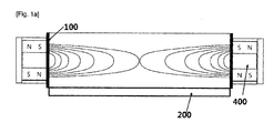
- FIG. 1a By looking Fig. 1a , there is the construction of plasma generation source of the present invention.
- More than one pair of belt type magnet(400) is mounted on the side wall of plasma chamber(100) that provides the space generating plasma, microwave irradiating equipment (200)(called launcher) is mounted on the upper side of the plasma chamber(100), microwave emits into plasma chamber(100) from the microwave irradiating equipment (200).
- the present invention from the microwave irradiating equipment (200), the place where microwave is incident into plasma chamber (100) is composed of complete opening without dielectric window so that it can solve the problem that penetration ratio would drop as contaminating window by deposition material during deposition process.
- Fig. 1b and Fig. 1c are sectional views about one pair of belt type magnet(400) mounted on outer wall of the plasma generating source on Fig. 1a . It means that A type of belt type magnet ( Fig. 1b ) and B type of belt type magnet ( Fig. 1c ) are arranged up and down and magnetic field such as the form of Fig. 1a can be formed. Such this belt type magnet can be arranged not just one pair but many pairs and due to this, inside of plasma generating space, magnetic field same curve line such as Fig. 1a is continuously distributed.
- Belt type magnet showed on Fig. 1b and Fig. 1c can be, of course, composed of circle type, elliptical track or any closed polygon type.
- the magnetic field continues without cutting and this is because of the consecutive construction of belt type magnet(400), and like this consecutive construction makes microwave incident through the opening of the top not the side wall of plasma chamber(100). Magnetic field which forms consecutively improves plasma confinement remarkably by collecting electrons of plasma that was generated and making them move on the trace of toroidal type and drift motion continuously along the side wall of plasma chamber. In other words, by looking electronic motion averagely, the consecutive trace of returning is shown like a cutting perspective view of Fig. 1d , so plasma deposition effect greatly can be improved.
- Plasma chamber (100) can be a cylinder type, a cylinder type that has circular or elliptical bottom or a faceted cylinder that has polygon bottom, the belt type magnet (400) is mounted on the side wall of plasma chamber(100), which is circle type, track, square or other various shapes depending the structure of plasma chamber(100) and forms Electron Cyclotron Resonance (ECR) magnetic field inside of plasma chamber(100).
- microwave irradiated from microwave irradiating equipment(200) can be used higher than plasma ion frequency, and plasma ion frequency is like following formula.
- ⁇ i 4 ⁇ ⁇ ⁇ n i ⁇ Z 2 ⁇ e 2 / m i
- n i ion density
- Z atom number
- e electron charge
- m i ion mass
- plasma generating source can increase plasma density, and magnetic field by more than one pair of belt type magnet(400) mounted to the outer wall and electric field of microwave irradiatied by microwave irradiating equipment
- ECR Electro Cyclotron Resonance
- microwave irradiating mode of microwave irradiating equipment (200) generating plasma can be controlled in pulse mode or continuous mode as necessary so that its applicability can be widen.
- microwave irradiating equipment (200) of Fig. 1a and Fig. 1d looks like circle type, elliptical type, track type or square type by using circle type and elliptical type.
- Fig. 2 shows that slit (250) is formed on microwave irradiating equipment (200) and Fig. 3 shows that slit is formed on toroidal type microwave irradiating equipment(200).
- Fig.4 shows square(rectangular) type or cylinder type microwave irradiating equipment (200). Like this, microwave irradiating equipment (200) can strengthen its emission power by composing plurality.
- Fig.5 shows sputtering system (800) that applied above plasma generating source.
- the sputtering system (800) can generate plasma by heating electron not affecting on plasma ion motion because microwave frequency is higher than plasma ion frequency.
- Bias voltage of the target (700,710,720) is applied lower frequency than plasma ion frequency so that it can control ion energy that is incident to the target, which is characterized in separating plasma generating power and ion acceleration voltage.
- Plasma generating power and ion accelerated voltage is dualized in the sputtering system (800) to maintain high density plasma stably regardless of target applied voltage, whereby it differentiates from conventional sputtering system by which is unstable at lower target applied voltage.
- conventional sputtering system has high target bias voltage so that it damages on thin film by generating high energy particles.
- the present sputtering equipment (800) can decrease target bias voltage to minimize the problems like the above, which is very advantageous.
- high density plasma can be uniformly distributed near target (720) thanks to the magnetic field structure of belt type magnet (400), etching distribution of the target becomes uniform so that it can increase usage efficiency of target (720).
- the target (720) can be composed of large area and it is because that plasma distribution can be formed high density across large area.
- bias voltage of target (700,710,720) on the present sputtering system (800) can be modified in various way such as D.C. voltage, alternating voltage, D.C. pulse, A.C. pulse or voltage combined with the above voltages depending on needs so that it is possible to control the character of thin film.
- the target (720) mounted parallel to the upper plate of the chamber and target (700, 710) mounted on the side wall of it are composed of different materials each other, so it is very convenient to be able to co-deposite host material and dopant at the same time.
- Zn from one target (700), In 2 O 3 from another target (710) and Ga 2 O 3 from the other target(720) can be formed, so IGZO can be formed on the substrate.
- IGZO can be formed on the substrate.
- it can minimize thin film damage at the same time by negative oxygen ion and also it has the merit of increasing deposition rate.
- Targets (700,710) mounted on the inner wall of plasma chamber can be composed of a plurality of target pieces to be arranged in radial directions.
- Target(720) arranged in plasma chamber as the way of horizontal plane can be mounted on upper plate of plasma chamber, or at the center of inside of chamber, and these can also be composed of many pieces.
- targets can be composed of many different materials, but it can be made of same material but adjusted their arrays for high speed, high efficiency, and uniform thin film deposition.
- the target composition such as large area target etc. is very free, and targets(700,710) mounted on the inner wall of plasma chamber is surrounded by magnetic field from belt type magnet (400) and high density plasma near target can be generated so that it is possible to get high efficiency sputtering.
- plasma chamber (100) is composed of a cylinder type with elliptical tract bottom or a faceted cylinder when a lot of targets (700,710) are installed in inner wall of like this plasma, it has the merits to be convenient to install many targets for reaching the optimum levels of numbers and percentage of components on thin film and to control magnetic field effect by belt type magnet (400) as well.
- sputtering system of this embodiment generates high density plasma at high vacuum and feature of straight on the particle sputtered is improved, and thin film aspect ratio with trench pattern can be improved.
- Sputtering system of this embodiment can control plasma generating power and ion accelerated voltage independently, and magnetic field formed by belt type magnet confine plasma charged particle, whereby it can minimize plasma-substrate interaction without extra plasma limiter so that it minimizes thin film damage by plasma.
- plasma limiters can be installed on the boundary of chamber as necessary, which is obvious to ordinary person of the technical field.
- Fig. 6 shows neutral particle beam source(900) structure modified from the above sputtering system (800).
- Neutral particle beam generating source (900) generates neutral particle beam of high flux on the same principle of above sputtering system
- Neutral particle beam generating source of this embodiment differentiates from conventional neutral particle beam generating source because it minimizes plasma-substrate interaction without plasma limiter.
- the advantage by increasing of mean free path shows in a same way with high flux of neutral particle beam on account of generating high density plasma under high vacuum.
- plasma limiters can be installed on the boundary of chamber as necessary, which is obvious to ordinary person of the technical field.
- Fig. 7 shows an embodiment of thin film deposition system (1000) made by combining the above sputtering system (800) and neutral particle beam generating source.
- thin film deposition system (1000) it has the merit of forming high quality thin film at low temperature process by providing necessary energy for thin film forming additionally due to neutral particle beam and by providing particle that consists of thin film due to sputtering system (800) at the same time.
- thin film deposition system(1000) is embodied by installing two of neutral particle beam generating source(900) one for each at both sides based on one sputtering system(800) at center.
- that combining method can be modified in various different ways by ordinary person of the technical field.
- one sputtering system (800) and one neutral particle beam generating source(900) can be combined.
- Fig. 8 shows the construction neutral particle generating source of the present invention further comprising limiter (500). Even though it minimizes plasma-substrate interaction without limiter, charged particles can be eliminated more completely when neutral particle beam emits from plasma chamber(100) into process chamber that has substrate(600) by further installing limiter(500).
- belt type magnet(400) can be constructed with not only permanent magnet but also electromagnet which can make microwave frequency increase, so plasma density can be improved.
- the present invention can be used widely in the process for forming the thin film using plasma, and it can use plasma generating source and thin film deposition system of the present invention in the field of advanced material especially, LED, solar battery, LED, diamond thin film etc.
Landscapes
- Chemical & Material Sciences (AREA)
- Engineering & Computer Science (AREA)
- Physics & Mathematics (AREA)
- Plasma & Fusion (AREA)
- Analytical Chemistry (AREA)
- Organic Chemistry (AREA)
- Mechanical Engineering (AREA)
- Metallurgy (AREA)
- Materials Engineering (AREA)
- Chemical Kinetics & Catalysis (AREA)
- Electromagnetism (AREA)
- Spectroscopy & Molecular Physics (AREA)
- Plasma Technology (AREA)
- Physical Vapour Deposition (AREA)
- Particle Accelerators (AREA)
- Electrodes Of Semiconductors (AREA)
Priority Applications (1)
| Application Number | Priority Date | Filing Date | Title |
|---|---|---|---|
| EP15191835.6A EP3002996B1 (de) | 2011-06-09 | 2012-06-01 | Neutrale teilchenstrahlquelle mit einem bandförmigen magneten und mikrowellen plasmaquelle |
Applications Claiming Priority (3)
| Application Number | Priority Date | Filing Date | Title |
|---|---|---|---|
| KR1020110055417A KR101307019B1 (ko) | 2011-06-09 | 2011-06-09 | 벨트형 자석을 포함한 중성입자 빔 발생장치 |
| KR1020120049386A KR101383530B1 (ko) | 2012-05-09 | 2012-05-09 | 벨트형 자석을 포함한 플라즈마 발생원 |
| PCT/KR2012/004345 WO2012169747A2 (ko) | 2011-06-09 | 2012-06-01 | 벨트형 자석을 포함한 플라즈마 발생원 및 이를 이용한 박막 증착 시스템 |
Related Child Applications (2)
| Application Number | Title | Priority Date | Filing Date |
|---|---|---|---|
| EP15191835.6A Division EP3002996B1 (de) | 2011-06-09 | 2012-06-01 | Neutrale teilchenstrahlquelle mit einem bandförmigen magneten und mikrowellen plasmaquelle |
| EP15191835.6A Division-Into EP3002996B1 (de) | 2011-06-09 | 2012-06-01 | Neutrale teilchenstrahlquelle mit einem bandförmigen magneten und mikrowellen plasmaquelle |
Publications (3)
| Publication Number | Publication Date |
|---|---|
| EP2720518A2 true EP2720518A2 (de) | 2014-04-16 |
| EP2720518A4 EP2720518A4 (de) | 2015-05-27 |
| EP2720518B1 EP2720518B1 (de) | 2016-12-28 |
Family
ID=47296564
Family Applications (2)
| Application Number | Title | Priority Date | Filing Date |
|---|---|---|---|
| EP15191835.6A Active EP3002996B1 (de) | 2011-06-09 | 2012-06-01 | Neutrale teilchenstrahlquelle mit einem bandförmigen magneten und mikrowellen plasmaquelle |
| EP12797155.4A Active EP2720518B1 (de) | 2011-06-09 | 2012-06-01 | Plasmaerzeugungsquelle mit einem bandförmigen magneten und dünnfilmabscheidungssystem damit |
Family Applications Before (1)
| Application Number | Title | Priority Date | Filing Date |
|---|---|---|---|
| EP15191835.6A Active EP3002996B1 (de) | 2011-06-09 | 2012-06-01 | Neutrale teilchenstrahlquelle mit einem bandförmigen magneten und mikrowellen plasmaquelle |
Country Status (5)
| Country | Link |
|---|---|
| US (1) | US9589772B2 (de) |
| EP (2) | EP3002996B1 (de) |
| JP (2) | JP5774778B2 (de) |
| CN (1) | CN103766002B (de) |
| WO (1) | WO2012169747A2 (de) |
Families Citing this family (111)
| Publication number | Priority date | Publication date | Assignee | Title |
|---|---|---|---|---|
| US9324576B2 (en) | 2010-05-27 | 2016-04-26 | Applied Materials, Inc. | Selective etch for silicon films |
| US10283321B2 (en) | 2011-01-18 | 2019-05-07 | Applied Materials, Inc. | Semiconductor processing system and methods using capacitively coupled plasma |
| US9064815B2 (en) | 2011-03-14 | 2015-06-23 | Applied Materials, Inc. | Methods for etch of metal and metal-oxide films |
| US8999856B2 (en) | 2011-03-14 | 2015-04-07 | Applied Materials, Inc. | Methods for etch of sin films |
| US9267739B2 (en) | 2012-07-18 | 2016-02-23 | Applied Materials, Inc. | Pedestal with multi-zone temperature control and multiple purge capabilities |
| US9373517B2 (en) | 2012-08-02 | 2016-06-21 | Applied Materials, Inc. | Semiconductor processing with DC assisted RF power for improved control |
| US9132436B2 (en) | 2012-09-21 | 2015-09-15 | Applied Materials, Inc. | Chemical control features in wafer process equipment |
| US10256079B2 (en) | 2013-02-08 | 2019-04-09 | Applied Materials, Inc. | Semiconductor processing systems having multiple plasma configurations |
| US9362130B2 (en) | 2013-03-01 | 2016-06-07 | Applied Materials, Inc. | Enhanced etching processes using remote plasma sources |
| US9040422B2 (en) | 2013-03-05 | 2015-05-26 | Applied Materials, Inc. | Selective titanium nitride removal |
| US20140271097A1 (en) | 2013-03-15 | 2014-09-18 | Applied Materials, Inc. | Processing systems and methods for halide scavenging |
| US9493879B2 (en) | 2013-07-12 | 2016-11-15 | Applied Materials, Inc. | Selective sputtering for pattern transfer |
| US9773648B2 (en) | 2013-08-30 | 2017-09-26 | Applied Materials, Inc. | Dual discharge modes operation for remote plasma |
| US20160282532A1 (en) * | 2013-10-30 | 2016-09-29 | Tecport Optics, Inc. | Ophthalmic optical filters for prevention and reduction of photophobic effects and responses |
| US9576809B2 (en) | 2013-11-04 | 2017-02-21 | Applied Materials, Inc. | Etch suppression with germanium |
| US9520303B2 (en) | 2013-11-12 | 2016-12-13 | Applied Materials, Inc. | Aluminum selective etch |
| US9245762B2 (en) | 2013-12-02 | 2016-01-26 | Applied Materials, Inc. | Procedure for etch rate consistency |
| US9499898B2 (en) | 2014-03-03 | 2016-11-22 | Applied Materials, Inc. | Layered thin film heater and method of fabrication |
| US9299537B2 (en) | 2014-03-20 | 2016-03-29 | Applied Materials, Inc. | Radial waveguide systems and methods for post-match control of microwaves |
| US9903020B2 (en) | 2014-03-31 | 2018-02-27 | Applied Materials, Inc. | Generation of compact alumina passivation layers on aluminum plasma equipment components |
| CN103985942B (zh) * | 2014-05-15 | 2016-03-30 | 南京航空航天大学 | 一种矩形波导到多米诺等离子波导转换器 |
| US9309598B2 (en) | 2014-05-28 | 2016-04-12 | Applied Materials, Inc. | Oxide and metal removal |
| US9496167B2 (en) | 2014-07-31 | 2016-11-15 | Applied Materials, Inc. | Integrated bit-line airgap formation and gate stack post clean |
| US9659753B2 (en) | 2014-08-07 | 2017-05-23 | Applied Materials, Inc. | Grooved insulator to reduce leakage current |
| US9553102B2 (en) | 2014-08-19 | 2017-01-24 | Applied Materials, Inc. | Tungsten separation |
| US9478434B2 (en) | 2014-09-24 | 2016-10-25 | Applied Materials, Inc. | Chlorine-based hardmask removal |
| US9613822B2 (en) | 2014-09-25 | 2017-04-04 | Applied Materials, Inc. | Oxide etch selectivity enhancement |
| US9966240B2 (en) | 2014-10-14 | 2018-05-08 | Applied Materials, Inc. | Systems and methods for internal surface conditioning assessment in plasma processing equipment |
| US9355922B2 (en) | 2014-10-14 | 2016-05-31 | Applied Materials, Inc. | Systems and methods for internal surface conditioning in plasma processing equipment |
| US11637002B2 (en) | 2014-11-26 | 2023-04-25 | Applied Materials, Inc. | Methods and systems to enhance process uniformity |
| US10573496B2 (en) * | 2014-12-09 | 2020-02-25 | Applied Materials, Inc. | Direct outlet toroidal plasma source |
| US10224210B2 (en) | 2014-12-09 | 2019-03-05 | Applied Materials, Inc. | Plasma processing system with direct outlet toroidal plasma source |
| CN104505326A (zh) * | 2014-12-19 | 2015-04-08 | 中国科学院嘉兴微电子仪器与设备工程中心 | 一种应用于等离子体设备的腔室结构及等离子体设备 |
| US9502258B2 (en) | 2014-12-23 | 2016-11-22 | Applied Materials, Inc. | Anisotropic gap etch |
| US11257693B2 (en) | 2015-01-09 | 2022-02-22 | Applied Materials, Inc. | Methods and systems to improve pedestal temperature control |
| US9728437B2 (en) | 2015-02-03 | 2017-08-08 | Applied Materials, Inc. | High temperature chuck for plasma processing systems |
| US20160225652A1 (en) | 2015-02-03 | 2016-08-04 | Applied Materials, Inc. | Low temperature chuck for plasma processing systems |
| US9881805B2 (en) | 2015-03-02 | 2018-01-30 | Applied Materials, Inc. | Silicon selective removal |
| US9691645B2 (en) | 2015-08-06 | 2017-06-27 | Applied Materials, Inc. | Bolted wafer chuck thermal management systems and methods for wafer processing systems |
| US9741593B2 (en) | 2015-08-06 | 2017-08-22 | Applied Materials, Inc. | Thermal management systems and methods for wafer processing systems |
| US9349605B1 (en) | 2015-08-07 | 2016-05-24 | Applied Materials, Inc. | Oxide etch selectivity systems and methods |
| CN105088195A (zh) * | 2015-08-26 | 2015-11-25 | 中国科学院等离子体物理研究所 | 一种快速自由基增强化学气相沉积薄膜的方法 |
| US10504700B2 (en) | 2015-08-27 | 2019-12-10 | Applied Materials, Inc. | Plasma etching systems and methods with secondary plasma injection |
| CN105369206A (zh) * | 2015-12-03 | 2016-03-02 | 凯盛光伏材料有限公司 | 一种制备柔性衬底薄膜的磁控溅射装置 |
| CN105483630A (zh) * | 2015-12-03 | 2016-04-13 | 凯盛光伏材料有限公司 | 一种制备柔性azo薄膜的方法 |
| US10504754B2 (en) | 2016-05-19 | 2019-12-10 | Applied Materials, Inc. | Systems and methods for improved semiconductor etching and component protection |
| US10522371B2 (en) | 2016-05-19 | 2019-12-31 | Applied Materials, Inc. | Systems and methods for improved semiconductor etching and component protection |
| US9865484B1 (en) | 2016-06-29 | 2018-01-09 | Applied Materials, Inc. | Selective etch using material modification and RF pulsing |
| US10062575B2 (en) | 2016-09-09 | 2018-08-28 | Applied Materials, Inc. | Poly directional etch by oxidation |
| US10629473B2 (en) | 2016-09-09 | 2020-04-21 | Applied Materials, Inc. | Footing removal for nitride spacer |
| US9721789B1 (en) | 2016-10-04 | 2017-08-01 | Applied Materials, Inc. | Saving ion-damaged spacers |
| US10062585B2 (en) | 2016-10-04 | 2018-08-28 | Applied Materials, Inc. | Oxygen compatible plasma source |
| US9934942B1 (en) | 2016-10-04 | 2018-04-03 | Applied Materials, Inc. | Chamber with flow-through source |
| US10546729B2 (en) | 2016-10-04 | 2020-01-28 | Applied Materials, Inc. | Dual-channel showerhead with improved profile |
| US10062579B2 (en) | 2016-10-07 | 2018-08-28 | Applied Materials, Inc. | Selective SiN lateral recess |
| US9947549B1 (en) | 2016-10-10 | 2018-04-17 | Applied Materials, Inc. | Cobalt-containing material removal |
| US9768034B1 (en) | 2016-11-11 | 2017-09-19 | Applied Materials, Inc. | Removal methods for high aspect ratio structures |
| US10163696B2 (en) | 2016-11-11 | 2018-12-25 | Applied Materials, Inc. | Selective cobalt removal for bottom up gapfill |
| US10242908B2 (en) | 2016-11-14 | 2019-03-26 | Applied Materials, Inc. | Airgap formation with damage-free copper |
| US10026621B2 (en) | 2016-11-14 | 2018-07-17 | Applied Materials, Inc. | SiN spacer profile patterning |
| US10566206B2 (en) | 2016-12-27 | 2020-02-18 | Applied Materials, Inc. | Systems and methods for anisotropic material breakthrough |
| US10431429B2 (en) | 2017-02-03 | 2019-10-01 | Applied Materials, Inc. | Systems and methods for radial and azimuthal control of plasma uniformity |
| US10403507B2 (en) | 2017-02-03 | 2019-09-03 | Applied Materials, Inc. | Shaped etch profile with oxidation |
| US10043684B1 (en) | 2017-02-06 | 2018-08-07 | Applied Materials, Inc. | Self-limiting atomic thermal etching systems and methods |
| US10319739B2 (en) | 2017-02-08 | 2019-06-11 | Applied Materials, Inc. | Accommodating imperfectly aligned memory holes |
| US10943834B2 (en) | 2017-03-13 | 2021-03-09 | Applied Materials, Inc. | Replacement contact process |
| US10319649B2 (en) | 2017-04-11 | 2019-06-11 | Applied Materials, Inc. | Optical emission spectroscopy (OES) for remote plasma monitoring |
| US11276559B2 (en) | 2017-05-17 | 2022-03-15 | Applied Materials, Inc. | Semiconductor processing chamber for multiple precursor flow |
| JP7176860B6 (ja) | 2017-05-17 | 2022-12-16 | アプライド マテリアルズ インコーポレイテッド | 前駆体の流れを改善する半導体処理チャンバ |
| US11276590B2 (en) | 2017-05-17 | 2022-03-15 | Applied Materials, Inc. | Multi-zone semiconductor substrate supports |
| US10497579B2 (en) | 2017-05-31 | 2019-12-03 | Applied Materials, Inc. | Water-free etching methods |
| US10049891B1 (en) | 2017-05-31 | 2018-08-14 | Applied Materials, Inc. | Selective in situ cobalt residue removal |
| US10920320B2 (en) | 2017-06-16 | 2021-02-16 | Applied Materials, Inc. | Plasma health determination in semiconductor substrate processing reactors |
| US10541246B2 (en) | 2017-06-26 | 2020-01-21 | Applied Materials, Inc. | 3D flash memory cells which discourage cross-cell electrical tunneling |
| US10727080B2 (en) | 2017-07-07 | 2020-07-28 | Applied Materials, Inc. | Tantalum-containing material removal |
| US10541184B2 (en) | 2017-07-11 | 2020-01-21 | Applied Materials, Inc. | Optical emission spectroscopic techniques for monitoring etching |
| US10354889B2 (en) | 2017-07-17 | 2019-07-16 | Applied Materials, Inc. | Non-halogen etching of silicon-containing materials |
| US10170336B1 (en) | 2017-08-04 | 2019-01-01 | Applied Materials, Inc. | Methods for anisotropic control of selective silicon removal |
| US10043674B1 (en) | 2017-08-04 | 2018-08-07 | Applied Materials, Inc. | Germanium etching systems and methods |
| US10297458B2 (en) | 2017-08-07 | 2019-05-21 | Applied Materials, Inc. | Process window widening using coated parts in plasma etch processes |
| US10283324B1 (en) | 2017-10-24 | 2019-05-07 | Applied Materials, Inc. | Oxygen treatment for nitride etching |
| US10128086B1 (en) | 2017-10-24 | 2018-11-13 | Applied Materials, Inc. | Silicon pretreatment for nitride removal |
| US10256112B1 (en) | 2017-12-08 | 2019-04-09 | Applied Materials, Inc. | Selective tungsten removal |
| US10903054B2 (en) | 2017-12-19 | 2021-01-26 | Applied Materials, Inc. | Multi-zone gas distribution systems and methods |
| US11328909B2 (en) | 2017-12-22 | 2022-05-10 | Applied Materials, Inc. | Chamber conditioning and removal processes |
| US10854426B2 (en) | 2018-01-08 | 2020-12-01 | Applied Materials, Inc. | Metal recess for semiconductor structures |
| US10964512B2 (en) | 2018-02-15 | 2021-03-30 | Applied Materials, Inc. | Semiconductor processing chamber multistage mixing apparatus and methods |
| US10679870B2 (en) | 2018-02-15 | 2020-06-09 | Applied Materials, Inc. | Semiconductor processing chamber multistage mixing apparatus |
| TWI766433B (zh) | 2018-02-28 | 2022-06-01 | 美商應用材料股份有限公司 | 形成氣隙的系統及方法 |
| US10593560B2 (en) | 2018-03-01 | 2020-03-17 | Applied Materials, Inc. | Magnetic induction plasma source for semiconductor processes and equipment |
| US10319600B1 (en) | 2018-03-12 | 2019-06-11 | Applied Materials, Inc. | Thermal silicon etch |
| US10497573B2 (en) | 2018-03-13 | 2019-12-03 | Applied Materials, Inc. | Selective atomic layer etching of semiconductor materials |
| US10573527B2 (en) | 2018-04-06 | 2020-02-25 | Applied Materials, Inc. | Gas-phase selective etching systems and methods |
| US10490406B2 (en) | 2018-04-10 | 2019-11-26 | Appled Materials, Inc. | Systems and methods for material breakthrough |
| US10699879B2 (en) | 2018-04-17 | 2020-06-30 | Applied Materials, Inc. | Two piece electrode assembly with gap for plasma control |
| US10886137B2 (en) | 2018-04-30 | 2021-01-05 | Applied Materials, Inc. | Selective nitride removal |
| US11037765B2 (en) * | 2018-07-03 | 2021-06-15 | Tokyo Electron Limited | Resonant structure for electron cyclotron resonant (ECR) plasma ionization |
| US10755941B2 (en) | 2018-07-06 | 2020-08-25 | Applied Materials, Inc. | Self-limiting selective etching systems and methods |
| US10872778B2 (en) | 2018-07-06 | 2020-12-22 | Applied Materials, Inc. | Systems and methods utilizing solid-phase etchants |
| US10672642B2 (en) | 2018-07-24 | 2020-06-02 | Applied Materials, Inc. | Systems and methods for pedestal configuration |
| US11049755B2 (en) | 2018-09-14 | 2021-06-29 | Applied Materials, Inc. | Semiconductor substrate supports with embedded RF shield |
| US10892198B2 (en) | 2018-09-14 | 2021-01-12 | Applied Materials, Inc. | Systems and methods for improved performance in semiconductor processing |
| US11062887B2 (en) | 2018-09-17 | 2021-07-13 | Applied Materials, Inc. | High temperature RF heater pedestals |
| US11417534B2 (en) | 2018-09-21 | 2022-08-16 | Applied Materials, Inc. | Selective material removal |
| US10714329B2 (en) * | 2018-09-28 | 2020-07-14 | Taiwan Semiconductor Manufacturing Co., Ltd. | Pre-clean for contacts |
| US11682560B2 (en) | 2018-10-11 | 2023-06-20 | Applied Materials, Inc. | Systems and methods for hafnium-containing film removal |
| US11121002B2 (en) | 2018-10-24 | 2021-09-14 | Applied Materials, Inc. | Systems and methods for etching metals and metal derivatives |
| US11437242B2 (en) | 2018-11-27 | 2022-09-06 | Applied Materials, Inc. | Selective removal of silicon-containing materials |
| US11721527B2 (en) | 2019-01-07 | 2023-08-08 | Applied Materials, Inc. | Processing chamber mixing systems |
| US10920319B2 (en) | 2019-01-11 | 2021-02-16 | Applied Materials, Inc. | Ceramic showerheads with conductive electrodes |
| CN113665848B (zh) * | 2021-08-27 | 2023-03-14 | 中国人民解放军国防科技大学 | 一种磁场力/力矩作用投送系统及其地面测试装置 |
Family Cites Families (27)
| Publication number | Priority date | Publication date | Assignee | Title |
|---|---|---|---|---|
| JPS6452062A (en) * | 1987-08-21 | 1989-02-28 | Nippon Telegraph & Telephone | Ionic source |
| US5022977A (en) * | 1986-09-29 | 1991-06-11 | Nippon Telegraph And Telephone Corporation | Ion generation apparatus and thin film forming apparatus and ion source utilizing the ion generation apparatus |
| JP2587924B2 (ja) * | 1986-10-11 | 1997-03-05 | 日本電信電話株式会社 | 薄膜形成装置 |
| EP0264913B1 (de) * | 1986-10-20 | 1994-06-22 | Hitachi, Ltd. | Plasmabearbeitungsgerät |
| KR880013424A (ko) | 1987-04-08 | 1988-11-30 | 미타 가츠시게 | 플라즈머 장치 |
| JP2561270B2 (ja) * | 1987-04-08 | 1996-12-04 | 株式会社日立製作所 | プラズマ装置 |
| KR920002864B1 (ko) * | 1987-07-20 | 1992-04-06 | 가부시기가이샤 히다찌세이사꾸쇼 | 플라즈마 처리방법 및 그 장치 |
| US5061838A (en) * | 1989-06-23 | 1991-10-29 | Massachusetts Institute Of Technology | Toroidal electron cyclotron resonance reactor |
| JP3020580B2 (ja) * | 1990-09-28 | 2000-03-15 | 株式会社日立製作所 | マイクロ波プラズマ処理装置 |
| US5359177A (en) * | 1990-11-14 | 1994-10-25 | Mitsubishi Denki Kabushiki Kaisha | Microwave plasma apparatus for generating a uniform plasma |
| JP3082331B2 (ja) * | 1991-08-01 | 2000-08-28 | 三菱電機株式会社 | 半導体製造装置および半導体装置の製造方法 |
| JPH07326495A (ja) * | 1994-05-30 | 1995-12-12 | Toshiba Corp | マイクロ波プラズマ発生装置 |
| JPH09125243A (ja) * | 1995-10-27 | 1997-05-13 | Canon Inc | 薄膜形成装置 |
| JPH09266096A (ja) * | 1996-03-28 | 1997-10-07 | Hitachi Ltd | プラズマ処理装置及びこれを用いたプラズマ処理方法 |
| JP4355036B2 (ja) * | 1997-03-18 | 2009-10-28 | キヤノンアネルバ株式会社 | イオン化スパッタリング装置 |
| JP3944946B2 (ja) * | 1997-04-25 | 2007-07-18 | 株式会社島津製作所 | 薄膜形成装置 |
| JPH11162956A (ja) | 1997-11-25 | 1999-06-18 | Hitachi Ltd | プラズマ処理装置 |
| US6610184B2 (en) | 2001-11-14 | 2003-08-26 | Applied Materials, Inc. | Magnet array in conjunction with rotating magnetron for plasma sputtering |
| US20030029716A1 (en) * | 2001-08-13 | 2003-02-13 | Ga-Lane Chen | DWDM filter system design |
| US7059268B2 (en) | 2002-12-20 | 2006-06-13 | Tokyo Electron Limited | Method, apparatus and magnet assembly for enhancing and localizing a capacitively coupled plasma |
| KR100555849B1 (ko) * | 2003-11-27 | 2006-03-03 | 주식회사 셈테크놀러지 | 중성입자빔 처리장치 |
| KR100714898B1 (ko) * | 2005-01-21 | 2007-05-04 | 삼성전자주식회사 | 중성빔을 이용한 기판 처리장치 및 처리방법 |
| KR100716258B1 (ko) * | 2006-06-29 | 2007-05-08 | 한국기초과학지원연구원 | 고체원소 중성입자빔 생성장치 및 방법 |
| KR100754370B1 (ko) | 2006-06-29 | 2007-09-03 | 한국기초과학지원연구원 | 향상된 중성입자 플럭스를 갖는 중성입자빔 생성장치 |
| EP2223328B1 (de) | 2007-12-07 | 2017-06-21 | Evatec AG | Verfahren zum magnetron-sputtern |
| KR101092906B1 (ko) * | 2009-06-11 | 2011-12-12 | 한국기초과학지원연구원 | 빔 플럭스 및 수송효율이 향상된 중성입자빔 생성장치 및 생성 방법 |
| WO2011025143A2 (ko) * | 2009-08-24 | 2011-03-03 | 한국기초과학지원연구원 | 플라즈마 발생용 마이크로웨이브 안테나 |
-
2012
- 2012-06-01 CN CN201280026487.XA patent/CN103766002B/zh active Active
- 2012-06-01 US US14/124,571 patent/US9589772B2/en active Active
- 2012-06-01 WO PCT/KR2012/004345 patent/WO2012169747A2/ko not_active Ceased
- 2012-06-01 EP EP15191835.6A patent/EP3002996B1/de active Active
- 2012-06-01 JP JP2014513443A patent/JP5774778B2/ja active Active
- 2012-06-01 EP EP12797155.4A patent/EP2720518B1/de active Active
-
2014
- 2014-12-24 JP JP2014259691A patent/JP6006286B2/ja active Active
Also Published As
| Publication number | Publication date |
|---|---|
| US9589772B2 (en) | 2017-03-07 |
| WO2012169747A2 (ko) | 2012-12-13 |
| JP2015133321A (ja) | 2015-07-23 |
| EP3002996B1 (de) | 2020-03-25 |
| JP2014522551A (ja) | 2014-09-04 |
| JP6006286B2 (ja) | 2016-10-12 |
| CN103766002A (zh) | 2014-04-30 |
| CN103766002B (zh) | 2017-03-22 |
| JP5774778B2 (ja) | 2015-09-09 |
| EP2720518A4 (de) | 2015-05-27 |
| WO2012169747A3 (ko) | 2013-03-28 |
| US20140124364A1 (en) | 2014-05-08 |
| EP2720518B1 (de) | 2016-12-28 |
| EP3002996A1 (de) | 2016-04-06 |
Similar Documents
| Publication | Publication Date | Title |
|---|---|---|
| US9589772B2 (en) | Plasma generation source including belt-type magnet and thin film deposition system using this | |
| Gudmundsson | Physics and technology of magnetron sputtering discharges | |
| Okumura | Inductively coupled plasma sources and applications | |
| US8728588B2 (en) | Method of treating a surface of at least one part by means of individual sources of an electron cyclotron resonance plasma | |
| JP2021502688A (ja) | 線形化されたエネルギーの無線周波数プラズマイオン供給源 | |
| CN104507250B (zh) | 一种等离子体光子晶体的产生装置 | |
| KR20150105181A (ko) | 자기 제한을 갖는 플라즈마 소스를 이용하는 플라즈마 기반 재료 변경 | |
| CN105887026B (zh) | 物理气相沉积系统与应用其的物理气相沉积方法 | |
| US10861667B2 (en) | Methods and systems for plasma deposition and treatment | |
| US20120001550A1 (en) | Magnetic modue of electron cyclotron resonance and electron cyclotron resonance apparatus using the same | |
| CN112292475B (zh) | 具有多阴极的沉积系统 | |
| TWI471894B (zh) | A plasma generating source including a ribbon magnet, and a thin film deposition system using the same | |
| US20260004990A1 (en) | Linear tcp source, a charged particle beam source using the linear tcp source and a grid for the charged particle beam source | |
| CN107447195B (zh) | 磁控管及磁控溅射系统 | |
| Gordon | Low-energy ion beamline-scattering apparatus with application to charge exchange collisions at surfaces | |
| KR101383530B1 (ko) | 벨트형 자석을 포함한 플라즈마 발생원 | |
| KR20140031355A (ko) | 벨트형 자석을 포함한 플라즈마 발생원 | |
| KR101307019B1 (ko) | 벨트형 자석을 포함한 중성입자 빔 발생장치 | |
| KR101305588B1 (ko) | 중성자 발생원 | |
| CN114318259A (zh) | 溅射沉积设备及方法 | |
| US20240021421A1 (en) | Vacuum deposition into trenches and vias | |
| Stamate | 3D Plasma-sheath-lenses: phenomenology and applications | |
| McLain | Linear magnetron high deposition rate magnet pack for high power impulse magnetron sputtering | |
| Ipanaque | Analysis and Simulations of Cold Plasmas Generated by Magnetron Sputtering | |
| US9865436B1 (en) | Powered anode for ion source for DLC and reactive processes |
Legal Events
| Date | Code | Title | Description |
|---|---|---|---|
| PUAI | Public reference made under article 153(3) epc to a published international application that has entered the european phase |
Free format text: ORIGINAL CODE: 0009012 |
|
| 17P | Request for examination filed |
Effective date: 20131203 |
|
| AK | Designated contracting states |
Kind code of ref document: A2 Designated state(s): AL AT BE BG CH CY CZ DE DK EE ES FI FR GB GR HR HU IE IS IT LI LT LU LV MC MK MT NL NO PL PT RO RS SE SI SK SM TR |
|
| DAX | Request for extension of the european patent (deleted) | ||
| RIC1 | Information provided on ipc code assigned before grant |
Ipc: H05H 1/34 20060101AFI20141211BHEP Ipc: H01J 37/32 20060101ALI20141211BHEP Ipc: H01L 21/205 20060101ALI20141211BHEP Ipc: C23C 16/50 20060101ALI20141211BHEP |
|
| REG | Reference to a national code |
Ref country code: DE Ref legal event code: R079 Ref document number: 602012027167 Country of ref document: DE Free format text: PREVIOUS MAIN CLASS: H05H0001340000 Ipc: H05H0001460000 |
|
| A4 | Supplementary search report drawn up and despatched |
Effective date: 20150428 |
|
| RIC1 | Information provided on ipc code assigned before grant |
Ipc: H01L 21/205 20060101ALI20150421BHEP Ipc: H05H 1/46 20060101AFI20150421BHEP Ipc: H01J 37/32 20060101ALI20150421BHEP Ipc: C23C 16/50 20060101ALI20150421BHEP Ipc: H01J 37/34 20060101ALI20150421BHEP |
|
| 17Q | First examination report despatched |
Effective date: 20160201 |
|
| GRAP | Despatch of communication of intention to grant a patent |
Free format text: ORIGINAL CODE: EPIDOSNIGR1 |
|
| INTG | Intention to grant announced |
Effective date: 20160915 |
|
| GRAS | Grant fee paid |
Free format text: ORIGINAL CODE: EPIDOSNIGR3 |
|
| GRAA | (expected) grant |
Free format text: ORIGINAL CODE: 0009210 |
|
| AK | Designated contracting states |
Kind code of ref document: B1 Designated state(s): AL AT BE BG CH CY CZ DE DK EE ES FI FR GB GR HR HU IE IS IT LI LT LU LV MC MK MT NL NO PL PT RO RS SE SI SK SM TR |
|
| REG | Reference to a national code |
Ref country code: GB Ref legal event code: FG4D |
|
| REG | Reference to a national code |
Ref country code: CH Ref legal event code: EP |
|
| REG | Reference to a national code |
Ref country code: AT Ref legal event code: REF Ref document number: 858269 Country of ref document: AT Kind code of ref document: T Effective date: 20170115 |
|
| REG | Reference to a national code |
Ref country code: IE Ref legal event code: FG4D |
|
| REG | Reference to a national code |
Ref country code: DE Ref legal event code: R096 Ref document number: 602012027167 Country of ref document: DE |
|
| PG25 | Lapsed in a contracting state [announced via postgrant information from national office to epo] |
Ref country code: LV Free format text: LAPSE BECAUSE OF FAILURE TO SUBMIT A TRANSLATION OF THE DESCRIPTION OR TO PAY THE FEE WITHIN THE PRESCRIBED TIME-LIMIT Effective date: 20161228 |
|
| REG | Reference to a national code |
Ref country code: LT Ref legal event code: MG4D |
|
| PG25 | Lapsed in a contracting state [announced via postgrant information from national office to epo] |
Ref country code: SE Free format text: LAPSE BECAUSE OF FAILURE TO SUBMIT A TRANSLATION OF THE DESCRIPTION OR TO PAY THE FEE WITHIN THE PRESCRIBED TIME-LIMIT Effective date: 20161228 Ref country code: NO Free format text: LAPSE BECAUSE OF FAILURE TO SUBMIT A TRANSLATION OF THE DESCRIPTION OR TO PAY THE FEE WITHIN THE PRESCRIBED TIME-LIMIT Effective date: 20170328 Ref country code: GR Free format text: LAPSE BECAUSE OF FAILURE TO SUBMIT A TRANSLATION OF THE DESCRIPTION OR TO PAY THE FEE WITHIN THE PRESCRIBED TIME-LIMIT Effective date: 20170329 Ref country code: LT Free format text: LAPSE BECAUSE OF FAILURE TO SUBMIT A TRANSLATION OF THE DESCRIPTION OR TO PAY THE FEE WITHIN THE PRESCRIBED TIME-LIMIT Effective date: 20161228 |
|
| REG | Reference to a national code |
Ref country code: NL Ref legal event code: MP Effective date: 20161228 |
|
| REG | Reference to a national code |
Ref country code: AT Ref legal event code: MK05 Ref document number: 858269 Country of ref document: AT Kind code of ref document: T Effective date: 20161228 |
|
| REG | Reference to a national code |
Ref country code: FR Ref legal event code: PLFP Year of fee payment: 6 |
|
| PG25 | Lapsed in a contracting state [announced via postgrant information from national office to epo] |
Ref country code: FI Free format text: LAPSE BECAUSE OF FAILURE TO SUBMIT A TRANSLATION OF THE DESCRIPTION OR TO PAY THE FEE WITHIN THE PRESCRIBED TIME-LIMIT Effective date: 20161228 Ref country code: RS Free format text: LAPSE BECAUSE OF FAILURE TO SUBMIT A TRANSLATION OF THE DESCRIPTION OR TO PAY THE FEE WITHIN THE PRESCRIBED TIME-LIMIT Effective date: 20161228 Ref country code: HR Free format text: LAPSE BECAUSE OF FAILURE TO SUBMIT A TRANSLATION OF THE DESCRIPTION OR TO PAY THE FEE WITHIN THE PRESCRIBED TIME-LIMIT Effective date: 20161228 |
|
| PG25 | Lapsed in a contracting state [announced via postgrant information from national office to epo] |
Ref country code: NL Free format text: LAPSE BECAUSE OF FAILURE TO SUBMIT A TRANSLATION OF THE DESCRIPTION OR TO PAY THE FEE WITHIN THE PRESCRIBED TIME-LIMIT Effective date: 20161228 |
|
| PG25 | Lapsed in a contracting state [announced via postgrant information from national office to epo] |
Ref country code: EE Free format text: LAPSE BECAUSE OF FAILURE TO SUBMIT A TRANSLATION OF THE DESCRIPTION OR TO PAY THE FEE WITHIN THE PRESCRIBED TIME-LIMIT Effective date: 20161228 Ref country code: IS Free format text: LAPSE BECAUSE OF FAILURE TO SUBMIT A TRANSLATION OF THE DESCRIPTION OR TO PAY THE FEE WITHIN THE PRESCRIBED TIME-LIMIT Effective date: 20170428 Ref country code: SK Free format text: LAPSE BECAUSE OF FAILURE TO SUBMIT A TRANSLATION OF THE DESCRIPTION OR TO PAY THE FEE WITHIN THE PRESCRIBED TIME-LIMIT Effective date: 20161228 Ref country code: RO Free format text: LAPSE BECAUSE OF FAILURE TO SUBMIT A TRANSLATION OF THE DESCRIPTION OR TO PAY THE FEE WITHIN THE PRESCRIBED TIME-LIMIT Effective date: 20161228 Ref country code: CZ Free format text: LAPSE BECAUSE OF FAILURE TO SUBMIT A TRANSLATION OF THE DESCRIPTION OR TO PAY THE FEE WITHIN THE PRESCRIBED TIME-LIMIT Effective date: 20161228 |
|
| PG25 | Lapsed in a contracting state [announced via postgrant information from national office to epo] |
Ref country code: PL Free format text: LAPSE BECAUSE OF FAILURE TO SUBMIT A TRANSLATION OF THE DESCRIPTION OR TO PAY THE FEE WITHIN THE PRESCRIBED TIME-LIMIT Effective date: 20161228 Ref country code: ES Free format text: LAPSE BECAUSE OF FAILURE TO SUBMIT A TRANSLATION OF THE DESCRIPTION OR TO PAY THE FEE WITHIN THE PRESCRIBED TIME-LIMIT Effective date: 20161228 Ref country code: BG Free format text: LAPSE BECAUSE OF FAILURE TO SUBMIT A TRANSLATION OF THE DESCRIPTION OR TO PAY THE FEE WITHIN THE PRESCRIBED TIME-LIMIT Effective date: 20170328 Ref country code: PT Free format text: LAPSE BECAUSE OF FAILURE TO SUBMIT A TRANSLATION OF THE DESCRIPTION OR TO PAY THE FEE WITHIN THE PRESCRIBED TIME-LIMIT Effective date: 20170428 Ref country code: SM Free format text: LAPSE BECAUSE OF FAILURE TO SUBMIT A TRANSLATION OF THE DESCRIPTION OR TO PAY THE FEE WITHIN THE PRESCRIBED TIME-LIMIT Effective date: 20161228 Ref country code: AT Free format text: LAPSE BECAUSE OF FAILURE TO SUBMIT A TRANSLATION OF THE DESCRIPTION OR TO PAY THE FEE WITHIN THE PRESCRIBED TIME-LIMIT Effective date: 20161228 Ref country code: BE Free format text: LAPSE BECAUSE OF FAILURE TO SUBMIT A TRANSLATION OF THE DESCRIPTION OR TO PAY THE FEE WITHIN THE PRESCRIBED TIME-LIMIT Effective date: 20161228 |
|
| REG | Reference to a national code |
Ref country code: DE Ref legal event code: R097 Ref document number: 602012027167 Country of ref document: DE |
|
| PLBE | No opposition filed within time limit |
Free format text: ORIGINAL CODE: 0009261 |
|
| STAA | Information on the status of an ep patent application or granted ep patent |
Free format text: STATUS: NO OPPOSITION FILED WITHIN TIME LIMIT |
|
| PG25 | Lapsed in a contracting state [announced via postgrant information from national office to epo] |
Ref country code: DK Free format text: LAPSE BECAUSE OF FAILURE TO SUBMIT A TRANSLATION OF THE DESCRIPTION OR TO PAY THE FEE WITHIN THE PRESCRIBED TIME-LIMIT Effective date: 20161228 |
|
| 26N | No opposition filed |
Effective date: 20170929 |
|
| PG25 | Lapsed in a contracting state [announced via postgrant information from national office to epo] |
Ref country code: MC Free format text: LAPSE BECAUSE OF FAILURE TO SUBMIT A TRANSLATION OF THE DESCRIPTION OR TO PAY THE FEE WITHIN THE PRESCRIBED TIME-LIMIT Effective date: 20161228 |
|
| REG | Reference to a national code |
Ref country code: CH Ref legal event code: PL |
|
| PG25 | Lapsed in a contracting state [announced via postgrant information from national office to epo] |
Ref country code: SI Free format text: LAPSE BECAUSE OF FAILURE TO SUBMIT A TRANSLATION OF THE DESCRIPTION OR TO PAY THE FEE WITHIN THE PRESCRIBED TIME-LIMIT Effective date: 20161228 |
|
| REG | Reference to a national code |
Ref country code: IE Ref legal event code: MM4A |
|
| REG | Reference to a national code |
Ref country code: FR Ref legal event code: PLFP Year of fee payment: 7 |
|
| PG25 | Lapsed in a contracting state [announced via postgrant information from national office to epo] |
Ref country code: LU Free format text: LAPSE BECAUSE OF NON-PAYMENT OF DUE FEES Effective date: 20170601 Ref country code: LI Free format text: LAPSE BECAUSE OF NON-PAYMENT OF DUE FEES Effective date: 20170630 Ref country code: CH Free format text: LAPSE BECAUSE OF NON-PAYMENT OF DUE FEES Effective date: 20170630 Ref country code: IE Free format text: LAPSE BECAUSE OF NON-PAYMENT OF DUE FEES Effective date: 20170601 |
|
| PG25 | Lapsed in a contracting state [announced via postgrant information from national office to epo] |
Ref country code: MT Free format text: LAPSE BECAUSE OF NON-PAYMENT OF DUE FEES Effective date: 20170601 |
|
| PG25 | Lapsed in a contracting state [announced via postgrant information from national office to epo] |
Ref country code: HU Free format text: LAPSE BECAUSE OF FAILURE TO SUBMIT A TRANSLATION OF THE DESCRIPTION OR TO PAY THE FEE WITHIN THE PRESCRIBED TIME-LIMIT; INVALID AB INITIO Effective date: 20120601 |
|
| PG25 | Lapsed in a contracting state [announced via postgrant information from national office to epo] |
Ref country code: CY Free format text: LAPSE BECAUSE OF NON-PAYMENT OF DUE FEES Effective date: 20161228 |
|
| PG25 | Lapsed in a contracting state [announced via postgrant information from national office to epo] |
Ref country code: MK Free format text: LAPSE BECAUSE OF FAILURE TO SUBMIT A TRANSLATION OF THE DESCRIPTION OR TO PAY THE FEE WITHIN THE PRESCRIBED TIME-LIMIT Effective date: 20161228 |
|
| PG25 | Lapsed in a contracting state [announced via postgrant information from national office to epo] |
Ref country code: TR Free format text: LAPSE BECAUSE OF FAILURE TO SUBMIT A TRANSLATION OF THE DESCRIPTION OR TO PAY THE FEE WITHIN THE PRESCRIBED TIME-LIMIT Effective date: 20161228 |
|
| PG25 | Lapsed in a contracting state [announced via postgrant information from national office to epo] |
Ref country code: AL Free format text: LAPSE BECAUSE OF FAILURE TO SUBMIT A TRANSLATION OF THE DESCRIPTION OR TO PAY THE FEE WITHIN THE PRESCRIBED TIME-LIMIT Effective date: 20161228 |
|
| REG | Reference to a national code |
Ref country code: DE Ref legal event code: R082 Ref document number: 602012027167 Country of ref document: DE Representative=s name: BETTEN & RESCH PATENT- UND RECHTSANWAELTE PART, DE Ref country code: DE Ref legal event code: R081 Ref document number: 602012027167 Country of ref document: DE Owner name: KOREA INSTITUTE OF FUSION ENERGY, YUSEONG-GU, KR Free format text: FORMER OWNER: KOREA BASIC SCIENCE INSTITUTE, DAEJEON, KR |
|
| REG | Reference to a national code |
Ref country code: GB Ref legal event code: 732E Free format text: REGISTERED BETWEEN 20210708 AND 20210714 |
|
| PGFP | Annual fee paid to national office [announced via postgrant information from national office to epo] |
Ref country code: IT Payment date: 20250321 Year of fee payment: 14 |
|
| PGFP | Annual fee paid to national office [announced via postgrant information from national office to epo] |
Ref country code: DE Payment date: 20250320 Year of fee payment: 14 |
|
| PGFP | Annual fee paid to national office [announced via postgrant information from national office to epo] |
Ref country code: GB Payment date: 20250407 Year of fee payment: 14 |
|
| PGFP | Annual fee paid to national office [announced via postgrant information from national office to epo] |
Ref country code: FR Payment date: 20260323 Year of fee payment: 15 |