EP2722734A2 - Electrode filaire pour panneau à écran tactile - Google Patents
Electrode filaire pour panneau à écran tactile Download PDFInfo
- Publication number
- EP2722734A2 EP2722734A2 EP12800960.2A EP12800960A EP2722734A2 EP 2722734 A2 EP2722734 A2 EP 2722734A2 EP 12800960 A EP12800960 A EP 12800960A EP 2722734 A2 EP2722734 A2 EP 2722734A2
- Authority
- EP
- European Patent Office
- Prior art keywords
- wired electrode
- touch screen
- groove
- screen panel
- signal transmitting
- Prior art date
- Legal status (The legal status is an assumption and is not a legal conclusion. Google has not performed a legal analysis and makes no representation as to the accuracy of the status listed.)
- Granted
Links
Images


Classifications
-
- G—PHYSICS
- G06—COMPUTING OR CALCULATING; COUNTING
- G06F—ELECTRIC DIGITAL DATA PROCESSING
- G06F3/00—Input arrangements for transferring data to be processed into a form capable of being handled by the computer; Output arrangements for transferring data from processing unit to output unit, e.g. interface arrangements
- G06F3/01—Input arrangements or combined input and output arrangements for interaction between user and computer
- G06F3/03—Arrangements for converting the position or the displacement of a member into a coded form
- G06F3/041—Digitisers, e.g. for touch screens or touch pads, characterised by the transducing means
-
- G—PHYSICS
- G06—COMPUTING OR CALCULATING; COUNTING
- G06F—ELECTRIC DIGITAL DATA PROCESSING
- G06F3/00—Input arrangements for transferring data to be processed into a form capable of being handled by the computer; Output arrangements for transferring data from processing unit to output unit, e.g. interface arrangements
- G06F3/01—Input arrangements or combined input and output arrangements for interaction between user and computer
- G06F3/03—Arrangements for converting the position or the displacement of a member into a coded form
- G06F3/041—Digitisers, e.g. for touch screens or touch pads, characterised by the transducing means
- G06F3/0416—Control or interface arrangements specially adapted for digitisers
- G06F3/04164—Connections between sensors and controllers, e.g. routing lines between electrodes and connection pads
-
- G—PHYSICS
- G06—COMPUTING OR CALCULATING; COUNTING
- G06F—ELECTRIC DIGITAL DATA PROCESSING
- G06F3/00—Input arrangements for transferring data to be processed into a form capable of being handled by the computer; Output arrangements for transferring data from processing unit to output unit, e.g. interface arrangements
- G06F3/01—Input arrangements or combined input and output arrangements for interaction between user and computer
- G06F3/03—Arrangements for converting the position or the displacement of a member into a coded form
- G06F3/041—Digitisers, e.g. for touch screens or touch pads, characterised by the transducing means
- G06F3/044—Digitisers, e.g. for touch screens or touch pads, characterised by the transducing means by capacitive means
-
- G—PHYSICS
- G06—COMPUTING OR CALCULATING; COUNTING
- G06F—ELECTRIC DIGITAL DATA PROCESSING
- G06F3/00—Input arrangements for transferring data to be processed into a form capable of being handled by the computer; Output arrangements for transferring data from processing unit to output unit, e.g. interface arrangements
- G06F3/01—Input arrangements or combined input and output arrangements for interaction between user and computer
- G06F3/03—Arrangements for converting the position or the displacement of a member into a coded form
- G06F3/041—Digitisers, e.g. for touch screens or touch pads, characterised by the transducing means
- G06F3/044—Digitisers, e.g. for touch screens or touch pads, characterised by the transducing means by capacitive means
- G06F3/0446—Digitisers, e.g. for touch screens or touch pads, characterised by the transducing means by capacitive means using a grid-like structure of electrodes in at least two directions, e.g. using row and column electrodes
-
- G—PHYSICS
- G06—COMPUTING OR CALCULATING; COUNTING
- G06F—ELECTRIC DIGITAL DATA PROCESSING
- G06F3/00—Input arrangements for transferring data to be processed into a form capable of being handled by the computer; Output arrangements for transferring data from processing unit to output unit, e.g. interface arrangements
- G06F3/01—Input arrangements or combined input and output arrangements for interaction between user and computer
- G06F3/03—Arrangements for converting the position or the displacement of a member into a coded form
- G06F3/041—Digitisers, e.g. for touch screens or touch pads, characterised by the transducing means
- G06F3/046—Digitisers, e.g. for touch screens or touch pads, characterised by the transducing means by electromagnetic means
-
- H—ELECTRICITY
- H05—ELECTRIC TECHNIQUES NOT OTHERWISE PROVIDED FOR
- H05K—PRINTED CIRCUITS; CASINGS OR CONSTRUCTIONAL DETAILS OF ELECTRIC APPARATUS; MANUFACTURE OF ASSEMBLAGES OF ELECTRICAL COMPONENTS
- H05K1/00—Printed circuits
- H05K1/02—Details
- H05K1/0296—Conductive pattern lay-out details not covered by sub groups H05K1/02 - H05K1/0295
-
- H—ELECTRICITY
- H05—ELECTRIC TECHNIQUES NOT OTHERWISE PROVIDED FOR
- H05K—PRINTED CIRCUITS; CASINGS OR CONSTRUCTIONAL DETAILS OF ELECTRIC APPARATUS; MANUFACTURE OF ASSEMBLAGES OF ELECTRICAL COMPONENTS
- H05K3/00—Apparatus or processes for manufacturing printed circuits
- H05K3/10—Apparatus or processes for manufacturing printed circuits in which conductive material is applied to the insulating support in such a manner as to form the desired conductive pattern
- H05K3/12—Apparatus or processes for manufacturing printed circuits in which conductive material is applied to the insulating support in such a manner as to form the desired conductive pattern using thick film techniques, e.g. printing techniques to apply the conductive material or similar techniques for applying conductive paste or ink patterns
- H05K3/1258—Apparatus or processes for manufacturing printed circuits in which conductive material is applied to the insulating support in such a manner as to form the desired conductive pattern using thick film techniques, e.g. printing techniques to apply the conductive material or similar techniques for applying conductive paste or ink patterns by using a substrate provided with a shape pattern, e.g. grooves, banks, resist pattern
-
- G—PHYSICS
- G06—COMPUTING OR CALCULATING; COUNTING
- G06F—ELECTRIC DIGITAL DATA PROCESSING
- G06F2203/00—Indexing scheme relating to G06F3/00 - G06F3/048
- G06F2203/041—Indexing scheme relating to G06F3/041 - G06F3/045
- G06F2203/04103—Manufacturing, i.e. details related to manufacturing processes specially suited for touch sensitive devices
-
- H—ELECTRICITY
- H05—ELECTRIC TECHNIQUES NOT OTHERWISE PROVIDED FOR
- H05K—PRINTED CIRCUITS; CASINGS OR CONSTRUCTIONAL DETAILS OF ELECTRIC APPARATUS; MANUFACTURE OF ASSEMBLAGES OF ELECTRICAL COMPONENTS
- H05K2201/00—Indexing scheme relating to printed circuits covered by H05K1/00
- H05K2201/09—Shape and layout
- H05K2201/09009—Substrate related
- H05K2201/09036—Recesses or grooves in insulating substrate
-
- H—ELECTRICITY
- H05—ELECTRIC TECHNIQUES NOT OTHERWISE PROVIDED FOR
- H05K—PRINTED CIRCUITS; CASINGS OR CONSTRUCTIONAL DETAILS OF ELECTRIC APPARATUS; MANUFACTURE OF ASSEMBLAGES OF ELECTRICAL COMPONENTS
- H05K2201/00—Indexing scheme relating to printed circuits covered by H05K1/00
- H05K2201/09—Shape and layout
- H05K2201/09009—Substrate related
- H05K2201/09045—Locally raised area or protrusion of insulating substrate
-
- H—ELECTRICITY
- H05—ELECTRIC TECHNIQUES NOT OTHERWISE PROVIDED FOR
- H05K—PRINTED CIRCUITS; CASINGS OR CONSTRUCTIONAL DETAILS OF ELECTRIC APPARATUS; MANUFACTURE OF ASSEMBLAGES OF ELECTRICAL COMPONENTS
- H05K2203/00—Indexing scheme relating to apparatus or processes for manufacturing printed circuits covered by H05K3/00
- H05K2203/01—Tools for processing; Objects used during processing
- H05K2203/0104—Tools for processing; Objects used during processing for patterning or coating
- H05K2203/0108—Male die used for patterning, punching or transferring
Definitions
- the present invention relates to a wired electrode of touch screen panel, and more particularly, to a wired electrode for transmitting a touch signal sensed by a signal sensing pattern of a touch screen panel to an external driving circuit, wherein the wired electrode includes curved portions or fine protrusions.
- a touch screen panel is an input device that allows a user to input commands by selecting instruction contents on a screen of an image display device through the use of hand or object.
- the touch screen panel is provided on a front face of the image display device, wherein the touch screen panel converts a contact location being in direct contact with the user's hand or object into electrical signals.
- the instruction contents selected at the contact location may be accepted as an input signal.
- the touch screen panel can replace a separate input device, which is operated while being connected with the image display device, for example, keyboard and mouse, whereby an application field of the touch screen panel expands gradually.
- a method for realizing the touch screen panel may be classified into a resistive type, capacitive type, and electro-magnetic type.
- resistive type capacitive type
- electro-magnetic type two of the most typical types may be the resistive type and capacitive type.
- the touch screen panel of resistive type is formed of two substrates coated with transparent electrode.
- the touch screen panel of resistive type is touched (or pressed) by the use of finger or pen, corresponding portions of the two substrates being at the touch point are attached to each other, to thereby detect the location of the touch.
- an application field of the resistive type has been reduced due to disadvantages such as difficulty of operation and inaccuracy in detecting the location of the touch.
- a signal sensing pattern senses a change of capacitance by other signal sensing patterns or grounding electrode, whereby the location of the touch is changed into an electrical signal. That is, it uses a principle of sensing static electricity of human body.
- This capacitive type touch screen panel has good durability, good transmittance, and rapid response time. Recently, the capacitive type touch screen panel has been widely used.
- the signal sensing patterns for sensing the location of the touch for example, a location touched by a user's finger occupy the most of screen; and a wired electrode for transmitting the touch signal sensed by the signal sensing patterns to an external driving circuit for driving electronic equipment with the touch screen panel is positioned in the margin of screen.
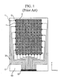
- FIG. 1 illustrates a wired electrode of touch screen panel according to the related art.
- the related art touch screen panel includes signal sensing patterns 1 and 2 for sensing a user's touch signal, and wired electrodes 10, 30 and 50 for transmitting the sensed touch signal to an external driving circuit (not shown), wherein the signal sensing patterns 1 and 2 are provided in the center of substrate 100.
- the wired electrodes are formed of a contact part 10 connected with the signal sensing patterns 1 and 2, a bonding part 50 electrically connected with the external driving circuit, and a signal transmitting part 30 for connecting the contact part 10 and bonding part 50 with each other.
- the wired electrodes enable to transmit electrical signals by forming a groove in the substrate 100 and filling the groove with a conductive material.
- a demolding process is carried out by the use of embossing mold whose shape corresponds to the groove.
- the signal transmitting part 30 of the wired electrode is provided with a folded portion 11.
- an embossing portion corresponding to the folded portion 11 is provided in the embossing mold for the demolding process. This embossing portion of the mold may be broken during the demolding process.
- the wired electrode is formed by filling the simple-shaped groove with the conductive material, the filled conductive material may be easily separated during a process for manufacturing the touch screen panel. In this case, the touch signal sensed by the signal sensing patterns 1 and 2 is not transmitted to the external driving circuit.
- the present invention has been made in view of the above problems, and it is an object of the present invention to provide a wired electrode of touch screen panel, which prevents an embossing mold for forming a wired electrode of a groove in a resin layer deposited on a substrate of touch screen panel from being broken for a demolding process, and obtains filling stability when the groove is filled with a conductive material by the use of doctor blade.
- Another object of the present invention is to provide a wired electrode including a plurality of fine protrusions to prevent a conductive material from being separated from a groove of a substrate for forming the wired electrode of touch screen panel.
- a wired electrode of a touch screen panel for transmitting a touch signal sensed by a signal sensing pattern of the touch screen panel to an external driving circuit, the wired electrode formed on a substrate and comprising at least one curved portion.
- the wired electrode may comprise a conductive material in a groove of a resin layer on the substrate.
- a plurality of fine protrusions may be formed on an inner surface of the groove to prevent the conductive material from being separated from the groove.
- Portions of the resin layer inside the groove may protrude to form the fine protrusions.
- the wired electrode of touch screen panel may comprise a contact part electrically connected with the signal sensing pattern, a bonding part electrically connected with the external driving circuit, and a signal transmitting part for connecting the contact part and bonding part with each other, the signal transmitting part including the curved portion.
- a line width of the bonding part may be larger than a line width of the signal transmitting part.
- the contact part, bonding part, and signal transmitting part may be formed by forming a resin layer on the substrate, forming grooves on the resin layer, and filling the grooves with a conductive material.
- a plurality of fine protrusions may be formed on an inner surface of at least one of the grooves of the contact part, bonding part, and signal transmitting part, to thereby prevent the conductive material from being separated from the groove.
- Portions of the resin layer inside the groove protrude to form the fine protrusions.
- a horizontal cross-sectional area of the fine protrusion in the groove of the bonding part may be larger than a horizontal cross-section area of the fine protrusion in the groove of the signal transmitting part.
- a wired electrode of touch screen panel for transmitting a touch signal sensed by a signal sensing pattern of the touch screen panel to an external driving circuit, the wired electrode comprising a conductive material in a groove of a resin layer on a substrate, wherein a plurality of fine protrusions are formed on an inner surface of the groove.
- Portions of the resin layer inside the groove may protrude to form the fine protrusions.
- the wired electrode of touch screen panel may comprise: a contact part electrically connected with the signal sensing pattern; a bonding part electrically connected with the external driving circuit, the bonding part including at least one of the fine protrusions; and a signal transmitting part for connecting the contact part and bonding part with each other, the signal transmitting part including at least one of the fine protrusions.
- a line width of the bonding part may be larger than a line width of the signal transmitting part, and a horizontal cross-section area of the fine protrusion of the bonding part may be larger than a horizontal cross-section area of the fine protrusion of the signal transmitting part.
- a wired electrode of touch screen panel includes at least one curved portion instead of a folded portion of the related art, to thereby prevent an embossing mold for forming a groove pattern on a resin layer formed on a substrate the touch screen panel from being broken during a molding process.
- the groove can be steadily and stably filled with a conductive material by means of doctor blade since the wired electrode of the present invention has no folded portion.
- the wired electrode of touch screen panel comprises a plurality of fine protrusions so that a conductive material in a groove on a substrate is prevented from being separated from the groove.
- the signal sensed by the touch screen panel can be transmitted without error to an external driving circuit of an electronic application having a touch screen pad.
- FIG. 8 illustrates a conductive material in the wired electrode.
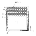
- FIGs. 2 to 5 illustrate a wired electrode of touch screen panel according to one embodiment of the present invention.
- the wired electrode of touch screen panel is formed on one surface of an substrate 100.
- the substrate 100 means a base member in the form of a plate or a film and may be formed of various materials, without limitation, e.g., a transparent material, a glass material, a plastic material, and etc.
- the wired electrode includes a contact part 10 electrically connected with a signal sensing pattern 1; a bonding part 50 for transmitting a touch signal sensed by the signal sensing pattern 1 to an external driving circuit (not shown); and a signal transmitting part 30 for connecting the contact part 10 and bonding part 50 with each other.
- the contact part 10 is a pad being in contact with one end of the signal sensing pattern 1, wherein the contact part 10 is formed of a conductive material enabling transmission of electrical signal.
- the bonding part 50 is formed on an end part of the substrate 100 to transmit the electrical signal to the external driving circuit (not shown).
- a line width of the bonding part 50 may be larger than a line width of the signal transmitting part 30.
- This structure is provided to stably connect a corresponding connection device (not shown), designed to be connected with the bonding part 50, to the bonding part 50.
- the connection device (not shown) is provided with a conductive connection line corresponding to the bonding part 50.
- the signal transmitting part 30 is a line for connecting the aforementioned contact part 10 and bonding part 50, wherein the signal transmitting part 30 is formed of a conductive material enabling transmission of the electrical signal between the contact part 10 and bonding part 50.
- the signal transmitting part 30 includes at least one curved portion 12.
- the curved portion 12 is formed by gently curving the signal transmitting part 30. A curvature degree of the signal transmitting part 30 in the curved portion 12 may be changed freely.
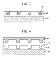
- a wired electrode including the contact part 10, signal transmitting part 30, and bonding part 50 is formed by forming a resin layer 90 on the substrate 100, forming grooves 92 on the resin layer 90, and filling the grooves 92 with a conductive material 93.
- the grooves 92 in which the wired electrode is to be formed are formed in the resin layer 90 on the substrate 100.
- an embossing mold 80 whose shape corresponds to the grooves 92 is used.
- the embossing mold with minute lines is used so as to form, on the resin layer 90, the grooves 92 in which the signal transmitting part 30 of minute lines is to be formed.
- a signal transmitting part 30 has a folded portion (See '11' of FIG. 1 ) of right angle, an embossing portion of the embossing mold 80 has been easily broken during the molding process.
- the wired electrode according to one embodiment of the present invention includes at least one curved portion 12 and has no folded portion at the signal transmitting part 30.
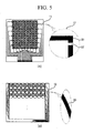
- FIG. 5 illustrates a conductive material in the groove of the wired electrode having a shape folded at right angle; and (B) illustrates a conductive material in the groove of the wired electrode having a curved portion.
- (A) of FIG. 5 the groove is filled with the conductive material to form the signal transmitting part 30.
- a non-filled portion 32 which is not filled with the conductive material, may be provided in some areas of the signal transmitting part 30.
- (A) may have a problem related with a low stability in filling of the conductive material.
- the signal transmitting part 30 is completely filled with the conductive material because a folded portion is not included in the wired electrode.
- the non-filled portion is not formed in the wired electrode according to the present invention, which enables the more stable signal transmission.
- FIG. 6 illustrates a wired electrode of touch screen panel according to another embodiment of the present invention.
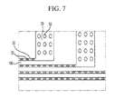
- FIG. 7 illustrates an arrangement example of wired electrode shown in FIG. 3 .
- the wired electrode of touch screen panel includes fine protrusions 32 and 52.
- the plurality of fine protrusions 32 and 52 may be formed in each of signal transmitting part 30 and bonding part 50 of the wired electrode according to another embodiment of the present invention.
- the fine protrusions 32 and 52 are formed inside a groove for formation of the aforementioned wired electrode.
- the fine protrusions 32 and 52 are formed by protrusion of partial portions of the resin layer (See '90' of FIG. 3 ) deposited on a substrate inside the groove. In this case, the fine protrusions 32 and 52 are formed by the use of aforementioned mold.
- the fine protrusions 32 and 52 are formed simultaneously with the groove which is formed in the resin layer by the embossing portion of the mold. That is, groove patterns for formation of the fine protrusions 32 and 52 are provided in the embossing portion of the mold, to thereby form the groove in the resin layer, and simultaneously form the fine protrusions 32 and 52 inside the groove.
- the groove is formed in the resin layer (See '90' of FIG. 3 ) of the substrate 100, and the groove is filled with the conductive material.
- the conductive material being in a paste state is filled in the groove, and is then cured by a curing process, whereby the cured conductive material functions as the wired electrode.
- a line width of the signal transmitting part 30 and bonding part 50 of the wired electrode is larger than a line width of grid forming the signal sensing pattern, whereby the conductive material is easily separated.
- a process for manufacturing the touch screen panel includes a cleaning step of the substrate 100, or a squeezing step using a doctor blade. During these steps, the conductive material filled in the groove of the resin layer (See FIG. 3 ) of the substrate may be separated from the groove.
- the plurality of fine protrusions 32 and 52 are formed in the signal transmitting part 30 and bonding part 50 of the wired electrode, to thereby prevent the separation of conductive material. That is, if forming the fine protrusions 32 and 52 inside the groove of the wired electrode, its line width becomes larger than the grid of signal sensing pattern so that it is possible to prevent the separation of conductive material during the process for manufacturing the touch screen panel. Accordingly, the plurality of fine protrusions 32 and 52 enable to reduce the line width of signal transmitting part 30 and bonding part 50, and simultaneously to bring the conductive material into contact with the surface of fine protrusions 32 and 52, to thereby prevent the separation of conductive material.
- a thickness of the conductive material filled in the groove will be explained with reference to FIG. 8 .
- FIG. 8 (A) is a plane view illustrating the filling state of conductive material filled in the groove and fine protrusion of the wired electrode, and (B) is a perspective view thereof.
- the conductive material may be filled in such a manner that a height of the fine protrusion 52 becomes the same as a height of the electrode formed by filling the conductive material in the groove, or a height of the electrode becomes lower than a height of the fine protrusion 52.
- the conductive material filled in the bonding part 50 is brought into close contact with the fine protrusion 52, to thereby prevent the conductive material from being separated from the bonding part 50, and to obtain good stability in filling of the wired electrode.
- FIG. 8 illustrates the fine protrusion 52 formed in the bonding part 50 of FIG. 7 . However, it can be identically applied to the fine protrusion 32 formed in the signal transmitting part 30 of FIG. 7 .
- the fine protrusions 32 and 52 may vary in shape.
- a cross-sectional shape of the fine protrusion 32 and 52 may be a circle, triangle, rectangle, semi-ellipse, semi-circle, ellipse, and etc.
- Various cross-sectional shapes of the fine protrusions 32 and 52 can increase a contact area to be in contact with the conductive material, to thereby improve a filling stability and prevent the separation of conductive material.
- the fine protrusions may be formed in shape of cylinder or cylindroid.
- the plurality of fine protrusions 32 provided in the signal transmitting part 30 may be arranged along the signal transmitting part 30.
- the shape and arrangement of the plurality of fine protrusions 52 provided in the bonding part 50 may vary.
- a horizontal cross-sectional area of the fine protrusion 52 provided in the bonding part 50 be larger than a horizontal cross-section area of the fine protrusion 32 provided in the signal transmitting part 30.
- the horizontal cross-section area indicates an area of horizontal cross section of the fine protrusion 32 and 52 when the fine protrusion 32 and 52 is cut while being parallel with the resin layer.
- a wired electrode of touch screen panel includes at least one curved portion, and a plurality of fine protrusions.
- the curved portion 12 is formed in the signal transmitting part 30 of the wired electrode, and the fine protrusions 32 and 52 are formed in each of the signal transmitting part 30 and bonding part 50.
- This embodiment of the present invention can be realized by combining the properties of the wired electrodes of touch screen panel according to the aforementioned two embodiments of the present invention. This will be easily understood by those skilled in the art, whereby a detailed explanation will not be added.
Landscapes
- Engineering & Computer Science (AREA)
- General Engineering & Computer Science (AREA)
- Theoretical Computer Science (AREA)
- Physics & Mathematics (AREA)
- Human Computer Interaction (AREA)
- General Physics & Mathematics (AREA)
- Microelectronics & Electronic Packaging (AREA)
- Manufacturing & Machinery (AREA)
- Electromagnetism (AREA)
- Computer Networks & Wireless Communication (AREA)
- Position Input By Displaying (AREA)
- Structure Of Printed Boards (AREA)
Applications Claiming Priority (2)
| Application Number | Priority Date | Filing Date | Title |
|---|---|---|---|
| KR1020110057992A KR101797651B1 (ko) | 2011-06-15 | 2011-06-15 | 터치스크린 패널용 배선 전극 및 이를 구비하는 터치스크린 패널 |
| PCT/KR2012/004719 WO2012173420A2 (fr) | 2011-06-15 | 2012-06-15 | Electrode filaire pour panneau à écran tactile |
Publications (3)
| Publication Number | Publication Date |
|---|---|
| EP2722734A2 true EP2722734A2 (fr) | 2014-04-23 |
| EP2722734A4 EP2722734A4 (fr) | 2015-03-25 |
| EP2722734B1 EP2722734B1 (fr) | 2018-01-03 |
Family
ID=47357618
Family Applications (1)
| Application Number | Title | Priority Date | Filing Date |
|---|---|---|---|
| EP12800960.2A Active EP2722734B1 (fr) | 2011-06-15 | 2012-06-15 | Electrode filaire pour panneau à écran tactile |
Country Status (7)
| Country | Link |
|---|---|
| US (1) | US9395830B2 (fr) |
| EP (1) | EP2722734B1 (fr) |
| JP (2) | JP6153518B2 (fr) |
| KR (1) | KR101797651B1 (fr) |
| CN (2) | CN103853385B (fr) |
| TW (1) | TWI559485B (fr) |
| WO (1) | WO2012173420A2 (fr) |
Cited By (3)
| Publication number | Priority date | Publication date | Assignee | Title |
|---|---|---|---|---|
| CN104391607A (zh) * | 2014-12-11 | 2015-03-04 | 山东华芯富创电子科技有限公司 | 防止银线断路触摸屏及其制作方法 |
| EP3308253A4 (fr) * | 2016-07-04 | 2019-01-16 | Boe Technology Group Co. Ltd. | Substrat tactile, panneau d'affichage tactile, appareil d'affichage tactile comportant ce substrat et ce panneau, et procédé de fabrication associé |
| CN109960438A (zh) * | 2019-03-19 | 2019-07-02 | 京东方科技集团股份有限公司 | 基板及其制作方法、触控显示装置 |
Families Citing this family (27)
| Publication number | Priority date | Publication date | Assignee | Title |
|---|---|---|---|---|
| KR101797651B1 (ko) | 2011-06-15 | 2017-11-15 | 미래나노텍(주) | 터치스크린 패널용 배선 전극 및 이를 구비하는 터치스크린 패널 |
| CN103247366B (zh) * | 2013-03-28 | 2015-04-08 | 南昌欧菲光科技有限公司 | 电容式透明导电膜及其制造方法 |
| CN103165226B (zh) * | 2013-03-28 | 2015-04-08 | 南昌欧菲光科技有限公司 | 透明导电膜及其制备方法 |
| US20140307178A1 (en) * | 2013-04-12 | 2014-10-16 | Shenzhen O-Film Tech Co., Ltd | Touch screen sensing module, manufacturing method thereof and display device |
| CN103246421B (zh) * | 2013-05-17 | 2016-10-05 | 汕头超声显示器技术有限公司 | 一种集成触控功能的偏光片及其制造方法 |
| KR101453020B1 (ko) * | 2013-06-18 | 2014-10-22 | 크루셜텍 (주) | 정전기 보호 기능을 가진 터치 검출 장치 |
| KR102187923B1 (ko) | 2013-07-16 | 2020-12-08 | 엘지이노텍 주식회사 | 터치 윈도우 |
| KR102131256B1 (ko) * | 2013-07-29 | 2020-07-07 | 엘지이노텍 주식회사 | 터치 윈도우 및 이를 포함하는 터치 디바이스 |
| CN104345939A (zh) * | 2013-07-31 | 2015-02-11 | 南昌欧菲光科技有限公司 | 一种透明导电膜及其引线电极 |
| CN104345938A (zh) * | 2013-07-31 | 2015-02-11 | 南昌欧菲光科技有限公司 | 一种透明导电膜及其引线电极 |
| WO2015030384A1 (fr) * | 2013-08-29 | 2015-03-05 | 미래나노텍 주식회사 | Électrode de câblage pour panneau à écran tactile, panneau à écran tactile l'utilisant et son procédé de fabrication |
| KR102142855B1 (ko) | 2013-08-29 | 2020-08-31 | 미래나노텍(주) | 터치스크린 패널용 배선 전극, 이를 이용한 터치스크린 패널 및 그 제조방법 |
| US9699898B2 (en) | 2013-12-27 | 2017-07-04 | Lg Chem, Ltd. | Conductive film and method for manufacturing same |
| KR102237961B1 (ko) * | 2014-01-23 | 2021-04-08 | 엘지이노텍 주식회사 | 터치 윈도우 및 이를 포함하는 디스플레이 장치 |
| US9857906B2 (en) * | 2014-01-22 | 2018-01-02 | Lg Innotek Co., Ltd. | Touch window |
| KR102302820B1 (ko) * | 2014-01-23 | 2021-09-16 | 엘지이노텍 주식회사 | 터치 윈도우 및 이를 포함하는 디스플레이 장치 |
| CN104281322B (zh) * | 2014-09-29 | 2017-10-27 | 深圳欧菲光科技股份有限公司 | 触摸屏导电结构制作方法 |
| KR101693263B1 (ko) * | 2015-02-23 | 2017-01-06 | (주)뉴옵틱스 | 도전성 시트 |
| KR20160103214A (ko) * | 2015-02-23 | 2016-09-01 | (주)뉴옵틱스 | 전도성 시트 |
| KR102313951B1 (ko) * | 2015-06-26 | 2021-10-18 | 엘지이노텍 주식회사 | 터치 윈도우 |
| JP2017076187A (ja) * | 2015-10-13 | 2017-04-20 | 大日本印刷株式会社 | 金属パターン基板の製造方法、金属パターン基板、及び、タッチ位置検出機能付き表示装置 |
| KR101817527B1 (ko) * | 2015-11-19 | 2018-01-11 | 현대자동차주식회사 | 터치 입력장치, 이를 포함하는 차량, 및 그 제조방법 |
| CN111133407B (zh) * | 2017-10-03 | 2023-08-15 | 株式会社和冠 | 用于检测笔发送出的笔信号的传感器面板 |
| CN109144323B (zh) * | 2018-09-03 | 2021-08-31 | 业成科技(成都)有限公司 | 制造电极薄膜之方法 |
| KR102621685B1 (ko) * | 2018-09-18 | 2024-01-09 | 삼성디스플레이 주식회사 | 터치스크린 및 그를 구비하는 표시장치 |
| KR102829661B1 (ko) | 2021-02-03 | 2025-07-04 | 삼성디스플레이 주식회사 | 표시 장치 |
| CN113963857B (zh) * | 2021-11-22 | 2025-07-22 | 无锡变格新材料科技有限公司 | 导电膜层的制作方法、导电膜层结构和触控传感器 |
Family Cites Families (22)
| Publication number | Priority date | Publication date | Assignee | Title |
|---|---|---|---|---|
| JPS5868057U (ja) * | 1981-11-02 | 1983-05-09 | 松下電工株式会社 | プリント配線板 |
| JP2003243785A (ja) * | 2002-02-18 | 2003-08-29 | Hitachi Cable Ltd | 樹脂接着用銅箔、銅箔/樹脂接着フィルム、および樹脂接着用銅箔の製造方法 |
| JP4449616B2 (ja) | 2004-07-21 | 2010-04-14 | パナソニック株式会社 | タッチパネル |
| US7630207B2 (en) * | 2005-09-15 | 2009-12-08 | Fujifilm Corporation | Wiring board, method of manufacturing wiring board, and liquid ejection head |
| JP2008077332A (ja) | 2006-09-20 | 2008-04-03 | Sharp Corp | タッチパネルの製造方法、タッチパネル、および、電子機器 |
| JP4682285B2 (ja) * | 2007-08-30 | 2011-05-11 | 日立電線株式会社 | 配線及び層間接続ビアの形成方法 |
| KR100936078B1 (ko) * | 2007-11-12 | 2010-01-12 | 삼성전기주식회사 | 전기부재 및 이를 이용한 인쇄회로기판의 제조방법 |
| KR20090065896A (ko) | 2007-12-18 | 2009-06-23 | 성낙훈 | 미세 회로가 형성된 필름 기판 및 그 제조방법 |
| JP5014230B2 (ja) * | 2008-04-01 | 2012-08-29 | 京セラ株式会社 | タッチパネルおよびタッチパネル型表示装置 |
| US8240036B2 (en) * | 2008-04-30 | 2012-08-14 | Panasonic Corporation | Method of producing a circuit board |
| JP5370752B2 (ja) * | 2008-06-25 | 2013-12-18 | 日立化成株式会社 | 導体層パターン付き基材、その製造法及びそれを用いた電磁波遮蔽部材 |
| TWI420373B (zh) * | 2008-07-24 | 2013-12-21 | Henghao Technology Co Ltd | 觸控面板及其製造方法 |
| JP5350138B2 (ja) * | 2008-08-26 | 2013-11-27 | パナソニック株式会社 | 電気回路の製造方法、及びその方法により得られる電気回路基板 |
| US8319747B2 (en) * | 2008-12-11 | 2012-11-27 | Apple Inc. | Single layer touch panel with segmented drive and sense electrodes |
| JP2010182137A (ja) * | 2009-02-06 | 2010-08-19 | Sony Corp | タッチパネル及びタッチパネルの製造方法 |
| US8314779B2 (en) * | 2009-02-23 | 2012-11-20 | Solomon Systech Limited | Method and apparatus for operating a touch panel |
| JP2011028474A (ja) * | 2009-07-24 | 2011-02-10 | Alps Electric Co Ltd | 入力装置及びその製造方法 |
| KR101633034B1 (ko) | 2009-10-23 | 2016-06-24 | 삼성디스플레이 주식회사 | 터치 기판, 이의 제조 방법 및 이를 갖는 표시 장치 |
| TWI416206B (zh) | 2009-11-12 | 2013-11-21 | Wintek Corp | 觸控式顯示面板 |
| TWM379119U (en) | 2009-12-11 | 2010-04-21 | Minlad Invest Ltd | Touch panel and the substrate thereof |
| US20120086649A1 (en) * | 2010-10-12 | 2012-04-12 | Innovation & Infinity Global Corp. | Conductive circuits for a touch panel and the manufacturing method thereof |
| KR101797651B1 (ko) | 2011-06-15 | 2017-11-15 | 미래나노텍(주) | 터치스크린 패널용 배선 전극 및 이를 구비하는 터치스크린 패널 |
-
2011
- 2011-06-15 KR KR1020110057992A patent/KR101797651B1/ko active Active
-
2012
- 2012-06-13 TW TW101121176A patent/TWI559485B/zh active
- 2012-06-15 JP JP2014515757A patent/JP6153518B2/ja active Active
- 2012-06-15 WO PCT/KR2012/004719 patent/WO2012173420A2/fr not_active Ceased
- 2012-06-15 EP EP12800960.2A patent/EP2722734B1/fr active Active
- 2012-06-15 CN CN201410083771.1A patent/CN103853385B/zh active Active
- 2012-06-15 US US14/125,566 patent/US9395830B2/en active Active
- 2012-06-15 CN CN201280002663.6A patent/CN103221909B/zh active Active
-
2017
- 2017-04-06 JP JP2017075744A patent/JP6359143B2/ja active Active
Cited By (3)
| Publication number | Priority date | Publication date | Assignee | Title |
|---|---|---|---|---|
| CN104391607A (zh) * | 2014-12-11 | 2015-03-04 | 山东华芯富创电子科技有限公司 | 防止银线断路触摸屏及其制作方法 |
| EP3308253A4 (fr) * | 2016-07-04 | 2019-01-16 | Boe Technology Group Co. Ltd. | Substrat tactile, panneau d'affichage tactile, appareil d'affichage tactile comportant ce substrat et ce panneau, et procédé de fabrication associé |
| CN109960438A (zh) * | 2019-03-19 | 2019-07-02 | 京东方科技集团股份有限公司 | 基板及其制作方法、触控显示装置 |
Also Published As
| Publication number | Publication date |
|---|---|
| WO2012173420A3 (fr) | 2013-04-04 |
| US20140131075A1 (en) | 2014-05-15 |
| JP6153518B2 (ja) | 2017-06-28 |
| JP6359143B2 (ja) | 2018-07-18 |
| US9395830B2 (en) | 2016-07-19 |
| KR20120138485A (ko) | 2012-12-26 |
| KR101797651B1 (ko) | 2017-11-15 |
| CN103853385B (zh) | 2015-07-15 |
| WO2012173420A2 (fr) | 2012-12-20 |
| CN103853385A (zh) | 2014-06-11 |
| TW201301473A (zh) | 2013-01-01 |
| CN103221909A (zh) | 2013-07-24 |
| JP2014519670A (ja) | 2014-08-14 |
| CN103221909B (zh) | 2016-11-02 |
| EP2722734A4 (fr) | 2015-03-25 |
| EP2722734B1 (fr) | 2018-01-03 |
| JP2017142837A (ja) | 2017-08-17 |
| TWI559485B (zh) | 2016-11-21 |
Similar Documents
| Publication | Publication Date | Title |
|---|---|---|
| US9395830B2 (en) | Wired electrode of touch screen panel | |
| CN101782819B (zh) | 触摸屏面板及其制造方法 | |
| CN105474142B (zh) | 用于触控屏幕面板的打线电极、用其的触控屏幕面板及其制造方法 | |
| KR102187680B1 (ko) | 터치 윈도우 | |
| CN103765359B (zh) | 触摸面板和用于制造该触摸面板的方法 | |
| CN105117080A (zh) | 整合压力感测功能的触控装置 | |
| CN101836178A (zh) | 包括压力传感器阵列的具有单触摸或多触摸能力的触摸屏幕或触摸垫及此类传感器的制作 | |
| TW201523374A (zh) | 指示體檢測感測器及指示體檢測裝置 | |
| KR101274945B1 (ko) | 투영 정전용량 터치 패널 및 그의 제조 방법 | |
| CN107943304A (zh) | 键盘及设置有键盘的智能移动终端 | |
| CN209570915U (zh) | 触摸面板 | |
| JP2014170334A (ja) | 静電容量式タッチパネルおよびそれを用いた手持ち式電子機器 | |
| US20120105133A1 (en) | Input device | |
| KR102212953B1 (ko) | 터치 윈도우 및 이를 포함하는 터치 디바이스 | |
| KR101295034B1 (ko) | 터치 스크린 패널용 배선전극 | |
| TWI462001B (zh) | 單片片狀投射式電容觸控面板結構及其製作方法 | |
| KR102111402B1 (ko) | 터치 스크린 패널용 배선전극 | |
| KR20180113081A (ko) | 터치 패널 | |
| KR20170096476A (ko) | 터치 압력 감지 센서 및 이를 포함하는 터치 스크린 패널 | |
| KR101223315B1 (ko) | 입력 장치 | |
| KR102187470B1 (ko) | 터치 윈도우 | |
| US9360974B2 (en) | Touch panel and method of manufacturing the same | |
| CN110413157A (zh) | 一种带有凹凸触控键的电容触摸屏 | |
| CN102339186A (zh) | 一种单层ito的布线结构 | |
| KR20160090174A (ko) | 터치 윈도우 |
Legal Events
| Date | Code | Title | Description |
|---|---|---|---|
| PUAI | Public reference made under article 153(3) epc to a published international application that has entered the european phase |
Free format text: ORIGINAL CODE: 0009012 |
|
| 17P | Request for examination filed |
Effective date: 20131230 |
|
| AK | Designated contracting states |
Kind code of ref document: A2 Designated state(s): AL AT BE BG CH CY CZ DE DK EE ES FI FR GB GR HR HU IE IS IT LI LT LU LV MC MK MT NL NO PL PT RO RS SE SI SK SM TR |
|
| DAX | Request for extension of the european patent (deleted) | ||
| REG | Reference to a national code |
Ref country code: DE Ref legal event code: R079 Ref document number: 602012041650 Country of ref document: DE Free format text: PREVIOUS MAIN CLASS: G06F0003041000 Ipc: G06F0003044000 |
|
| A4 | Supplementary search report drawn up and despatched |
Effective date: 20150224 |
|
| RIC1 | Information provided on ipc code assigned before grant |
Ipc: H05K 3/12 20060101ALI20150218BHEP Ipc: G06F 3/044 20060101AFI20150218BHEP Ipc: H05K 1/02 20060101ALI20150218BHEP |
|
| 17Q | First examination report despatched |
Effective date: 20160823 |
|
| GRAP | Despatch of communication of intention to grant a patent |
Free format text: ORIGINAL CODE: EPIDOSNIGR1 |
|
| INTG | Intention to grant announced |
Effective date: 20170711 |
|
| GRAS | Grant fee paid |
Free format text: ORIGINAL CODE: EPIDOSNIGR3 |
|
| GRAA | (expected) grant |
Free format text: ORIGINAL CODE: 0009210 |
|
| AK | Designated contracting states |
Kind code of ref document: B1 Designated state(s): AL AT BE BG CH CY CZ DE DK EE ES FI FR GB GR HR HU IE IS IT LI LT LU LV MC MK MT NL NO PL PT RO RS SE SI SK SM TR |
|
| REG | Reference to a national code |
Ref country code: GB Ref legal event code: FG4D |
|
| REG | Reference to a national code |
Ref country code: CH Ref legal event code: EP Ref country code: AT Ref legal event code: REF Ref document number: 960875 Country of ref document: AT Kind code of ref document: T Effective date: 20180115 |
|
| REG | Reference to a national code |
Ref country code: IE Ref legal event code: FG4D |
|
| REG | Reference to a national code |
Ref country code: DE Ref legal event code: R096 Ref document number: 602012041650 Country of ref document: DE |
|
| REG | Reference to a national code |
Ref country code: NL Ref legal event code: MP Effective date: 20180103 |
|
| REG | Reference to a national code |
Ref country code: LT Ref legal event code: MG4D |
|
| REG | Reference to a national code |
Ref country code: AT Ref legal event code: MK05 Ref document number: 960875 Country of ref document: AT Kind code of ref document: T Effective date: 20180103 |
|
| REG | Reference to a national code |
Ref country code: FR Ref legal event code: PLFP Year of fee payment: 7 |
|
| PG25 | Lapsed in a contracting state [announced via postgrant information from national office to epo] |
Ref country code: NL Free format text: LAPSE BECAUSE OF FAILURE TO SUBMIT A TRANSLATION OF THE DESCRIPTION OR TO PAY THE FEE WITHIN THE PRESCRIBED TIME-LIMIT Effective date: 20180103 |
|
| PG25 | Lapsed in a contracting state [announced via postgrant information from national office to epo] |
Ref country code: FI Free format text: LAPSE BECAUSE OF FAILURE TO SUBMIT A TRANSLATION OF THE DESCRIPTION OR TO PAY THE FEE WITHIN THE PRESCRIBED TIME-LIMIT Effective date: 20180103 Ref country code: LT Free format text: LAPSE BECAUSE OF FAILURE TO SUBMIT A TRANSLATION OF THE DESCRIPTION OR TO PAY THE FEE WITHIN THE PRESCRIBED TIME-LIMIT Effective date: 20180103 Ref country code: HR Free format text: LAPSE BECAUSE OF FAILURE TO SUBMIT A TRANSLATION OF THE DESCRIPTION OR TO PAY THE FEE WITHIN THE PRESCRIBED TIME-LIMIT Effective date: 20180103 Ref country code: CY Free format text: LAPSE BECAUSE OF FAILURE TO SUBMIT A TRANSLATION OF THE DESCRIPTION OR TO PAY THE FEE WITHIN THE PRESCRIBED TIME-LIMIT Effective date: 20180103 Ref country code: NO Free format text: LAPSE BECAUSE OF FAILURE TO SUBMIT A TRANSLATION OF THE DESCRIPTION OR TO PAY THE FEE WITHIN THE PRESCRIBED TIME-LIMIT Effective date: 20180403 Ref country code: ES Free format text: LAPSE BECAUSE OF FAILURE TO SUBMIT A TRANSLATION OF THE DESCRIPTION OR TO PAY THE FEE WITHIN THE PRESCRIBED TIME-LIMIT Effective date: 20180103 |
|
| PG25 | Lapsed in a contracting state [announced via postgrant information from national office to epo] |
Ref country code: IS Free format text: LAPSE BECAUSE OF FAILURE TO SUBMIT A TRANSLATION OF THE DESCRIPTION OR TO PAY THE FEE WITHIN THE PRESCRIBED TIME-LIMIT Effective date: 20180503 Ref country code: BG Free format text: LAPSE BECAUSE OF FAILURE TO SUBMIT A TRANSLATION OF THE DESCRIPTION OR TO PAY THE FEE WITHIN THE PRESCRIBED TIME-LIMIT Effective date: 20180403 Ref country code: AT Free format text: LAPSE BECAUSE OF FAILURE TO SUBMIT A TRANSLATION OF THE DESCRIPTION OR TO PAY THE FEE WITHIN THE PRESCRIBED TIME-LIMIT Effective date: 20180103 Ref country code: RS Free format text: LAPSE BECAUSE OF FAILURE TO SUBMIT A TRANSLATION OF THE DESCRIPTION OR TO PAY THE FEE WITHIN THE PRESCRIBED TIME-LIMIT Effective date: 20180103 Ref country code: SE Free format text: LAPSE BECAUSE OF FAILURE TO SUBMIT A TRANSLATION OF THE DESCRIPTION OR TO PAY THE FEE WITHIN THE PRESCRIBED TIME-LIMIT Effective date: 20180103 Ref country code: LV Free format text: LAPSE BECAUSE OF FAILURE TO SUBMIT A TRANSLATION OF THE DESCRIPTION OR TO PAY THE FEE WITHIN THE PRESCRIBED TIME-LIMIT Effective date: 20180103 Ref country code: GR Free format text: LAPSE BECAUSE OF FAILURE TO SUBMIT A TRANSLATION OF THE DESCRIPTION OR TO PAY THE FEE WITHIN THE PRESCRIBED TIME-LIMIT Effective date: 20180404 Ref country code: PL Free format text: LAPSE BECAUSE OF FAILURE TO SUBMIT A TRANSLATION OF THE DESCRIPTION OR TO PAY THE FEE WITHIN THE PRESCRIBED TIME-LIMIT Effective date: 20180103 |
|
| REG | Reference to a national code |
Ref country code: DE Ref legal event code: R097 Ref document number: 602012041650 Country of ref document: DE |
|
| PG25 | Lapsed in a contracting state [announced via postgrant information from national office to epo] |
Ref country code: EE Free format text: LAPSE BECAUSE OF FAILURE TO SUBMIT A TRANSLATION OF THE DESCRIPTION OR TO PAY THE FEE WITHIN THE PRESCRIBED TIME-LIMIT Effective date: 20180103 Ref country code: RO Free format text: LAPSE BECAUSE OF FAILURE TO SUBMIT A TRANSLATION OF THE DESCRIPTION OR TO PAY THE FEE WITHIN THE PRESCRIBED TIME-LIMIT Effective date: 20180103 Ref country code: AL Free format text: LAPSE BECAUSE OF FAILURE TO SUBMIT A TRANSLATION OF THE DESCRIPTION OR TO PAY THE FEE WITHIN THE PRESCRIBED TIME-LIMIT Effective date: 20180103 |
|
| PLBE | No opposition filed within time limit |
Free format text: ORIGINAL CODE: 0009261 |
|
| STAA | Information on the status of an ep patent application or granted ep patent |
Free format text: STATUS: NO OPPOSITION FILED WITHIN TIME LIMIT |
|
| PG25 | Lapsed in a contracting state [announced via postgrant information from national office to epo] |
Ref country code: DK Free format text: LAPSE BECAUSE OF FAILURE TO SUBMIT A TRANSLATION OF THE DESCRIPTION OR TO PAY THE FEE WITHIN THE PRESCRIBED TIME-LIMIT Effective date: 20180103 Ref country code: SK Free format text: LAPSE BECAUSE OF FAILURE TO SUBMIT A TRANSLATION OF THE DESCRIPTION OR TO PAY THE FEE WITHIN THE PRESCRIBED TIME-LIMIT Effective date: 20180103 Ref country code: SM Free format text: LAPSE BECAUSE OF FAILURE TO SUBMIT A TRANSLATION OF THE DESCRIPTION OR TO PAY THE FEE WITHIN THE PRESCRIBED TIME-LIMIT Effective date: 20180103 Ref country code: CZ Free format text: LAPSE BECAUSE OF FAILURE TO SUBMIT A TRANSLATION OF THE DESCRIPTION OR TO PAY THE FEE WITHIN THE PRESCRIBED TIME-LIMIT Effective date: 20180103 |
|
| 26N | No opposition filed |
Effective date: 20181005 |
|
| REG | Reference to a national code |
Ref country code: CH Ref legal event code: PL |
|
| PG25 | Lapsed in a contracting state [announced via postgrant information from national office to epo] |
Ref country code: SI Free format text: LAPSE BECAUSE OF FAILURE TO SUBMIT A TRANSLATION OF THE DESCRIPTION OR TO PAY THE FEE WITHIN THE PRESCRIBED TIME-LIMIT Effective date: 20180103 |
|
| REG | Reference to a national code |
Ref country code: BE Ref legal event code: MM Effective date: 20180630 |
|
| REG | Reference to a national code |
Ref country code: IE Ref legal event code: MM4A |
|
| PG25 | Lapsed in a contracting state [announced via postgrant information from national office to epo] |
Ref country code: MC Free format text: LAPSE BECAUSE OF FAILURE TO SUBMIT A TRANSLATION OF THE DESCRIPTION OR TO PAY THE FEE WITHIN THE PRESCRIBED TIME-LIMIT Effective date: 20180103 Ref country code: LU Free format text: LAPSE BECAUSE OF NON-PAYMENT OF DUE FEES Effective date: 20180615 |
|
| PG25 | Lapsed in a contracting state [announced via postgrant information from national office to epo] |
Ref country code: IE Free format text: LAPSE BECAUSE OF NON-PAYMENT OF DUE FEES Effective date: 20180615 Ref country code: CH Free format text: LAPSE BECAUSE OF NON-PAYMENT OF DUE FEES Effective date: 20180630 Ref country code: LI Free format text: LAPSE BECAUSE OF NON-PAYMENT OF DUE FEES Effective date: 20180630 |
|
| PG25 | Lapsed in a contracting state [announced via postgrant information from national office to epo] |
Ref country code: BE Free format text: LAPSE BECAUSE OF NON-PAYMENT OF DUE FEES Effective date: 20180630 |
|
| PG25 | Lapsed in a contracting state [announced via postgrant information from national office to epo] |
Ref country code: MT Free format text: LAPSE BECAUSE OF NON-PAYMENT OF DUE FEES Effective date: 20180615 |
|
| PG25 | Lapsed in a contracting state [announced via postgrant information from national office to epo] |
Ref country code: TR Free format text: LAPSE BECAUSE OF FAILURE TO SUBMIT A TRANSLATION OF THE DESCRIPTION OR TO PAY THE FEE WITHIN THE PRESCRIBED TIME-LIMIT Effective date: 20180103 |
|
| PG25 | Lapsed in a contracting state [announced via postgrant information from national office to epo] |
Ref country code: PT Free format text: LAPSE BECAUSE OF FAILURE TO SUBMIT A TRANSLATION OF THE DESCRIPTION OR TO PAY THE FEE WITHIN THE PRESCRIBED TIME-LIMIT Effective date: 20180103 Ref country code: HU Free format text: LAPSE BECAUSE OF FAILURE TO SUBMIT A TRANSLATION OF THE DESCRIPTION OR TO PAY THE FEE WITHIN THE PRESCRIBED TIME-LIMIT; INVALID AB INITIO Effective date: 20120615 |
|
| PG25 | Lapsed in a contracting state [announced via postgrant information from national office to epo] |
Ref country code: MK Free format text: LAPSE BECAUSE OF NON-PAYMENT OF DUE FEES Effective date: 20180103 |
|
| PGFP | Annual fee paid to national office [announced via postgrant information from national office to epo] |
Ref country code: GB Payment date: 20240620 Year of fee payment: 13 |
|
| PGFP | Annual fee paid to national office [announced via postgrant information from national office to epo] |
Ref country code: FR Payment date: 20240621 Year of fee payment: 13 |
|
| PGFP | Annual fee paid to national office [announced via postgrant information from national office to epo] |
Ref country code: IT Payment date: 20240628 Year of fee payment: 13 |
|
| PGFP | Annual fee paid to national office [announced via postgrant information from national office to epo] |
Ref country code: DE Payment date: 20250618 Year of fee payment: 14 |
|
| GBPC | Gb: european patent ceased through non-payment of renewal fee |
Effective date: 20250615 |
|
| PG25 | Lapsed in a contracting state [announced via postgrant information from national office to epo] |
Ref country code: GB Free format text: LAPSE BECAUSE OF NON-PAYMENT OF DUE FEES Effective date: 20250615 |
|
| PG25 | Lapsed in a contracting state [announced via postgrant information from national office to epo] |
Ref country code: IT Free format text: LAPSE BECAUSE OF NON-PAYMENT OF DUE FEES Effective date: 20250615 |
|
| PG25 | Lapsed in a contracting state [announced via postgrant information from national office to epo] |
Ref country code: FR Free format text: LAPSE BECAUSE OF NON-PAYMENT OF DUE FEES Effective date: 20250630 |