EP2722907A2 - Organische lichtemittierende Diodenanzeige und Herstellungsverfahren dafür - Google Patents
Organische lichtemittierende Diodenanzeige und Herstellungsverfahren dafür Download PDFInfo
- Publication number
- EP2722907A2 EP2722907A2 EP13188811.7A EP13188811A EP2722907A2 EP 2722907 A2 EP2722907 A2 EP 2722907A2 EP 13188811 A EP13188811 A EP 13188811A EP 2722907 A2 EP2722907 A2 EP 2722907A2
- Authority
- EP
- European Patent Office
- Prior art keywords
- porous region
- substrate
- equal
- pores
- layer
- Prior art date
- Legal status (The legal status is an assumption and is not a legal conclusion. Google has not performed a legal analysis and makes no representation as to the accuracy of the status listed.)
- Withdrawn
Links
- 238000004519 manufacturing process Methods 0.000 title claims abstract description 21
- 239000000758 substrate Substances 0.000 claims abstract description 93
- 239000011148 porous material Substances 0.000 claims abstract description 62
- 239000000463 material Substances 0.000 claims description 30
- 239000002184 metal Substances 0.000 claims description 20
- 238000005538 encapsulation Methods 0.000 claims description 9
- 238000010438 heat treatment Methods 0.000 claims description 7
- XUIMIQQOPSSXEZ-UHFFFAOYSA-N Silicon Chemical compound [Si] XUIMIQQOPSSXEZ-UHFFFAOYSA-N 0.000 claims description 5
- 229910052710 silicon Inorganic materials 0.000 claims description 5
- 239000010703 silicon Substances 0.000 claims description 5
- 239000011521 glass Substances 0.000 claims description 4
- 238000000034 method Methods 0.000 description 8
- 230000003578 releasing effect Effects 0.000 description 7
- 150000004767 nitrides Chemical class 0.000 description 5
- 238000000149 argon plasma sintering Methods 0.000 description 2
- 238000005336 cracking Methods 0.000 description 2
- 238000010586 diagram Methods 0.000 description 2
- 238000012986 modification Methods 0.000 description 2
- 230000004048 modification Effects 0.000 description 2
- 230000003247 decreasing effect Effects 0.000 description 1
- 238000002372 labelling Methods 0.000 description 1
- 238000002844 melting Methods 0.000 description 1
- 230000008018 melting Effects 0.000 description 1
Images



Classifications
-
- H—ELECTRICITY
- H10—SEMICONDUCTOR DEVICES; ELECTRIC SOLID-STATE DEVICES NOT OTHERWISE PROVIDED FOR
- H10K—ORGANIC ELECTRIC SOLID-STATE DEVICES
- H10K59/00—Integrated devices, or assemblies of multiple devices, comprising at least one organic light-emitting element covered by group H10K50/00
- H10K59/80—Constructional details
- H10K59/87—Passivation; Containers; Encapsulations
- H10K59/871—Self-supporting sealing arrangements
- H10K59/8722—Peripheral sealing arrangements, e.g. adhesives, sealants
-
- H—ELECTRICITY
- H10—SEMICONDUCTOR DEVICES; ELECTRIC SOLID-STATE DEVICES NOT OTHERWISE PROVIDED FOR
- H10K—ORGANIC ELECTRIC SOLID-STATE DEVICES
- H10K50/00—Organic light-emitting devices
- H10K50/80—Constructional details
- H10K50/84—Passivation; Containers; Encapsulations
- H10K50/842—Containers
- H10K50/8426—Peripheral sealing arrangements, e.g. adhesives, sealants
-
- H—ELECTRICITY
- H10—SEMICONDUCTOR DEVICES; ELECTRIC SOLID-STATE DEVICES NOT OTHERWISE PROVIDED FOR
- H10K—ORGANIC ELECTRIC SOLID-STATE DEVICES
- H10K50/00—Organic light-emitting devices
- H10K50/80—Constructional details
- H10K50/84—Passivation; Containers; Encapsulations
- H10K50/844—Encapsulations
-
- H—ELECTRICITY
- H10—SEMICONDUCTOR DEVICES; ELECTRIC SOLID-STATE DEVICES NOT OTHERWISE PROVIDED FOR
- H10K—ORGANIC ELECTRIC SOLID-STATE DEVICES
- H10K59/00—Integrated devices, or assemblies of multiple devices, comprising at least one organic light-emitting element covered by group H10K50/00
-
- H—ELECTRICITY
- H10—SEMICONDUCTOR DEVICES; ELECTRIC SOLID-STATE DEVICES NOT OTHERWISE PROVIDED FOR
- H10K—ORGANIC ELECTRIC SOLID-STATE DEVICES
- H10K59/00—Integrated devices, or assemblies of multiple devices, comprising at least one organic light-emitting element covered by group H10K50/00
- H10K59/10—OLED displays
- H10K59/12—Active-matrix OLED [AMOLED] displays
- H10K59/131—Interconnections, e.g. wiring lines or terminals
-
- H—ELECTRICITY
- H10—SEMICONDUCTOR DEVICES; ELECTRIC SOLID-STATE DEVICES NOT OTHERWISE PROVIDED FOR
- H10K—ORGANIC ELECTRIC SOLID-STATE DEVICES
- H10K59/00—Integrated devices, or assemblies of multiple devices, comprising at least one organic light-emitting element covered by group H10K50/00
- H10K59/10—OLED displays
- H10K59/17—Passive-matrix OLED displays
- H10K59/179—Interconnections, e.g. wiring lines or terminals
-
- H—ELECTRICITY
- H10—SEMICONDUCTOR DEVICES; ELECTRIC SOLID-STATE DEVICES NOT OTHERWISE PROVIDED FOR
- H10K—ORGANIC ELECTRIC SOLID-STATE DEVICES
- H10K71/00—Manufacture or treatment specially adapted for the organic devices covered by this subclass
-
- H—ELECTRICITY
- H10—SEMICONDUCTOR DEVICES; ELECTRIC SOLID-STATE DEVICES NOT OTHERWISE PROVIDED FOR
- H10K—ORGANIC ELECTRIC SOLID-STATE DEVICES
- H10K59/00—Integrated devices, or assemblies of multiple devices, comprising at least one organic light-emitting element covered by group H10K50/00
- H10K59/80—Constructional details
- H10K59/87—Passivation; Containers; Encapsulations
- H10K59/873—Encapsulations
-
- H—ELECTRICITY
- H10—SEMICONDUCTOR DEVICES; ELECTRIC SOLID-STATE DEVICES NOT OTHERWISE PROVIDED FOR
- H10K—ORGANIC ELECTRIC SOLID-STATE DEVICES
- H10K71/00—Manufacture or treatment specially adapted for the organic devices covered by this subclass
- H10K71/40—Thermal treatment, e.g. annealing in the presence of a solvent vapour
- H10K71/421—Thermal treatment, e.g. annealing in the presence of a solvent vapour using coherent electromagnetic radiation, e.g. laser annealing
Definitions
- the invention relates in general to an organic light emitting diode display and a manufacturing method thereof, and particularly to an organic light emitting diode display comprising a frit layer having a porous structure and a manufacturing method thereof.
- Organic light emitting diode displays have become one of the most important research targets of display technology, and the requirements to the functions and characteristics of organic light emitting diode displays have gradually increased as well.
- organic light emitting diodes are very sensitive to moisture, and hence the performance and the service life thereof are easily influenced by external moisture. Therefore, researchers have been working on providing an organic light emitting diode display with excellent moisture-resisting abilities.
- the invention relates to an organic light emitting diode display and a manufacturing method thereof.
- the organic light emitting diode display with the "loose-dense-loose" structure formed from the first and the third porous regions having large pores and the second porous region having small pores and located between the first and the third porous regions, both moisture resistance and strain releasing can be achieved at the same time.
- an organic light emitting diode display comprises a first substrate, a second substrate, and a frit layer.
- the first substrate has a displaying area.
- the frit layer adheres the first substrate and the second substrate to each other.
- the frit layer comprises a first porous region and a second porous region disposed adjacent to the first porous region.
- the first porous region is disposed on the displaying area and located between the second porous region and the displaying area.
- the first porous region has a plurality of first pores with a diameter of larger than or equal to 4 ⁇ m and smaller than or equal to 15 ⁇ m.
- the number of the first pores with the diameter of larger than or equal to 4 ⁇ m and smaller than or equal to 15 ⁇ m is greater than the number of the pores of the second porous region with the diameter of larger than or equal to 4 ⁇ m and smaller than or equal to 15 ⁇ m.
- a manufacturing method of an organic light emitting diode display comprises the following steps: a first substrate having a displaying area and a second substrate are provided; a plurality of organic light emitting diodes are disposed on the first substrate; and a frit layer is formed for adhering the first substrate and the second substrate to each other.
- Forming the frit layer includes the following steps: a first porous region having a plurality of first pores with a diameter of larger than or equal to 4 ⁇ m and smaller than or equal to 15 ⁇ m is formed; and a second porous region is formed adjacent to the first porous region.
- the number of the first pores with the diameter of larger than or equal to 4 ⁇ m and smaller than or equal to 15 ⁇ m is greater than the number of the pores of the second porous region with the diameter of larger than or equal to 4 ⁇ m and smaller than or equal to 15 ⁇ m.
- FIG. 1A shows a top view of an organic light emitting diode display according to an embodiment of the present invention
- FIG. 1B shows a cross-sectional view along the section line 1B-1B' in FIG. 1A ;
- FIG. 2A shows a top view of an organic light emitting diode display according to another embodiment of the present invention
- FIG. 2B shows a cross-sectional view along the section line 2B-2B' in FIG. 2A ;
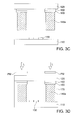
- FIGS. 3A-3E illustrate a process for manufacturing an organic light emitting diode display according to an embodiment of the present invention.
- FIG. 4 shows a partial schematic diagram of a laser beam passing through a patterned mask for forming a frit layer according to an embodiment of the present invention.
- an organic light emitting diode display and a manufacturing method thereof are provided.
- the organic light emitting diode display with the "loose-dense-loose" structure formed from the first and the third porous regions having large pores and the second porous region having small pores and located between the first and the third porous regions, both moisture resistance and strain releasing can be achieved at the same time.
- the following embodiments are for the purpose of elaboration only, not for limiting the scope of protection of the invention. Detailed structures and processes may be modified or changed by one skilled in the art after having the benefit of this description of the disclosure.
- FIG. 1A shows a top view of an organic light emitting diode display according to an embodiment of the present invention
- FIG. 1B shows a cross-sectional view along the section line 1B-1B' in FIG. 1A
- the organic light emitting diode display 100 includes a first substrate 110, a second substrate 120, one or more than one organic light emitting diode 130, and a frit layer 140.
- the first substrate 110 has a displaying area D.
- the organic light emitting diode 130 is disposed on the first substrate 110.
- the frit layer 140 adheres the first substrate 110 and the second substrate 120 to each other.
- the frit layer 140 includes a first porous region 141, a second porous region 143, and a third porous region 145.
- the first porous region 141 is disposed adjacent to the displaying area D, and the first porous region 141 is disposed between the second porous region 143 and the displaying area D.
- the first porous region 141 has a plurality of first pores 141a with a diameter of larger than or equal to 4 ⁇ m and smaller than or equal to 15 ⁇ m.
- the second porous region 143 has a plurality of second pores 143a with a diameter of larger than or equal to 0.2 ⁇ m and smaller than or equal to 4 ⁇ m.
- the third porous region 145 is located on an outermost side of the frit layer 140, and the second porous region 143 is located between the first porous region 141 and the third porous region 145.
- the third porous region 145 has a plurality of third pores 145a with the diameter of larger than or equal to 4 ⁇ m and smaller than or equal to 15 ⁇ m.
- the frit layer 140 is formed between the first substrate 110 and the second substrate 120 and surrounding the organic light emitting diodes 130.
- the material of the frit layer 140 comprises, for example, a silicon-containing material with excellent moisture resistance properties.
- the first substrate 110 and the second substrate 120 are such as glass substrates. Similar to the frit layer 140, the first substrate 110 and the second substrate 120 comprise a silicon-containing material. Such homogeneity of materials provides excellent moisture resistance properties of the whole structure after the substrates 110, 120 and the frit layer 140 are adhered to each other.
- the material selections of the first substrate 110, the second substrate 120, and the frit layer 140 are depending on the conditions applied and are not limited to the materials aforementioned.
- the material of the frit layer 140 includes a silicon-containing material, which provides excellent moisture resistance. However, after the frit layer 140 is heated to be adhered to glass substrates (e.g. the first substrate 110 and the second substrate 120), it may deform or even crack under the strain. Once the frit layer 140 is deformed or cracked, the moisture resistance of the whole structure is largely reduced.
- the first porous region 141 and the third porous region 145 are located on the two sides of the second porous region 143, and the number of the pores 141a and 145a, which have diameters of larger than or equal to 4 ⁇ m and smaller than or equal to 15 ⁇ m, of the first porous region 141 and the third porous region 145 is greater than the number of the pores with the above-mentioned diameter range (4-15 ⁇ m) of the second porous region 143.
- the number of the pores, which have diameters of larger than or equal to 0.2 ⁇ m and smaller than or equal to 4 ⁇ m, of the second porous region 143 is larger than the pores with the above-mentioned diameter range (0.2-4 ⁇ m) of the first porous region 141 and the third porous region 145.
- the pores with large diameters of the first porous region 141 and the third porous region 145 may release the strain effectively, reducing the deformation and cracking of the whole structure under strain.
- the first porous region 141 and the third porous region 145, having large pores, located on two sides may be regarded as loose springs
- the second porous region 143, having small pores, located in the middle may be regarded as a tight spring. Accordingly, the frit layer 140 as a whole has a "loose-dense-loose" structure and is provided with a better strain releasing effect, compared to a conventional spring structure with single tension condition.
- the porous structure of the frit layer 140 can release the strain effectively and reduce the deformation and cracking when the whole structure is under strain. However, too many pores make the whole structure less dense to an unacceptable level, resulting in decreasing the strain releasing effect, while too few pores make the strain releasing effect decrease.
- the number of the pores with diameters of larger than or equal to 4 ⁇ m and smaller than or equal to 15 ⁇ m of the first porous region 141 and the third porous region 145 is greater than the number of the pores with the above-mentioned diameter range (4-15 ⁇ m) of the second porous region 143, and the number of the pores with diameters of larger than or equal to 0.2 ⁇ m and smaller than or equal to 4 ⁇ m of the second porous region 143 is greater than the pores with the above-mentioned diameter range (0.2-4 ⁇ m) of the first porous region 141 and the third porous region 145.
- the small pores of the second porous region 143 provide a dense structure of the second porous region 143, and thus excellent moisture resistance is maintained.
- the "loose-dense-loose" structure formed from the first porous region 141, the second porous region 143, and the third porous region 145 can achieve excellent moisture resistance t while the strain is effectively released at the same time.
- the first porous region 141 has a width W1
- the second porous region 143 has a width W2
- the third porous region 145 has a width W3.
- a ratio of the width W2 of the second porous region 143 to the width (W1+W2+E3) of the frit layer 140 is, for example, 10-90%.
- the ratio of the width W2 of the second porous region 143 to the width (W1+W2+E3) of the frit layer 140 is, for example, 25-35%, resulting in a better strain releasing effect.
- the third porous region 145 surrounds the second porous region 143
- the second porous region 143 surrounds the first porous region 141
- the first porous region 141 surrounds the organic light emitting diodes 130.
- the frit layer 140 surrounding the organic light emitting diodes 130 has, for example, a square hollow structure, and the corner portion of such square hollow structure has a greater density of pores. Since the corner portion is usually under a larger strain, with a greater density of pores, the strain releasing ability of the corner portion is hence improved.
- the first porous region 141, the second porous region 143, and the third porous region 143 abut against the first substrate 110 and the second substrate 120.
- FIG. 2A shows a top view of an organic light emitting diode display according to another embodiment of the present invention
- FIG. 2B shows a cross-sectional view along the section line 2B-2B' in FIG. 2A
- the organic light emitting diode display 100' includes the first substrate 110, the second substrate 120, one or more than one organic light emitting diode 130, and the frit layer 140.
- the structures, arrangements, and function theories of the above-mentioned elements are similar to those with the same labeling in FIGS. 1A-1B and are not repeated there. The differences of the present embodiment from the previous embodiment are described below.
- the organic light emitting diode display 100' may include a metal layer 150 and a fan out wire structure 180.
- the fan out wire structure 180 and the metal layer are disposed between the frit layer 140 and the second substrate 120.
- the fan out wire structure 180 is electrically connected to the organic light emitting diodes 130.
- the metal layer 150 is electrically isolated from other electronic components.
- the fan out wire structure 180 is located below a portion of the frit layer 140, while the metal layer 150 is located below the left portion of the frit layer 140.
- the fan out wire structure 180 below the frit layer 140 reflects the laser beam, such that the heating efficiency of the portion of the frit layer 140 located above the fan out wire structure 180 is higher than the left portion of the frit layer 140.
- the metal layer 150 is disposed below the left portion of the frit layer 140 where the fan out wire structure is not disposed. As such, the whole area below the whole frit layer 140 is disposed with metal (including the fan out wire structure 180 and the metal layer 150), such that the heating efficiency of the whole frit layer 140 in the heating process by the laser beam is uniform.
- the organic light emitting diode display 100' may include a metal nitride layer 160 disposed between the frit layer 140 and the metal layer 150.
- the metal nitride layer 160 can increase the adhesion between the frit layer 140 and the metal layer 150.
- the organic light emitting diode display 100' may further include an encapsulation layer 170 disposed between the first substrate 110 and the second substrate 120.
- the encapsulation layer 170 surrounds and covers the frit layer 140.
- the encapsulation layer 170 can increase the moisture resistance of the whole device.
- FIGS. 3A-3E illustrate a process for manufacturing an organic light emitting diode display according to an embodiment of the invention.
- the first substrate 110 and the second substrate 120 are provided, and one or more than one organic light emitting diode 130 is disposed on the first substrate 110.
- the metal layer 150 may be formed on the second substrate 120, optionally.
- the metal layer 150 is formed, for example, between the frit layer, which will be formed in the following process, and the second substrate 120.
- the metal nitride layer 160 may be formed on the metal layer 150, optionally.
- the metal nitride layer 160 is formed, for example, between the frit layer 140, which will be formed in the following process, and the metal layer 150.
- the frit layer 140 is formed for adhering the first substrate 110 and the second substrate 120 to each other.
- the manufacturing method of forming the frit layer 140 includes, for example: forming the first porous region 141, forming the second porous region 143 adjacent to the first porous region 141, and forming the third porous region 145 adjacent to the second porous region 143, the second porous region 143 being located between the first porous region 141 and the third porous region 145.
- the first porous region 141 has the first pores 141a with diameters of larger than or equal to 4 ⁇ m and smaller than or equal to 15 ⁇ m.
- the second porous region 143 has the second pores 143a with diameters of larger than or equal to 0.2 ⁇ m and smaller than or equal to 4 ⁇ m.
- the third porous region 145 has the third pores 145a with diameters of larger than or equal to 4 ⁇ m and smaller than or equal to 15 ⁇ m.
- the steps of forming the first porous region 141, forming the second porous region 143, and forming the third porous region 145 are carried out simultaneously.
- the frit layer 140 is formed, for example, between the first substrate 110 and the second substrate 120 and surrounds the organic light emitting diodes 130.
- the manufacturing method of forming the frit layer 140 includes such as the following steps. As shown in FIG. 3C , a frit material layer 140a is formed on the second substrate 120. In an embodiment, the frit material layer 140a is formed on the metal layer 150 and the metal nitride layer 160. Next, the frit material layer 140a is preheated. In the embodiment, the frit material layer 140a is preheated at a temperature of, for example, 460-500°C. The frit material layer 140a is preheated to be coagulated on the surface of the second substrate 120, such that the frit material layer 140a will not overflow when the second substrate 120 is flipped over in the following assembling process.
- the frit material layer 140a is heated to form the frit layer 140 adhering the first substrate 110 and the second substrate 120 to each other.
- the frit material layer 140a is heated by, such as, the laser beam L to form the frit layer 140.
- the frit material layer 140a is heated by the laser beam L at a temperature higher than the preheating temperature.
- the frit material layer 140a comprises a silicon-containing material, and the first substrate 110 and the second substrate 120 are glass substrates.
- the homogeneity of the materials of the frit material layer 140a, the first substrate 110, and the second substrate 120 causes the three layers turn into a melting state as heated, and therefore, the frit material layer 140a perfectly adheres the first substrate 110 and the second substrate 120 to each other, and the whole structure after adhering has excellent moisture resistance.
- the energy of the laser beam L is higher when the laser beam L is irradiated on the first porous region 141 and on the third porous region 145, and the energy of the laser beam L is lower when the laser beam L is irradiated on the second porous region 143, such that the average pore size of the pores of the first porous region 141 and the third porous region 145 is larger, and the average pore size of the pores of the second porous region 143 is smaller.
- the laser beam L may include a plurality of laser pulses continuously irradiated on the frit material layer 140a.
- the frit material layer 140a may be heated by the laser beam L passing through a patterned mask PM to form the first porous region 141, the second porous region 143, and the third porous region 145, as shown in FIG. 3D .
- the patterned mask PM may have a plurality of slits (referring to FIG. 4 ), and the laser beam L passes the slits to heat the frit material layer 140a.
- FIG. 4 shows a partial schematic diagram of a laser beam passing through a patterned mask for forming a frit layer according to an embodiment of the present invention.
- each patterned mask PM has, for example, two slits S, and the locations of the two slits S are corresponding to the predetermined positions of the first porous region 141 and the second porous region 143, respectively.
- the laser beam L passes through the two slits S and is divided into a plurality of laser beams heating different regions of the frit material layer 140a, respectively, to form the frit layer 140.
- the laser beam L1 irradiates on the first porous region 141 and the third porous region 145.
- the pores of the first porous region 141 and the third porous region 145 have a larger size.
- the laser beam L2 irradiates on the second porous region 143. Since the travelling path of the laser beam L2 is longer, making the irradiation energy smaller, and the temperature of the laser sintering is lower, as such, the pores of the second porous region 143 have a smaller size.
- the encapsulation layer 170 may be formed between the first substrate 110 and the second substrate 120, optionally.
- the encapsulation layer 170 covers the frit layer 140.
- the organic light emitting diode display 100' as shown in FIG. 3E is formed.
Landscapes
- Physics & Mathematics (AREA)
- Optics & Photonics (AREA)
- Engineering & Computer Science (AREA)
- Manufacturing & Machinery (AREA)
- Microelectronics & Electronic Packaging (AREA)
- Electroluminescent Light Sources (AREA)
Applications Claiming Priority (1)
| Application Number | Priority Date | Filing Date | Title |
|---|---|---|---|
| CN201210394909.0A CN103779503B (zh) | 2012-10-17 | 2012-10-17 | 有机发光二极管显示器及其制造方法 |
Publications (2)
| Publication Number | Publication Date |
|---|---|
| EP2722907A2 true EP2722907A2 (de) | 2014-04-23 |
| EP2722907A3 EP2722907A3 (de) | 2014-06-18 |
Family
ID=49354572
Family Applications (1)
| Application Number | Title | Priority Date | Filing Date |
|---|---|---|---|
| EP13188811.7A Withdrawn EP2722907A3 (de) | 2012-10-17 | 2013-10-16 | Organische lichtemittierende Diodenanzeige und Herstellungsverfahren dafür |
Country Status (3)
| Country | Link |
|---|---|
| US (2) | US9076987B2 (de) |
| EP (1) | EP2722907A3 (de) |
| CN (1) | CN103779503B (de) |
Families Citing this family (15)
| Publication number | Priority date | Publication date | Assignee | Title |
|---|---|---|---|---|
| JP2016004053A (ja) * | 2014-06-13 | 2016-01-12 | 株式会社ジャパンディスプレイ | 表示装置 |
| KR102233100B1 (ko) * | 2014-06-20 | 2021-03-26 | 엘지디스플레이 주식회사 | 유기 발광 표시 장치 및 이의 제조 방법 |
| CN104201291A (zh) * | 2014-08-26 | 2014-12-10 | 京东方科技集团股份有限公司 | 一种有机电致发光器件及其制备方法 |
| CN105633296A (zh) * | 2014-11-07 | 2016-06-01 | 昆山国显光电有限公司 | 一种用于oled显示器的玻璃料密封装置及其制备方法 |
| CN104867960B (zh) * | 2015-04-21 | 2019-06-04 | 京东方科技集团股份有限公司 | 显示面板及其封装方法、显示装置 |
| TWI568053B (zh) * | 2015-09-17 | 2017-01-21 | 群創光電股份有限公司 | 有機發光二極體顯示裝置 |
| CN106549032B (zh) * | 2015-09-17 | 2019-08-23 | 群创光电股份有限公司 | 有机发光二极管显示装置 |
| WO2017045204A1 (en) * | 2015-09-18 | 2017-03-23 | Boe Technology Group Co., Ltd. | Packing assembly and fabrication method thereof, related display panel and related display apparatus |
| CN105739154B (zh) * | 2016-04-29 | 2019-09-27 | 上海天马有机发光显示技术有限公司 | 一种显示面板以及电子设备 |
| KR102663522B1 (ko) * | 2018-11-05 | 2024-05-16 | 삼성디스플레이 주식회사 | 표시장치 및 그 제조방법 |
| KR102747551B1 (ko) | 2019-03-13 | 2025-01-02 | 삼성디스플레이 주식회사 | 표시장치 및 표시장치의 제조방법 |
| CN110635065B (zh) * | 2019-09-26 | 2022-08-12 | 京东方科技集团股份有限公司 | 柔性显示器件及其制备方法和显示装置 |
| CN110970573B (zh) * | 2019-11-21 | 2022-03-08 | 福建华佳彩有限公司 | 一种面板及其封装方法 |
| CN111509137A (zh) * | 2020-04-24 | 2020-08-07 | 合肥维信诺科技有限公司 | 柔性显示屏 |
| CN112133734B (zh) * | 2020-09-29 | 2022-08-30 | 湖北长江新型显示产业创新中心有限公司 | 显示面板及显示装置 |
Family Cites Families (6)
| Publication number | Priority date | Publication date | Assignee | Title |
|---|---|---|---|---|
| US7800303B2 (en) * | 2006-11-07 | 2010-09-21 | Corning Incorporated | Seal for light emitting display device, method, and apparatus |
| US7652305B2 (en) * | 2007-02-23 | 2010-01-26 | Corning Incorporated | Methods and apparatus to improve frit-sealed glass package |
| KR100924138B1 (ko) * | 2008-02-14 | 2009-10-29 | 삼성모바일디스플레이주식회사 | 유기전계발광표시장치 및 그의 제조방법 |
| US8448468B2 (en) * | 2008-06-11 | 2013-05-28 | Corning Incorporated | Mask and method for sealing a glass envelope |
| WO2012011268A1 (ja) * | 2010-07-23 | 2012-01-26 | パナソニック株式会社 | 表示パネル及びその製造方法 |
| CN102701591A (zh) * | 2012-06-07 | 2012-10-03 | 上海大学 | 用于光电器件封装的激光封装的玻璃粉密封料 |
-
2012
- 2012-10-17 CN CN201210394909.0A patent/CN103779503B/zh active Active
-
2013
- 2013-10-08 US US14/048,128 patent/US9076987B2/en active Active
- 2013-10-16 EP EP13188811.7A patent/EP2722907A3/de not_active Withdrawn
-
2015
- 2015-05-27 US US14/722,325 patent/US9768408B2/en active Active
Non-Patent Citations (1)
| Title |
|---|
| None |
Also Published As
| Publication number | Publication date |
|---|---|
| US9768408B2 (en) | 2017-09-19 |
| US9076987B2 (en) | 2015-07-07 |
| US20150255747A1 (en) | 2015-09-10 |
| EP2722907A3 (de) | 2014-06-18 |
| US20140103312A1 (en) | 2014-04-17 |
| CN103779503B (zh) | 2017-04-12 |
| CN103779503A (zh) | 2014-05-07 |
Similar Documents
| Publication | Publication Date | Title |
|---|---|---|
| EP2722907A2 (de) | Organische lichtemittierende Diodenanzeige und Herstellungsverfahren dafür | |
| DE102005045587B4 (de) | Baugruppe mit einem Licht emittierenden Halbleiterelement | |
| JP2014522120A (ja) | 発光素子 | |
| EP2888745B1 (de) | Elektrische bauelementanordnung | |
| CN112074934B (zh) | 嵌入式封装中的应力缓冲层 | |
| JP6017880B2 (ja) | 金属面同士の接合方法およびこれを用いた半導体素子実装体の製造方法 | |
| CN111725437B (zh) | 显示面板的切割方法及显示装置 | |
| US7759231B2 (en) | Method for producing metal/semiconductor contacts through a dielectric | |
| KR102688975B1 (ko) | 마이크로 엘이디 모듈 및 그 제조방법 | |
| DE102013105364A1 (de) | Verfahren zum Herstellen eines optoelektronischen Bauelements und optoelektronisches Bauelement | |
| KR102198918B1 (ko) | 엘이디 금속 기판 | |
| WO2016150913A1 (de) | Optoelektronische baugruppe und verfahren zum herstellen einer optoelektronischen baugruppe | |
| DE102016107497B4 (de) | Multi-LED System und Verfahren zu seiner Herstellung | |
| WO2023117279A1 (de) | Optoelektronische halbleitervorrichtung und verfahren zur herstellung eines optoelektronischen halbleitervorrichtung | |
| KR101348405B1 (ko) | 실리콘 기판을 이용한 발광다이오드 패키징 및 그 제조방법 | |
| US20180012930A1 (en) | Display apparatus and fabricating method for display apparatus | |
| TW202320323A (zh) | 包括微結構的顯示器和用於製造顯示器的方法 | |
| DE102011013278B4 (de) | Gehäuse für Hochleistungsleuchtdioden - "1-Lagen-System" | |
| JPWO2021200832A5 (ja) | 半導体素子基板の製造方法および半導体素子基板 | |
| TW201642436A (zh) | 半導體裝置及其製造方法 | |
| CN102267260A (zh) | 具有激光烧结的底板的基片 | |
| US10986737B2 (en) | Method of restricting micro device on conductive pad | |
| KR102353359B1 (ko) | 투명전극 및 그의 제조방법 | |
| DE102010017560A1 (de) | Leuchte aufweisend eine Leiterplattenanordnung mit Leuchtdiode | |
| TWI626763B (zh) | Photoelectric semiconductor component and method of manufacturing optoelectronic semiconductor component |
Legal Events
| Date | Code | Title | Description |
|---|---|---|---|
| PUAI | Public reference made under article 153(3) epc to a published international application that has entered the european phase |
Free format text: ORIGINAL CODE: 0009012 |
|
| AK | Designated contracting states |
Kind code of ref document: A2 Designated state(s): AL AT BE BG CH CY CZ DE DK EE ES FI FR GB GR HR HU IE IS IT LI LT LU LV MC MK MT NL NO PL PT RO RS SE SI SK SM TR |
|
| AX | Request for extension of the european patent |
Extension state: BA ME |
|
| PUAL | Search report despatched |
Free format text: ORIGINAL CODE: 0009013 |
|
| AK | Designated contracting states |
Kind code of ref document: A3 Designated state(s): AL AT BE BG CH CY CZ DE DK EE ES FI FR GB GR HR HU IE IS IT LI LT LU LV MC MK MT NL NO PL PT RO RS SE SI SK SM TR |
|
| AX | Request for extension of the european patent |
Extension state: BA ME |
|
| RIC1 | Information provided on ipc code assigned before grant |
Ipc: H01L 51/52 20060101AFI20140512BHEP |
|
| STAA | Information on the status of an ep patent application or granted ep patent |
Free format text: STATUS: THE APPLICATION IS DEEMED TO BE WITHDRAWN |
|
| 18D | Application deemed to be withdrawn |
Effective date: 20141219 |