EP2725595A1 - MEMS-Festkondensator mit einem gashaltigen Spalt und Verfahren zur Herstellung des besagten Kondensators - Google Patents
MEMS-Festkondensator mit einem gashaltigen Spalt und Verfahren zur Herstellung des besagten Kondensators Download PDFInfo
- Publication number
- EP2725595A1 EP2725595A1 EP12306326.5A EP12306326A EP2725595A1 EP 2725595 A1 EP2725595 A1 EP 2725595A1 EP 12306326 A EP12306326 A EP 12306326A EP 2725595 A1 EP2725595 A1 EP 2725595A1
- Authority
- EP
- European Patent Office
- Prior art keywords
- metal
- fixed capacitor
- mems fixed
- layer
- electrode
- Prior art date
- Legal status (The legal status is an assumption and is not a legal conclusion. Google has not performed a legal analysis and makes no representation as to the accuracy of the status listed.)
- Pending
Links
Images


Classifications
-
- H—ELECTRICITY
- H10—SEMICONDUCTOR DEVICES; ELECTRIC SOLID-STATE DEVICES NOT OTHERWISE PROVIDED FOR
- H10D—INORGANIC ELECTRIC SEMICONDUCTOR DEVICES
- H10D1/00—Resistors, capacitors or inductors
- H10D1/60—Capacitors
- H10D1/68—Capacitors having no potential barriers
- H10D1/692—Electrodes
- H10D1/694—Electrodes comprising noble metals or noble metal oxides
-
- H—ELECTRICITY
- H01—ELECTRIC ELEMENTS
- H01G—CAPACITORS; CAPACITORS, RECTIFIERS, DETECTORS, SWITCHING DEVICES, LIGHT-SENSITIVE OR TEMPERATURE-SENSITIVE DEVICES OF THE ELECTROLYTIC TYPE
- H01G5/00—Capacitors in which the capacitance is varied by mechanical means, e.g. by turning a shaft; Processes of their manufacture
- H01G5/16—Capacitors in which the capacitance is varied by mechanical means, e.g. by turning a shaft; Processes of their manufacture using variation of distance between electrodes
-
- H—ELECTRICITY
- H10—SEMICONDUCTOR DEVICES; ELECTRIC SOLID-STATE DEVICES NOT OTHERWISE PROVIDED FOR
- H10W—GENERIC PACKAGES, INTERCONNECTIONS, CONNECTORS OR OTHER CONSTRUCTIONAL DETAILS OF DEVICES COVERED BY CLASS H10
- H10W20/00—Interconnections in chips, wafers or substrates
- H10W20/40—Interconnections external to wafers or substrates, e.g. back-end-of-line [BEOL] metallisations or vias connecting to gate electrodes
- H10W20/495—Capacitive arrangements or effects of, or between wiring layers
- H10W20/496—Capacitor integral with wiring layers
-
- H—ELECTRICITY
- H01—ELECTRIC ELEMENTS
- H01G—CAPACITORS; CAPACITORS, RECTIFIERS, DETECTORS, SWITCHING DEVICES, LIGHT-SENSITIVE OR TEMPERATURE-SENSITIVE DEVICES OF THE ELECTROLYTIC TYPE
- H01G5/00—Capacitors in which the capacitance is varied by mechanical means, e.g. by turning a shaft; Processes of their manufacture
- H01G2005/02—Capacitors in which the capacitance is varied by mechanical means, e.g. by turning a shaft; Processes of their manufacture having air, gas, or vacuum as the dielectric
Definitions
- the present invention relates to a novel MEMS fixed capacitor with a gas-containing gap forming a dielectric layer, to an Integrated Circuit (IC) comprising at least one electric interconnection line embedding such a novel MEMS fixed capacitor, and to a process for manufacturing said MEMS fixed capacitor.
- IC Integrated Circuit
- Capacitors are well known in the art and are implemented by inserting a dielectric insulator material between two metal electrodes.
- the quality of the dielectric material has a very strong impact on the quality factor (Q) of the capacitor. It is usual to find discrete capacitor products suitable for microwave operations with high quality factors as high as 100 or more. Such high values require however the use of very high quality dielectric films, which requires special and well controlled manufacturing process.
- MEMS capacitors are also well known and described for example in PCT application WO 2006/063257 and in US patent n° 6,437,965 .
- MEMS fixed capacitor having a fixed capacitance value, and referred therein as " MEMS fixed capacitor " is disclosed in PCT application WO 2006/063257 .
- Said MEMS fixed capacitor (see notably figure 8A) comprises three metallic electrodes: a top electrode (capacitive plate CP1), a bottom electrode (capacitive plate CP2), and an intermediate electrode (capacitive CP3) interposed between said top and bottom electrodes.
- the top electrode CP1 is electrically connected to the bottom electrode CP2.
- the bottom electrode CP2 is formed onto a dielectric layer (DE), which has been deposited onto a substrate (S).
- DE dielectric layer
- the intermediate electrode CP3 is formed above the bottom electrode CP2 with an air gap of small thickness (typically about 0.5 ⁇ m) between the intermediate CP3 and bottom electrodes CP2. Said air gap forms a dielectric insulator layer and is obtained by etching a sacrificial layer that has been previously formed between the two electrodes CP2, CP3.
- the top electrode CP1 is formed onto a thick beam oxide layer BOL that is interposed between the top electrode CP1 and the intermediate electrode CP3. This thick beam oxide layer BOL has typically a thickness about 2 ⁇ m, and gives to these electrodes CP1, CP3 the required mechanical strength.
- the thick beam oxide layer BOL is a structural layer that is necessary for maintaining the gap between the two capacitive plates CP2 and CP3.
- This thick beam oxide layer BOL however complicates the manufacturing process.
- this thick beam oxide layer BOL can involve dielectric losses that reduce the quality factor of the capacitor, jeopardize the benefit of the air capacitor formed between the bottom electrode CP2 and the intermediate electrode CP3, and detrimentally limit the use of said MEMS fixed capacitor at high frequencies.
- MEMS capacitor having a variable capacitance value are also known and disclosed for example in American patent US 6,437,965 .
- the capacitor disclosed in US 6,437,965 comprises a bottom capacitive electrode on a substrate and a movable bridge forming a top capacitive electrode suspended above the bottom capacitive electrode. Said bridge is deformable and movable between a lower position and an upper position under electric actuation forces, in order to provide high and low selectable capacitive values.
- Such a MEMS capacitor having a variable capacitance value involves a thick air gap between the bottom and top capacitive electrodes at rest, and an upper capacitive electrode of small thickness in order to be easily bendable under electric actuation forces.
- MEMS capacitors having a variable capacitance value have inherently the following drawbacks:
- An objective of the invention is to propose novel MEMS fixed capacitor, i.e. a MEMS capacitor having a fixed capacitance value, which can have a high capacitance density and a high quality factor.
- Another objective of the invention is to propose a novel MEMS fixed capacitor that can be manufactured with a MEMS process making use of sacrificial layer(s).
- the MEMS fixed capacitor of claim 1 which comprises a bottom metal electrode formed onto a substrate, a top metal electrode supported by metal pillars above the bottom metal electrode, and a gas-containing gap forming a non-solid dielectric layer between said top and bottom metal electrodes, wherein the distance (D) between the top and bottom metal electrodes (i.e. the thickness of the gas-containing gap) is not more than 1 ⁇ m and the thickness (E) of the top metal electrode is not less than 1 ⁇ m.
- the applicant has demonstrated that an increase of the distance between the top and bottom electrodes is detrimentally decreasing the capacitance density, but that a smaller distance between the top and bottom electrodes also detrimentally increases the deformability of the top electrode.
- the thickness of the top electrode does not substantially affect the capacitance density of the capacitor, and that a thicker top electrode is better for reducing the deformability of the top electrode.
- the use of a thicker top metal electrode (not less than 1 ⁇ m) combined with a smaller distance between the top and bottom metal electrodes (i.e. not more than 1 ⁇ m) enables to achieve a MEMS fixed capacitor which can advantageously have a high capacitance density, and whose top metal electrode is advantageously less easily deformable under electrostatic force attraction.
- a gas-containing gap between the top and bottom electrodes instead of a solid dielectric layer, and the use of a thicker top metal electrode, enable to achieve more easily, and at lower manufacturing costs, a capacitor having a high quality factor within a broad frequency range, and typically for low-frequency applications to multi-gigahertz frequency applications.
- deformability of the top electrode of the MEMS fixed capacitor of the invention can be defined by the following deformability parameter DEF:
- the MEMS fixed capacitor is characterized by a deformability parameter DEF that is not more than 10 -4 (i.e. ⁇ C/(V 2 .C 0 ) ⁇ 10 -4 ) for a voltage V ranging at least up to 45V, and more preferably at least up to 100V.
- DEF deformability parameter
- the invention also relates to an Integrated Circuit (IC) comprising at least one electric interconnection line embedding at least one MEMS fixed capacitor as defined above.
- IC Integrated Circuit
- the invention further relates to a novel process for manufacturing a MEMS fixed capacitor, comprising the following steps:
- aforesaid steps (e) and (f) are performed separately and successively.
- aforesaid steps (e) and (f) are performed simultaneously by depositing the at least one top metal layer onto the sacrificial layer, in such a way to also fill the wells previously formed in the sacrificial layer.
- a final drying step (i) which is already known per se, can be also performed after the etching step (h), by blowing a drying gas, such as for example supercritical CO 2 , or by practicing a marangoni effect, or by alcohol sublimation.
- a drying gas such as for example supercritical CO 2
- a marangoni effect or by alcohol sublimation.
- the MEMS fixed capacitor 1 is made of three metal layers L1, L2 and L3 deposited onto a substrate S, namely: a bottom layer L1 deposited directly onto the substrate S, an intermediate metal layer L2 deposited directly onto the bottom metal layer L2, and a top metal layer L3.
- the substrate S can be for example made of silicon, silicon-on-insulator, silicon-on-sapphire, gallium-arsenide, gallium-nitride, glass, fused-silica, fused-quartz, alumina or any other substrate material used for the manufacturing of semiconductor and microelectronics devices.
- the MEMS fixed capacitor 1 comprises a top metal electrode 2 of constant thickness E, formed in the top metal layer L3, and a bottom metal electrode 3 formed in the bottom metal layer L1.
- the top electrode 2 is supported above the bottom electrode 3 only by metal pillars 5 that are not in contact with the bottom metal electrode 3.
- the metal pillars 5 are formed in the intermediate metal layer L2.
- An air gap 4 is provided between the top electrode 2 and bottom electrode 3.
- the distance D between the top electrode 2 and bottom electrode 3 i.e. thickness of the air gap 4 is constant over the whole surface of the electrodes.
- interruptions 7 are made in the bottom metal layer L1 in order to isolate the bottom electrode 3 from the metal supporting pillars 5.
- the bottom electrode 3 is connected to a metallic connection 8 made of two parts 8a and 8b of the intermediate metal layer L2 and top metal layer L3 respectively.
- An interruption 9 is provided in the top metal layer L3 in order to isolate the top electrode 3 from this metallic connection 8.
- the metallic layer L1, L2 and L3 can be made of any metal having high electric conductivity, like for example gold, aluminium, copper, or any electrically conductive alloy.
- the MEMS fixed capacitor comprises additional cylindrical pillars 5' for supporting the top electrode 2.
- These additional pillars 5' are useful for top electrodes having a large surface.
- the transverse cross section of the additional pillars 5' is circular.
- This transverse cross section of additional pillar 5' can be however of any other different shape, and notably can have any polygonal shape (rectangular, square, ).
- each pillar 5' forms an equilateral triangle with two next pillars 5'.
- the pillars 5' could be positioned differently.
- Capacitance_Density Capacitance_Density
- DEF deformability
- Capacitance_Density C / S tot , wherein : wherein :
- the distance D of the air gap 4 was set to 200nm, and the distance d between pillars 5 was set to 35 ⁇ m; for the graphs of figures 19 and 22 , the thickness of the top electrode 2 was set to 2 ⁇ m and the distance d between pillars 5 was set to 35 ⁇ m; for the graphs of figures 20 and 23 , the distance D of the air gap 4 was set to 200nm, and the thickness of the top electrode 2 was set to 2 ⁇ m.
- Figures 19 and 22 show that an increase of the distance D between the top and bottom electrodes 2, 3 is detrimentally decreasing the capacitance density, but that a higher distance between the top and bottom electrodes 2, 3 also detrimentally decreases the deformability of the top electrode.
- figure 18 shows that the thickness E of the top electrode 2 does not really affect the capacitance density of the capacitor, and figure 21 shows that a thicker top electrode 2 is better for reducing the deformability of the top electrode.
- the parameter DEF is preferably not more than 10 -4 for voltage at least up to 45V, and even more preferably for voltage at least up to 100V.
- the thickness E of the top electrode 2 is not less than 1 ⁇ m, and is preferably not less than 1.5 ⁇ m, and even more preferably not less than 2 ⁇ m; the distance D between the top and bottom electrodes 2, 3 is preferably not more than 1 ⁇ m, even more preferably not more than 0.4 ⁇ m, and is also preferably not less than 0.15 ⁇ m.
- Figures 20 and 23 show that that an increase of the distance d between the pillars 5' in the variant of figure 12 increases the capacitance density ( figure 20 ) but in return also more strongly increases the deformability of the top electrode 2 ( figure 23 ).
- the distance d between additional pillars 5 will be set to a value between 25 ⁇ m and 50 ⁇ m.
- the use of a gas-containing gap 4 between the top and bottom electrodes instead of a solid dielectric layer, enables to achieve more easily, and at lower manufacturing costs, a capacitor having a high quality factor within a broad frequency range, and typically for low-frequency applications to multi-gigahertz frequency applications.
- a capacitor having a high quality factor within a broad frequency range, and typically for low-frequency applications to multi-gigahertz frequency applications.
- said gas-containing gap 4 can be gap containing a dielectric gas.
- dielectric gas air is preferred as dielectric gas for ease of manufacture, the invention is however not limited to an air gap, and gap 4 can be filled with any other dielectric gas, including for example nitrogen, argon.
- the gap 4 can also contain a gas, and notably air, under partial vacuum.
- the MEMS fixed capacitor 1 or 1' of the invention can be manufactured easily and at low cost by performing the successive manufacturing steps that are going now to be described in reference to figures 4 to 11 .
- a first layer (bottom layer) L1 of metal is deposited on a substrate S.
- the metal of layer L1 is for example gold and the substrate S is for example made of silicon.
- the layer L1 is patterned in such a way to create interruptions 7 and at least one bottom electrode 3 in the bottom layer L1.
- a sacrificial layer SL is deposited onto the bottom layer L1 and substrate S.
- This sacrificial layer SL can be for a monolayer, or can be a multilayer, and notably a bi-layer made of two superposed layers for example made of chrome ad silicon dioxide (SiO 2 ) respectively.
- the sacrificial SL layer can also be made of metal such as for example copper, chrome,...
- the sacrificial SL layer can also be made of any photosensitive resin used in microelectronics, such as for example PMGI (Polydimethylglutarimide), AZ1518,...
- the sacrificial layer SL is patterned in such a way to create wells through the whole thickness of the sacrificial layer SL. Said wells will be used afterwards for the building of the pillars 5 (and also for the building of the additional pillars 5' in the variant of figure 12 ).
- a second metal deposition step (intermediate layer L2) is performed by electroplating, in order to fill the well W with a metal, like for example gold.
- a third metal layer (for example a gold layer) is deposited onto the sacrificial layer SL, in order to form the top metal layer L3 covering the top surface of the sacrificial layer SL.
- the top metal layer L3 is patterned in order to form the interruption 9 and the top metal electrode 2
- a final releasing step is performed by etching the sacrificial layer SL in order to remove the whole sacrificial layer SL and create notably the air gap 4 between the top electrodes 2 and the bottom electrode 3.
- a final drying step which is already well known per se, can be also performed after the etching step 8/8, by blowing a drying gas, such as for example supercritical CO 2 , or by practicing a marangoni effect, or by alcohol sublimation.
- a drying gas such as for example supercritical CO 2
- a marangoni effect or by alcohol sublimation.
- the top electrode is made of two distinct metal layers L3a and L3b.
- the top layer L3b may cover all or part of the lower layer L3a, depending on the mechanical characteristics.
- a bushing step has been performed in the top layer L3 in order to reduce the thickness D of the air gap between the top electrode 2 and the bottom electrode 3.
- Standard Integrated Circuit always comprises electric interconnection lines for connecting for example two electric functional circuits or elements, including for example capacitive or ohmic switches, inductances, ohmic resistances.
- Said interconnection lines can be for example a simple metal strip, a microstrip, a CoPlanar Waveguide (CPW), a stripline.
- Advantageously MEMS fixed capacitors 1 or 1' of the invention can be easily embedded in the electric interconnection lines of a standard Integrated Circuit (IC) without increasing the IC's area.
- This smart use of the interconnection lines of an IC for a monolithic integration of MEMS fixed capacitors in the IC can be useful for example for making capacitor banks embedded in a standard IC or for adding capacitive functionalities to an IC.
- Figures 24 and 25 show an example of an integrated circuit (IC) embedding several MEMS fixed capacitors of the invention in the interconnection lines of the integrated circuit (IC).
- references G are identifying the ground of the IC.
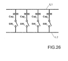
- the Integrated Circuit is in this particular case a digital capacitor bank comprising four MEMS switches (or MEMS relays) SW1, SW2, SW3, SW4 that are connected in parallel ( figure 26 ) by electrical interconnection lines IL1 and IL2 (signal lines).
- the interconnection line IL1 is embedding MEMS fixed capacitors Cap1, Cap2, Cap3, Cap4 of the invention for each switch SW1, SW2, SW3, SW4.
Landscapes
- Engineering & Computer Science (AREA)
- Power Engineering (AREA)
- Microelectronics & Electronic Packaging (AREA)
- Micromachines (AREA)
- Semiconductor Integrated Circuits (AREA)
- Mechanical Engineering (AREA)
- Computer Hardware Design (AREA)
Priority Applications (7)
| Application Number | Priority Date | Filing Date | Title |
|---|---|---|---|
| EP12306326.5A EP2725595A1 (de) | 2012-10-25 | 2012-10-25 | MEMS-Festkondensator mit einem gashaltigen Spalt und Verfahren zur Herstellung des besagten Kondensators |
| TW102138420A TW201426829A (zh) | 2012-10-25 | 2013-10-24 | 包括含有氣體之間隙的微機電系統固定電容器和用於製造該電容器的製程 |
| PCT/EP2013/072252 WO2014064185A1 (en) | 2012-10-25 | 2013-10-24 | Mems fixed capacitor comprising a gas-containing gap and process for manufacturing said capacitor |
| CN201380056250.0A CN104756212A (zh) | 2012-10-25 | 2013-10-24 | 包括含气体的间隙的mems固定电容和用于制造所述电容器的方法 |
| US14/436,274 US20150243729A1 (en) | 2012-10-25 | 2013-10-24 | Mems fixed capacitor comprising a gas-containing gap and process for manufacturing said capacitor |
| KR1020157005199A KR20150073946A (ko) | 2012-10-25 | 2013-10-24 | 가스 보유 간극을 포함하는 mems 고정 커패시터 및 이러한 커페시터를 제조하는 방법 |
| JP2015538439A JP2015535393A (ja) | 2012-10-25 | 2013-10-24 | ガス含有間隙を含むmems固定コンデンサー及び前記コンデンサーを製造するための方法 |
Applications Claiming Priority (1)
| Application Number | Priority Date | Filing Date | Title |
|---|---|---|---|
| EP12306326.5A EP2725595A1 (de) | 2012-10-25 | 2012-10-25 | MEMS-Festkondensator mit einem gashaltigen Spalt und Verfahren zur Herstellung des besagten Kondensators |
Publications (1)
| Publication Number | Publication Date |
|---|---|
| EP2725595A1 true EP2725595A1 (de) | 2014-04-30 |
Family
ID=47088772
Family Applications (1)
| Application Number | Title | Priority Date | Filing Date |
|---|---|---|---|
| EP12306326.5A Pending EP2725595A1 (de) | 2012-10-25 | 2012-10-25 | MEMS-Festkondensator mit einem gashaltigen Spalt und Verfahren zur Herstellung des besagten Kondensators |
Country Status (7)
| Country | Link |
|---|---|
| US (1) | US20150243729A1 (de) |
| EP (1) | EP2725595A1 (de) |
| JP (1) | JP2015535393A (de) |
| KR (1) | KR20150073946A (de) |
| CN (1) | CN104756212A (de) |
| TW (1) | TW201426829A (de) |
| WO (1) | WO2014064185A1 (de) |
Cited By (1)
| Publication number | Priority date | Publication date | Assignee | Title |
|---|---|---|---|---|
| TWI654793B (zh) | 2015-08-28 | 2019-03-21 | 美商通用電機股份有限公司 | 具有倒置微帶傳輸線的射頻微機電系統及其製造方法 |
Families Citing this family (2)
| Publication number | Priority date | Publication date | Assignee | Title |
|---|---|---|---|---|
| DE102015111425B4 (de) * | 2014-07-18 | 2016-06-30 | Klaus Kürschner | Verfahren und Einrichtung zur elektrischen Kraftmessung mittels Isolationsdünnschicht |
| DE102018101389A1 (de) * | 2018-01-23 | 2019-07-25 | Osram Opto Semiconductors Gmbh | Strahlungsemittierender halbleiterchip und verfahren zur herstellung eines strahlungsemittierenden halbleiterchips |
Citations (7)
| Publication number | Priority date | Publication date | Assignee | Title |
|---|---|---|---|---|
| US6437965B1 (en) | 2000-11-28 | 2002-08-20 | Harris Corporation | Electronic device including multiple capacitance value MEMS capacitor and associated methods |
| US20050248423A1 (en) * | 2004-03-12 | 2005-11-10 | The Regents Of The University Of California | High isolation tunable MEMS capacitive switch |
| WO2006063257A2 (en) | 2004-12-09 | 2006-06-15 | Wispry, Inc. | Micro-electro-mechanical system (mems) capacitors, inductors, and related systems and methods |
| US20070278075A1 (en) * | 2004-07-29 | 2007-12-06 | Akihisa Terano | Capacitance Type Mems Device, Manufacturing Method Thereof, And High Frequency Device |
| WO2009057988A2 (en) * | 2007-10-31 | 2009-05-07 | Mimos Berhad | Radio frequency mems switch |
| US20090207549A1 (en) * | 2008-02-20 | 2009-08-20 | Fujitsu Limited | Variable capacitor, matching circuit element, and mobile terminal apparatus |
| US20110128083A1 (en) * | 2009-11-27 | 2011-06-02 | Stmicroelectronics S.R.L. | Microelectromechanical resonant structure having improved electrical characteristics |
Family Cites Families (1)
| Publication number | Priority date | Publication date | Assignee | Title |
|---|---|---|---|---|
| US7657242B2 (en) * | 2004-09-27 | 2010-02-02 | Qualcomm Mems Technologies, Inc. | Selectable capacitance circuit |
-
2012
- 2012-10-25 EP EP12306326.5A patent/EP2725595A1/de active Pending
-
2013
- 2013-10-24 CN CN201380056250.0A patent/CN104756212A/zh active Pending
- 2013-10-24 US US14/436,274 patent/US20150243729A1/en not_active Abandoned
- 2013-10-24 WO PCT/EP2013/072252 patent/WO2014064185A1/en not_active Ceased
- 2013-10-24 JP JP2015538439A patent/JP2015535393A/ja active Pending
- 2013-10-24 KR KR1020157005199A patent/KR20150073946A/ko not_active Withdrawn
- 2013-10-24 TW TW102138420A patent/TW201426829A/zh unknown
Patent Citations (7)
| Publication number | Priority date | Publication date | Assignee | Title |
|---|---|---|---|---|
| US6437965B1 (en) | 2000-11-28 | 2002-08-20 | Harris Corporation | Electronic device including multiple capacitance value MEMS capacitor and associated methods |
| US20050248423A1 (en) * | 2004-03-12 | 2005-11-10 | The Regents Of The University Of California | High isolation tunable MEMS capacitive switch |
| US20070278075A1 (en) * | 2004-07-29 | 2007-12-06 | Akihisa Terano | Capacitance Type Mems Device, Manufacturing Method Thereof, And High Frequency Device |
| WO2006063257A2 (en) | 2004-12-09 | 2006-06-15 | Wispry, Inc. | Micro-electro-mechanical system (mems) capacitors, inductors, and related systems and methods |
| WO2009057988A2 (en) * | 2007-10-31 | 2009-05-07 | Mimos Berhad | Radio frequency mems switch |
| US20090207549A1 (en) * | 2008-02-20 | 2009-08-20 | Fujitsu Limited | Variable capacitor, matching circuit element, and mobile terminal apparatus |
| US20110128083A1 (en) * | 2009-11-27 | 2011-06-02 | Stmicroelectronics S.R.L. | Microelectromechanical resonant structure having improved electrical characteristics |
Cited By (1)
| Publication number | Priority date | Publication date | Assignee | Title |
|---|---|---|---|---|
| TWI654793B (zh) | 2015-08-28 | 2019-03-21 | 美商通用電機股份有限公司 | 具有倒置微帶傳輸線的射頻微機電系統及其製造方法 |
Also Published As
| Publication number | Publication date |
|---|---|
| JP2015535393A (ja) | 2015-12-10 |
| US20150243729A1 (en) | 2015-08-27 |
| CN104756212A (zh) | 2015-07-01 |
| KR20150073946A (ko) | 2015-07-01 |
| WO2014064185A1 (en) | 2014-05-01 |
| TW201426829A (zh) | 2014-07-01 |
Similar Documents
| Publication | Publication Date | Title |
|---|---|---|
| KR101268208B1 (ko) | 높은 캐패시턴스 rf mems 스위치들을 제공하기 위한 시스템 및 방법 | |
| DE112011102124T9 (de) | Mikroelektromechanisches System | |
| US8503157B2 (en) | MEMS device | |
| US8022599B2 (en) | Actuator | |
| US7141989B1 (en) | Methods and apparatus for a MEMS varactor | |
| US7489004B2 (en) | Micro-electro-mechanical variable capacitor for radio frequency applications with reduced influence of a surface roughness | |
| WO2001061848A1 (en) | A micromechanical tunable capacitor and an integrated tunable resonator | |
| EP3723148A1 (de) | Dreidimensionale kapazitive strukturen und deren herstellungsverfahren | |
| EP2725595A1 (de) | MEMS-Festkondensator mit einem gashaltigen Spalt und Verfahren zur Herstellung des besagten Kondensators | |
| US7297571B2 (en) | Electrostatically actuated low response time power commutation micro-switches | |
| EP3796351B1 (de) | Fehlerarmer dünner festelektrolytkondensator mit hoher kapazität und verfahren zur herstellung davon | |
| HK1194198A (en) | Mems fixed capacitor comprising a gas-containing gap and process for manufacturing said capacitor | |
| CN102422373B (zh) | 具有格栅作为中间电极的rf mems开关 | |
| CN100521030C (zh) | 微机电装置和模块及其驱动方法 | |
| Choi et al. | Increasing Capacitance and Self-Resonant Frequency of the MEMS Switched Capacitor Using High-$\kappa $ TiO 2 and SU-8 Bridged Beam Structure | |
| US6421224B1 (en) | Micro-structure capacitor | |
| US8059385B2 (en) | Substrates with slotted metals and related methods | |
| Pu et al. | Stable zipping RF MEMS varactors | |
| US7218191B2 (en) | Micro-electro mechanical switch designs | |
| Ramli et al. | Design and modelling of a digital MEMS varactor for wireless applications | |
| CN121399711A (zh) | Mems桥 | |
| CN120236905A (zh) | 多层电子组件 | |
| CN120221282A (zh) | 多层电子组件 | |
| Bakri-Kassem et al. | A parallel-plate MEMS variable capacitor with vertical thin-film comb actuators | |
| CN120236888A (zh) | 多层电子组件 |
Legal Events
| Date | Code | Title | Description |
|---|---|---|---|
| PUAI | Public reference made under article 153(3) epc to a published international application that has entered the european phase |
Free format text: ORIGINAL CODE: 0009012 |
|
| 17P | Request for examination filed |
Effective date: 20121025 |
|
| AK | Designated contracting states |
Kind code of ref document: A1 Designated state(s): AL AT BE BG CH CY CZ DE DK EE ES FI FR GB GR HR HU IE IS IT LI LT LU LV MC MK MT NL NO PL PT RO RS SE SI SK SM TR |
|
| AX | Request for extension of the european patent |
Extension state: BA ME |
|
| REG | Reference to a national code |
Ref country code: HK Ref legal event code: DE Ref document number: 1194198 Country of ref document: HK |
|
| 17P | Request for examination filed |
Effective date: 20141014 |
|
| RBV | Designated contracting states (corrected) |
Designated state(s): AL AT BE BG CH CY CZ DE DK EE ES FI FR GB GR HR HU IE IS IT LI LT LU LV MC MK MT NL NO PL PT RO RS SE SI SK SM TR |
|
| 17Q | First examination report despatched |
Effective date: 20150209 |
|
| GRAP | Despatch of communication of intention to grant a patent |
Free format text: ORIGINAL CODE: EPIDOSNIGR1 |
|
| INTG | Intention to grant announced |
Effective date: 20151008 |
|
| 19U | Interruption of proceedings before grant |
Effective date: 20160203 |
|
| REG | Reference to a national code |
Ref country code: HK Ref legal event code: WD Ref document number: 1194198 Country of ref document: HK |
|
| 19W | Proceedings resumed before grant after interruption of proceedings |
Effective date: 20211001 |
|
| PUAJ | Public notification under rule 129 epc |
Free format text: ORIGINAL CODE: 0009425 |
|
| 32PN | Public notification |
Free format text: COMMUNICATION PURSUANT TO RULE 142 EPC (RESUMPTION OF PROCEEDINGS UNDER RULE 142(2) EPC DATED 16.04.2021) |
|
| STAA | Information on the status of an ep patent application or granted ep patent |
Free format text: STATUS: GRANT OF PATENT IS INTENDED |
|
| STAA | Information on the status of an ep patent application or granted ep patent |
Free format text: STATUS: THE APPLICATION IS DEEMED TO BE WITHDRAWN |
|
| PUAJ | Public notification under rule 129 epc |
Free format text: ORIGINAL CODE: 0009425 |
|
| STAA | Information on the status of an ep patent application or granted ep patent |
Free format text: STATUS: GRANT OF PATENT IS INTENDED |
|
| 18D | Application deemed to be withdrawn |
Effective date: 20220201 |
|
| 32PN | Public notification |
Free format text: NOTING OF LOSS OF RIGHTS PURSUANT TO RULE 112(1) EPC (EPO FORM 2015C DATED 22.04.2024) |
|
| D18D | Application deemed to be withdrawn (deleted) | ||
| STAA | Information on the status of an ep patent application or granted ep patent |
Free format text: STATUS: THE APPLICATION IS DEEMED TO BE WITHDRAWN |
|
| R18D | Application deemed to be withdrawn (corrected) |
Effective date: 20220201 |