EP2728510B1 - Dispositif NFC et procédé de communication - Google Patents
Dispositif NFC et procédé de communication Download PDFInfo
- Publication number
- EP2728510B1 EP2728510B1 EP12191425.3A EP12191425A EP2728510B1 EP 2728510 B1 EP2728510 B1 EP 2728510B1 EP 12191425 A EP12191425 A EP 12191425A EP 2728510 B1 EP2728510 B1 EP 2728510B1
- Authority
- EP
- European Patent Office
- Prior art keywords
- nfc
- detuning
- nfc device
- antenna unit
- transistor
- Prior art date
- Legal status (The legal status is an assumption and is not a legal conclusion. Google has not performed a legal analysis and makes no representation as to the accuracy of the status listed.)
- Active
Links
Images


Classifications
-
- H—ELECTRICITY
- H04—ELECTRIC COMMUNICATION TECHNIQUE
- H04B—TRANSMISSION
- H04B5/00—Near-field transmission systems, e.g. inductive or capacitive transmission systems
- H04B5/70—Near-field transmission systems, e.g. inductive or capacitive transmission systems specially adapted for specific purposes
- H04B5/77—Near-field transmission systems, e.g. inductive or capacitive transmission systems specially adapted for specific purposes for interrogation
-
- G—PHYSICS
- G06—COMPUTING OR CALCULATING; COUNTING
- G06K—GRAPHICAL DATA READING; PRESENTATION OF DATA; RECORD CARRIERS; HANDLING RECORD CARRIERS
- G06K7/00—Methods or arrangements for sensing record carriers, e.g. for reading patterns
- G06K7/0008—General problems related to the reading of electronic memory record carriers, independent of its reading method, e.g. power transfer
-
- G—PHYSICS
- G06—COMPUTING OR CALCULATING; COUNTING
- G06K—GRAPHICAL DATA READING; PRESENTATION OF DATA; RECORD CARRIERS; HANDLING RECORD CARRIERS
- G06K19/00—Record carriers for use with machines and with at least a part designed to carry digital markings
- G06K19/06—Record carriers for use with machines and with at least a part designed to carry digital markings characterised by the kind of the digital marking, e.g. shape, nature, code
- G06K19/067—Record carriers with conductive marks, printed circuits or semiconductor circuit elements, e.g. credit or identity cards also with resonating or responding marks without active components
- G06K19/07—Record carriers with conductive marks, printed circuits or semiconductor circuit elements, e.g. credit or identity cards also with resonating or responding marks without active components with integrated circuit chips
- G06K19/0723—Record carriers with conductive marks, printed circuits or semiconductor circuit elements, e.g. credit or identity cards also with resonating or responding marks without active components with integrated circuit chips the record carrier comprising an arrangement for non-contact communication, e.g. wireless communication circuits on transponder cards, non-contact smart cards or RFIDs
-
- G—PHYSICS
- G06—COMPUTING OR CALCULATING; COUNTING
- G06K—GRAPHICAL DATA READING; PRESENTATION OF DATA; RECORD CARRIERS; HANDLING RECORD CARRIERS
- G06K7/00—Methods or arrangements for sensing record carriers, e.g. for reading patterns
- G06K7/10—Methods or arrangements for sensing record carriers, e.g. for reading patterns by electromagnetic radiation, e.g. optical sensing; by corpuscular radiation
- G06K7/10009—Methods or arrangements for sensing record carriers, e.g. for reading patterns by electromagnetic radiation, e.g. optical sensing; by corpuscular radiation sensing by radiation using wavelengths larger than 0.1 mm, e.g. radio-waves or microwaves
- G06K7/10118—Methods or arrangements for sensing record carriers, e.g. for reading patterns by electromagnetic radiation, e.g. optical sensing; by corpuscular radiation sensing by radiation using wavelengths larger than 0.1 mm, e.g. radio-waves or microwaves the sensing being preceded by at least one preliminary step
- G06K7/10148—Methods or arrangements for sensing record carriers, e.g. for reading patterns by electromagnetic radiation, e.g. optical sensing; by corpuscular radiation sensing by radiation using wavelengths larger than 0.1 mm, e.g. radio-waves or microwaves the sensing being preceded by at least one preliminary step the step consisting of dynamically tuning the resonant circuit of the interrogation device that is emitting the interrogation signal, e.g. for impedance matching inside of the interrogation device
-
- G—PHYSICS
- G06—COMPUTING OR CALCULATING; COUNTING
- G06K—GRAPHICAL DATA READING; PRESENTATION OF DATA; RECORD CARRIERS; HANDLING RECORD CARRIERS
- G06K7/00—Methods or arrangements for sensing record carriers, e.g. for reading patterns
- G06K7/10—Methods or arrangements for sensing record carriers, e.g. for reading patterns by electromagnetic radiation, e.g. optical sensing; by corpuscular radiation
- G06K7/10009—Methods or arrangements for sensing record carriers, e.g. for reading patterns by electromagnetic radiation, e.g. optical sensing; by corpuscular radiation sensing by radiation using wavelengths larger than 0.1 mm, e.g. radio-waves or microwaves
- G06K7/10237—Methods or arrangements for sensing record carriers, e.g. for reading patterns by electromagnetic radiation, e.g. optical sensing; by corpuscular radiation sensing by radiation using wavelengths larger than 0.1 mm, e.g. radio-waves or microwaves the reader and the record carrier being capable of selectively switching between reader and record carrier appearance, e.g. in near field communication [NFC] devices where the NFC device may function as an RFID reader or as an RFID tag
Definitions
- the invention relates to an NFC device for communicating with an NFC reader.
- the invention also relates to a cover comprising an NFC device.
- the invention further relates to a method of communication between an NFC device and an NFC reader.
- NFC-enabled mobile phones have become increasingly popular. Also, phone sleeves or covers for such mobile phones have entered the market. These covers can be equipped with integrated sensors which are able to measure physical phenomena, such as temperature, humidity and pressure. The sensors produce measurement results that are sent from the cover to the mobile device, which is typically done via electrical connections between the cover and the mobile phone. For example, this can be done via a docking plug of the mobile phone. Subsequently, the measurement results can be processed by the mobile phone. However, creating electrical connections between the cover and the mobile phone is cumbersome and expensive.
- a system includes a first interface, a second interface, secure memory, a user-interface module, a processing module, and an amplification module.
- the first interface connects to a microSD slot of a mobile host device.
- the second interface includes an internal antenna for wirelessly communicating with retail terminals.
- the secure memory stores user credentials and a payment application used to execute financial transactions with the retail terminals.
- the processing module executes the payment application using the user credentials in response to at least a transaction request received by the RF module and transmits at least one transaction response to the retail terminal based, at least in part, on the executed payment application.
- the amplification module is connected to a lead of the antenna and is configured to amplify at least received RF signals.
- NFC-enabled mobile device Since an NFC-enabled mobile device is always equipped with an NFC reader, it is possible, in principle, to embed an NFC device (NFC tag) in the cover and to transmit data from the cover to the mobile device via near-field communication.
- NFC requires that an NFC device repeatedly leaves and re-enters the field generated by the NFC reader in order to transmit data to said reader in a periodic fashion. This is not the case if the mobile device is kept within the cover all the time, because then the NFC device and the NFC reader remain within communication range of each other.
- a detuning circuit within the NFC device causes a periodic detuning of the antenna unit to a detuned state, such that data transmission between the NFC device and the NFC reader may take place periodically while the NFC device and the NFC reader remain within communication range of each other. Only when the antenna unit is not in the detuned state, data transmission is possible between the NFC device and the NFC reader. Thus, a repeated leaving and re-entering the field generated by the NFC reader is simulated by a periodic detuning of the antenna unit.
- an NFC device for communicating with an NFC reader comprising an NFC integrated circuit, an antenna unit connected to said NFC integrated circuit, and a detuning circuit, wherein the detuning circuit is arranged to cause a periodic detuning of the antenna unit to a detuned state, such that data transmission between the NFC device and the NFC reader may take place periodically while the NFC device and the NFC reader remain within communication range of each other.
- the detuning circuit is arranged to receive a detuning signal from a processing unit comprised in said NFC device, and the detuning circuit is arranged to detune the antenna unit in response to receiving said detuning signal.
- the detuning circuit causes said periodic detuning of the antenna unit to a detuned state by periodically short-circuiting a coil of said antenna unit.
- the detuning circuit comprises a first capacitor connected to a tuning capacitance and to a first input of the antenna unit, a second capacitor connected to a second input of the antenna unit, a first transistor connected to the first capacitor and to ground, a second transistor connected to the second capacitor and to ground, wherein the base of the first transistor and the base of the second transistor are connected to an output of the processing unit via a first resistor and a second resistor, respectively, such that the first transistor and the second transistor are arranged to be activated by the detuning signal from the processing unit, thereby enabling said short-circuiting of the coil of the antenna unit.
- the antenna unit is in the detuned state when it has an operating frequency that substantially deviates from 13.56 MHz.
- a cover which comprises an NFC device of the kind set forth, wherein said cover is arranged to accommodate a mobile device comprising said NFC reader.
- said cover comprises at least one sensor which is arranged to measure one or more physical phenomena, and the NFC device is arranged to transmit measurement results produced by said sensor to the NFC reader when the antenna unit is not in the detuned state.
- a method of communication between an NFC device and an NFC reader comprising an NFC integrated circuit, an antenna unit connected to said NFC integrated circuit, and a detuning circuit, wherein the detuning circuit causes a periodic detuning of the antenna unit to a detuned state, such that data transmission between the NFC device and the NFC reader takes place periodically while the NFC device and the NFC reader remain within communication range of each other.
- Fig. 1 shows a portion of a conventional NFC device.
- the NFC device 100 comprises an NFC integrated circuit 102, an antenna unit 104 and a tuning capacitance 106.
- the tuning capacitance 106 is relatively small and it is used to tune the coil of the antenna unit exactly to an operating frequency of 13.56 MHz.
- Fig. 2 shows a portion of an NFC device according to an exemplary embodiment of the invention.
- the NFC device 100 according to this exemplary embodiment has been extended with a detuning circuit 200.
- the detuning circuit 200 is arranged to cause a periodic detuning of the antenna unit 104 under control of a detuning signal NFC_DEAD.
- the detuning circuit 200 comprises a first capacitor 202 connected to the tuning capacitance 106 of the NFC device 100 and to a first input of the antenna unit 104, a second capacitor 204 connected to a second input of the antenna unit 104, a first transistor 206 connected to the first capacitor 202 and to ground GND, a second transistor 208 connected to the second capacitor 204 and to ground GND.
- the detuning signal NFC_DEAD is fed to the base of the first transistor 206 and the base of the second transistor 208 via a first resistor 201 and a second resistor 212, respectively. If the detuning signal NFC_DEAD goes high, then the first transistor 206 and the second transistor 208 will be activated and, as a consequence, the coil of the antenna unit 104 will be short-circuited to ground GND.
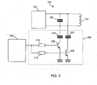
- Fig. 3 shows a portion of a system comprising an NFC device according to an exemplary embodiment of the invention.
- This system may form part of a cover which accommodates an NFC-enabled mobile phone, for example.
- the system comprises the NFC device 100 extended with the detuning circuit 200 and a processing unit 300.
- the processing unit 300 is arranged to generate and output the detuning signal NFC_DEAD.
- the processing unit 300 may be implemented as microcontroller, for example.
- the transistors 206, 208 may be implemented as field-effect transistors (FETs), for example.
- the transistors In operation, when the detuning signal NFC_DEAD is high, the transistors will conduct and basically the coil is shorted to ground by the low RDSon FET resistance, making it invisible for an NFC reader on 13.56 MHz.
- the detuning signal NFC_DEAD is low again, a rest capacitance is left because of the output capacity of the transistors. This rest capacitance can partly take over the role of the tuning capacitance 106. In fact, the tuning capacitance 106 may in principle be omitted.
- the first capacitor 202 and the second capacitor 204 are relatively large in comparison with the transistor capacitance (when open) so they do not have a frequency influence, but they can short the coil when the transistors are closed.
- the elegancy of this solution is that there are no switching components needed in series with the coil. This avoids a deterioration of the quality of the coil and makes easy switching with respect to ground possible.
- the NFC field from the reader is still strong enough to penetrate the cover.
- other NFC devices tags
- Fig. 4 shows a printed circuit board (PCB) design according to an exemplary embodiment of the invention.
- the NFC device 100 extended with the detuning circuit 102 is shown in a first oval 400.
- the antenna unit 104 is clearly visible in a first rectangle 404 in the center of the PCB.
- the processing unit 300 is visible in a second oval 402 on the PCB.
- Sensors are integrated on the right side of the PCB in a second rectangle 406.
- the position of a coil in a mobile phone which must be aligned with the position of the coil in a cover in order to enable proper communication, may differ per phone brand.
- the position of the coil is such that it is compatible with the PCB design as shown in Fig. 4 .
- the antenna unit 104 may be positioned differently in accordance with the constraints imposed by the design of the phone.
- the on-board microcontroller 300 - in this case a LPC11U14 processor produced by NXP Semiconductors - controls the detuning signal NFC_DEAD in order to trigger an NFC transaction with the phone.
- An NFC transaction is triggered by making the detuning signal NFC_DEAD low.
- Sensors temperature and pressure
- RTC real-time clock
- the low-power design consumes only a few ⁇ A while in deep-sleep mode.
- the battery is charged from the NFC field (with a second coil, not shown). Based on the RTC - that is used as a timer device - the NFC device 100 is woken up, the sensor measurements are performed and the NFC transaction is triggered.
- the on-board processor 300 can write/read data to/from the NFC device 100 via the Universal Asynchronous Receiver/Transmitter (UART) interface of the processor.
- UART Universal Asynchronous Receiver/Transmitter
- the NFC tag has a wired connection to the host device (processor), so it is in fact a so-called "Connected Tag".
- the mobile phone can write/read data to/from the NFC device 100 via the wireless NFC connection.
- any reference sign placed between parentheses shall not be construed as limiting the claim.
- the word “comprise(s)” or “comprising” does not exclude the presence of elements or steps other than those listed in a claim.
- the word “a” or “an” preceding an element does not exclude the presence of a plurality of such elements.
- the invention may be implemented by means of hardware comprising several distinct elements and/or by means of a suitably programmed processor. In a device claim enumerating several means, several of these means may be embodied by one and the same item of hardware.
- the mere fact that certain measures are recited in mutually different dependent claims does not indicate that a combination of these measures cannot be used to advantage.
Landscapes
- Engineering & Computer Science (AREA)
- Physics & Mathematics (AREA)
- Health & Medical Sciences (AREA)
- Toxicology (AREA)
- Theoretical Computer Science (AREA)
- General Physics & Mathematics (AREA)
- Artificial Intelligence (AREA)
- Computer Vision & Pattern Recognition (AREA)
- General Health & Medical Sciences (AREA)
- Electromagnetism (AREA)
- Computer Networks & Wireless Communication (AREA)
- Computer Hardware Design (AREA)
- Microelectronics & Electronic Packaging (AREA)
- Signal Processing (AREA)
- Near-Field Transmission Systems (AREA)
Claims (8)
- Dispositif NFC (100) destiné à communiquer avec un lecteur NFC, le dispositif NFC (100) comprenant un circuit intégré NFC (102) et une unité antenne (104) reliée audit circuit intégré NFC (102), le dispositif NFC (100) étant caractérisé en ce qu'il comprend en outre un circuit de désaccord (200), lequel circuit de désaccord (200) est conçu pour provoquer un désaccord périodique de l'unité antenne (104) pour lui faire adopter un état désaccordé, de façon à permettre une transmission de données périodique entre le dispositif NFC (100) et le lecteur NFC tandis que le dispositif NFC (100) et le lecteur NFC restent à portée de communication l'un de l'autre.
- Dispositif NFC (100) selon la revendication 1, dans lequel le circuit de désaccord (200) est conçu pour recevoir un signal de désaccord (NFC_DEAD) en provenance d'une unité de traitement (300) contenue dans ledit dispositif NFC (100), et dans lequel le circuit de désaccord (200) est conçu pour désaccorder l'unité antenne (104) en réponse à la réception dudit signal de désaccord (NFC_DEAD).
- Dispositif NFC (100) selon la revendication 1 ou 2, dans lequel le circuit de désaccord (200) provoque ledit désaccord périodique de l'unité antenne (104) pour lui faire adopter un état désaccordé par court-circuitage périodique d'une bobine de ladite unité antenne (104).
- Dispositif NFC (100) selon la revendication 3, dans lequel le circuit de désaccord (200) comprend un premier condensateur (202) relié à un condensateur d'accord (106) et à une première entrée de l'unité antenne (104), un deuxième condensateur (204) relié à une deuxième entrée de l'unité antenne (104), un premier transistor (206) relié au premier condensateur (202) et à la masse (GND), un deuxième transistor (208) relié au deuxième condensateur (204) et à la masse (GND), la base du premier transistor (206) et la base du deuxième transistor (208) étant reliées à une sortie de l'unité de traitement (300) par le biais respectivement d'une première résistance (201) et d'une deuxième résistance (212) de façon à ce que le premier transistor (206) et le deuxième transistor (208) puissent être activés par le signal de désaccord (NFC_DEAD) à partir de l'unité de traitement (300) en permettant ainsi ledit court-circuitage de la bobine de l'unité antenne (104).
- Dispositif NFC (100) selon l'une quelconque des revendications précédentes, dans lequel l'unité antenne (104) occupe l'état désaccordé lorsque sa fréquence de fonctionnement s'écarte sensiblement de 13,56 MHz.
- Coque comprenant un dispositif NFC (100) selon l'une quelconque des revendications précédentes, laquelle coque est conçue pour accueillir un dispositif mobile comprenant ledit lecteur NFC.
- Coque selon la revendication 6, laquelle coque comprend au moins un capteur conçu pour mesurer un ou plusieurs phénomènes physiques, et le dispositif NFC (100) étant conçu pour transmettre des résultats de mesure produits par ledit capteur au lecteur NFC lorsque l'unité antenne (104) n'occupe pas l'état désaccordé.
- Procédé de communication entre un dispositif NFC (100) et un lecteur NFC, le dispositif NFC (100) comprenant un circuit intégré NFC (102) et une unité antenne (104) reliée audit circuit intégré NFC (102), le procédé étant caractérisé en ce que le dispositif NFC (100) comprend en outre un circuit de désaccord (200), lequel circuit de désaccord (200) provoque un désaccord périodique de l'unité antenne (104) pour lui faire adopter un état désaccordé, de façon à permettre une transmission de données périodique entre le dispositif NFC (100) et le lecteur NFC tandis que le dispositif NFC (100) et le lecteur NFC restent à portée de communication l'un de l'autre.
Priority Applications (2)
| Application Number | Priority Date | Filing Date | Title |
|---|---|---|---|
| EP12191425.3A EP2728510B1 (fr) | 2012-11-06 | 2012-11-06 | Dispositif NFC et procédé de communication |
| US14/072,736 US9236914B2 (en) | 2012-11-06 | 2013-11-05 | NFC device and communication method |
Applications Claiming Priority (1)
| Application Number | Priority Date | Filing Date | Title |
|---|---|---|---|
| EP12191425.3A EP2728510B1 (fr) | 2012-11-06 | 2012-11-06 | Dispositif NFC et procédé de communication |
Publications (2)
| Publication Number | Publication Date |
|---|---|
| EP2728510A1 EP2728510A1 (fr) | 2014-05-07 |
| EP2728510B1 true EP2728510B1 (fr) | 2015-04-15 |
Family
ID=47177790
Family Applications (1)
| Application Number | Title | Priority Date | Filing Date |
|---|---|---|---|
| EP12191425.3A Active EP2728510B1 (fr) | 2012-11-06 | 2012-11-06 | Dispositif NFC et procédé de communication |
Country Status (2)
| Country | Link |
|---|---|
| US (1) | US9236914B2 (fr) |
| EP (1) | EP2728510B1 (fr) |
Families Citing this family (33)
| Publication number | Priority date | Publication date | Assignee | Title |
|---|---|---|---|---|
| US8612352B2 (en) | 2010-10-13 | 2013-12-17 | Square, Inc. | Decoding systems with a decoding engine running on a mobile device and coupled to a payment system that includes identifying information of second parties qualified to conduct business with the payment system |
| US9058172B2 (en) | 2012-07-02 | 2015-06-16 | Square, Inc. | Method for conserving power using a wireless card reader |
| EP2779671B1 (fr) | 2013-03-11 | 2017-12-13 | Nagravision S.A. | Support électronique permettant l'accès audio/vidéo à distance |
| WO2015004112A1 (fr) | 2013-07-11 | 2015-01-15 | Styrolution Group Gmbh | Procédé pour réaliser des matieres a mouler thermoplastiques et matieres a mouler thermoplastiques ainsi réalisées |
| EP3032836A1 (fr) * | 2014-12-12 | 2016-06-15 | SmarDTV S.A. | Système de fourniture d'accès à un contenu multimédia à accès conditionnel |
| US9396368B1 (en) | 2015-05-23 | 2016-07-19 | Square, Inc. | Tuning a NFC antenna of a device |
| US10182328B1 (en) | 2015-05-23 | 2019-01-15 | Square, Inc. | Point of sale (POS) device responsive to detected interference with antenna |
| US10318952B1 (en) | 2015-05-23 | 2019-06-11 | Square, Inc. | NFC base station and passive transmitter device |
| USD766901S1 (en) | 2015-05-29 | 2016-09-20 | Square, Inc. | Card reader |
| USD766238S1 (en) | 2015-05-29 | 2016-09-13 | Square, Inc. | Card reader |
| US11023878B1 (en) | 2015-06-05 | 2021-06-01 | Square, Inc. | Apparatuses, methods, and systems for transmitting payment proxy information |
| US10482440B1 (en) | 2015-09-18 | 2019-11-19 | Square, Inc. | Simulating NFC experience |
| US10861003B1 (en) | 2015-09-24 | 2020-12-08 | Square, Inc. | Near field communication device coupling system |
| US9646299B1 (en) | 2015-09-25 | 2017-05-09 | Square, Inc. | Dynamic adjustment of near field communication tuning parameters |
| US10198727B1 (en) | 2015-09-25 | 2019-02-05 | Square, Inc. | Modulation of a near-field communication signal |
| US10955977B2 (en) | 2015-11-03 | 2021-03-23 | Microsoft Technology Licensing, Llc | Extender object for multi-modal sensing |
| US10649572B2 (en) * | 2015-11-03 | 2020-05-12 | Microsoft Technology Licensing, Llc | Multi-modal sensing surface |
| US10338753B2 (en) | 2015-11-03 | 2019-07-02 | Microsoft Technology Licensing, Llc | Flexible multi-layer sensing surface |
| US9721123B1 (en) | 2015-12-11 | 2017-08-01 | Square, Inc. | Microcontroller intercept of EMV card contact switch |
| US10366383B2 (en) | 2016-03-31 | 2019-07-30 | Square, Inc. | Combined reliable and unreliable data transmission |
| US9542678B1 (en) | 2016-03-31 | 2017-01-10 | Square, Inc. | Exclusive bonding of wireless devices |
| US10402816B2 (en) | 2016-12-31 | 2019-09-03 | Square, Inc. | Partial data object acquisition and processing |
| US10621590B2 (en) | 2017-02-22 | 2020-04-14 | Square, Inc. | Line-based chip card tamper detection |
| US10438189B2 (en) | 2017-02-22 | 2019-10-08 | Square, Inc. | Server-enabled chip card interface tamper detection |
| US10579566B2 (en) | 2017-04-28 | 2020-03-03 | Square, Inc. | Point of sale device with switchable internal connection roles |
| US10733589B2 (en) | 2017-04-28 | 2020-08-04 | Square, Inc. | Point of sale device power management and under voltage protection |
| US10430784B1 (en) | 2017-08-31 | 2019-10-01 | Square, Inc. | Multi-layer antenna |
| US10455392B2 (en) | 2017-09-27 | 2019-10-22 | Apple Inc. | Adaptive matching with antenna detuning detection |
| US11257058B1 (en) * | 2017-10-30 | 2022-02-22 | Square, Inc. | Sharing output device between unsecured processor and secured processor |
| US10970698B1 (en) * | 2017-12-08 | 2021-04-06 | Square, Inc. | Reader detection signal bypassing secure processor |
| US10708407B2 (en) | 2018-12-10 | 2020-07-07 | Google Llc | Mobile device case equipped for short-range communication with a mobile device |
| US11182770B1 (en) | 2018-12-12 | 2021-11-23 | Square, Inc. | Systems and methods for sensing locations of near field communication devices |
| GB202014141D0 (en) * | 2020-09-09 | 2020-10-21 | Ifpl Group Ltd | Contactless reader |
Family Cites Families (4)
| Publication number | Priority date | Publication date | Assignee | Title |
|---|---|---|---|---|
| US8915447B2 (en) * | 2007-09-12 | 2014-12-23 | Devicefidelity, Inc. | Amplifying radio frequency signals |
| US20090152364A1 (en) * | 2007-12-12 | 2009-06-18 | Spivey Technologies, Llc | Rfid card with piezoelectric element |
| US9923587B2 (en) * | 2012-05-18 | 2018-03-20 | Blackberry Limited | Mobile wireless communications system including NFC carrying case and related methods |
| US8934837B2 (en) * | 2013-01-03 | 2015-01-13 | Blackberry Limited | Mobile wireless communications device including NFC antenna matching control circuit and associated methods |
-
2012
- 2012-11-06 EP EP12191425.3A patent/EP2728510B1/fr active Active
-
2013
- 2013-11-05 US US14/072,736 patent/US9236914B2/en active Active
Also Published As
| Publication number | Publication date |
|---|---|
| US9236914B2 (en) | 2016-01-12 |
| EP2728510A1 (fr) | 2014-05-07 |
| US20140127995A1 (en) | 2014-05-08 |
Similar Documents
| Publication | Publication Date | Title |
|---|---|---|
| EP2728510B1 (fr) | Dispositif NFC et procédé de communication | |
| US9413430B2 (en) | Measurement and reporting of received signal strength in NFC enabled devices | |
| CN104253634B (zh) | 双频多协议多功能近场通信集成系统和应用方法 | |
| US10430622B2 (en) | RFID tag with reconfigurable properties and/or reconfiguring capability | |
| US10148321B2 (en) | Antenna for near field communication, accessory and electronic device including the same | |
| WO2010022687A1 (fr) | Procédé et système de communication rf pour contrôler la distance de communication d'une carte sim rf à l'aide d'un identificateur d'étiquette | |
| CN113497641B (zh) | 通信装置和操作方法 | |
| US20130084798A1 (en) | Single nfc device identity selection on a multiple-identity supported device | |
| WO2011140458A3 (fr) | Couplage magnétique d'antennes radiofréquence | |
| US11601791B2 (en) | Method for pairing devices using near field communication and electronic apparatus using same | |
| WO2008132269A1 (fr) | Communication à courte portée | |
| US9767328B2 (en) | Autonomous tuning method to improve radio frequency performance | |
| KR20040091140A (ko) | 휴대용 디바이스 | |
| CN104361372A (zh) | 一种基于远程控制的射频卡 | |
| US11671834B2 (en) | Electronic device for transmitting/receiving data and method thereof | |
| EP3016342B1 (fr) | Dispositif mobile, procédé permettant de faciliter une transaction, programme informatique, article de fabrication | |
| EP3093799A1 (fr) | Transpondeur rfid, système à transpondeur rfid et procédé de communication entre un transpondeur rfid et un dispositif de lecture | |
| CN204557497U (zh) | 双频智能射频识别集成系统 | |
| CN203299867U (zh) | 用于检测仪器设备状态的电子标签及电子标签检测系统 | |
| CN102136855B (zh) | 一种寻找手机的系统及其方法 | |
| KR101343138B1 (ko) | 무선 태그 리더의 신뢰성 시험 장치 | |
| EP2797025B1 (fr) | Dispositif de couplage de proximité mobile comportant un affichage | |
| CN202306575U (zh) | 射频sim卡非接触读卡距离的校准设备 | |
| EP2797024B1 (fr) | Dispositif de couplage de proximité mobile | |
| KR101391079B1 (ko) | 직렬 통신 프로토콜을 이용한 rfid 리더, rfid 태그, rfid 통신 방법 및 시스템 |
Legal Events
| Date | Code | Title | Description |
|---|---|---|---|
| PUAI | Public reference made under article 153(3) epc to a published international application that has entered the european phase |
Free format text: ORIGINAL CODE: 0009012 |
|
| 17P | Request for examination filed |
Effective date: 20131031 |
|
| AK | Designated contracting states |
Kind code of ref document: A1 Designated state(s): AL AT BE BG CH CY CZ DE DK EE ES FI FR GB GR HR HU IE IS IT LI LT LU LV MC MK MT NL NO PL PT RO RS SE SI SK SM TR |
|
| AX | Request for extension of the european patent |
Extension state: BA ME |
|
| GRAJ | Information related to disapproval of communication of intention to grant by the applicant or resumption of examination proceedings by the epo deleted |
Free format text: ORIGINAL CODE: EPIDOSDIGR1 |
|
| GRAP | Despatch of communication of intention to grant a patent |
Free format text: ORIGINAL CODE: EPIDOSNIGR1 |
|
| GRAP | Despatch of communication of intention to grant a patent |
Free format text: ORIGINAL CODE: EPIDOSNIGR1 |
|
| RBV | Designated contracting states (corrected) |
Designated state(s): AL AT BE BG CH CY CZ DE DK EE ES FI FR GB GR HR HU IE IS IT LI LT LU LV MC MK MT NL NO PL PT RO RS SE SI SK SM TR |
|
| INTG | Intention to grant announced |
Effective date: 20141217 |
|
| GRAS | Grant fee paid |
Free format text: ORIGINAL CODE: EPIDOSNIGR3 |
|
| GRAA | (expected) grant |
Free format text: ORIGINAL CODE: 0009210 |
|
| AK | Designated contracting states |
Kind code of ref document: B1 Designated state(s): AL AT BE BG CH CY CZ DE DK EE ES FI FR GB GR HR HU IE IS IT LI LT LU LV MC MK MT NL NO PL PT RO RS SE SI SK SM TR |
|
| REG | Reference to a national code |
Ref country code: GB Ref legal event code: FG4D Ref country code: CH Ref legal event code: EP |
|
| REG | Reference to a national code |
Ref country code: IE Ref legal event code: FG4D |
|
| REG | Reference to a national code |
Ref country code: AT Ref legal event code: REF Ref document number: 722342 Country of ref document: AT Kind code of ref document: T Effective date: 20150515 |
|
| REG | Reference to a national code |
Ref country code: DE Ref legal event code: R096 Ref document number: 602012006676 Country of ref document: DE Effective date: 20150528 |
|
| REG | Reference to a national code |
Ref country code: NL Ref legal event code: VDEP Effective date: 20150415 |
|
| REG | Reference to a national code |
Ref country code: AT Ref legal event code: MK05 Ref document number: 722342 Country of ref document: AT Kind code of ref document: T Effective date: 20150415 |
|
| REG | Reference to a national code |
Ref country code: LT Ref legal event code: MG4D |
|
| PG25 | Lapsed in a contracting state [announced via postgrant information from national office to epo] |
Ref country code: NL Free format text: LAPSE BECAUSE OF FAILURE TO SUBMIT A TRANSLATION OF THE DESCRIPTION OR TO PAY THE FEE WITHIN THE PRESCRIBED TIME-LIMIT Effective date: 20150415 |
|
| REG | Reference to a national code |
Ref country code: FR Ref legal event code: PLFP Year of fee payment: 4 |
|
| PG25 | Lapsed in a contracting state [announced via postgrant information from national office to epo] |
Ref country code: LT Free format text: LAPSE BECAUSE OF FAILURE TO SUBMIT A TRANSLATION OF THE DESCRIPTION OR TO PAY THE FEE WITHIN THE PRESCRIBED TIME-LIMIT Effective date: 20150415 Ref country code: FI Free format text: LAPSE BECAUSE OF FAILURE TO SUBMIT A TRANSLATION OF THE DESCRIPTION OR TO PAY THE FEE WITHIN THE PRESCRIBED TIME-LIMIT Effective date: 20150415 Ref country code: ES Free format text: LAPSE BECAUSE OF FAILURE TO SUBMIT A TRANSLATION OF THE DESCRIPTION OR TO PAY THE FEE WITHIN THE PRESCRIBED TIME-LIMIT Effective date: 20150415 Ref country code: NO Free format text: LAPSE BECAUSE OF FAILURE TO SUBMIT A TRANSLATION OF THE DESCRIPTION OR TO PAY THE FEE WITHIN THE PRESCRIBED TIME-LIMIT Effective date: 20150715 Ref country code: HR Free format text: LAPSE BECAUSE OF FAILURE TO SUBMIT A TRANSLATION OF THE DESCRIPTION OR TO PAY THE FEE WITHIN THE PRESCRIBED TIME-LIMIT Effective date: 20150415 Ref country code: PT Free format text: LAPSE BECAUSE OF FAILURE TO SUBMIT A TRANSLATION OF THE DESCRIPTION OR TO PAY THE FEE WITHIN THE PRESCRIBED TIME-LIMIT Effective date: 20150817 |
|
| PG25 | Lapsed in a contracting state [announced via postgrant information from national office to epo] |
Ref country code: IS Free format text: LAPSE BECAUSE OF FAILURE TO SUBMIT A TRANSLATION OF THE DESCRIPTION OR TO PAY THE FEE WITHIN THE PRESCRIBED TIME-LIMIT Effective date: 20150815 Ref country code: LV Free format text: LAPSE BECAUSE OF FAILURE TO SUBMIT A TRANSLATION OF THE DESCRIPTION OR TO PAY THE FEE WITHIN THE PRESCRIBED TIME-LIMIT Effective date: 20150415 Ref country code: GR Free format text: LAPSE BECAUSE OF FAILURE TO SUBMIT A TRANSLATION OF THE DESCRIPTION OR TO PAY THE FEE WITHIN THE PRESCRIBED TIME-LIMIT Effective date: 20150716 Ref country code: RS Free format text: LAPSE BECAUSE OF FAILURE TO SUBMIT A TRANSLATION OF THE DESCRIPTION OR TO PAY THE FEE WITHIN THE PRESCRIBED TIME-LIMIT Effective date: 20150415 Ref country code: AT Free format text: LAPSE BECAUSE OF FAILURE TO SUBMIT A TRANSLATION OF THE DESCRIPTION OR TO PAY THE FEE WITHIN THE PRESCRIBED TIME-LIMIT Effective date: 20150415 |
|
| REG | Reference to a national code |
Ref country code: DE Ref legal event code: R097 Ref document number: 602012006676 Country of ref document: DE |
|
| PG25 | Lapsed in a contracting state [announced via postgrant information from national office to epo] |
Ref country code: EE Free format text: LAPSE BECAUSE OF FAILURE TO SUBMIT A TRANSLATION OF THE DESCRIPTION OR TO PAY THE FEE WITHIN THE PRESCRIBED TIME-LIMIT Effective date: 20150415 Ref country code: DK Free format text: LAPSE BECAUSE OF FAILURE TO SUBMIT A TRANSLATION OF THE DESCRIPTION OR TO PAY THE FEE WITHIN THE PRESCRIBED TIME-LIMIT Effective date: 20150415 |
|
| PLBE | No opposition filed within time limit |
Free format text: ORIGINAL CODE: 0009261 |
|
| STAA | Information on the status of an ep patent application or granted ep patent |
Free format text: STATUS: NO OPPOSITION FILED WITHIN TIME LIMIT |
|
| PG25 | Lapsed in a contracting state [announced via postgrant information from national office to epo] |
Ref country code: PL Free format text: LAPSE BECAUSE OF FAILURE TO SUBMIT A TRANSLATION OF THE DESCRIPTION OR TO PAY THE FEE WITHIN THE PRESCRIBED TIME-LIMIT Effective date: 20150415 Ref country code: CZ Free format text: LAPSE BECAUSE OF FAILURE TO SUBMIT A TRANSLATION OF THE DESCRIPTION OR TO PAY THE FEE WITHIN THE PRESCRIBED TIME-LIMIT Effective date: 20150415 Ref country code: RO Free format text: LAPSE BECAUSE OF NON-PAYMENT OF DUE FEES Effective date: 20150415 Ref country code: SK Free format text: LAPSE BECAUSE OF FAILURE TO SUBMIT A TRANSLATION OF THE DESCRIPTION OR TO PAY THE FEE WITHIN THE PRESCRIBED TIME-LIMIT Effective date: 20150415 |
|
| 26N | No opposition filed |
Effective date: 20160118 |
|
| PG25 | Lapsed in a contracting state [announced via postgrant information from national office to epo] |
Ref country code: IT Free format text: LAPSE BECAUSE OF FAILURE TO SUBMIT A TRANSLATION OF THE DESCRIPTION OR TO PAY THE FEE WITHIN THE PRESCRIBED TIME-LIMIT Effective date: 20150415 |
|
| PG25 | Lapsed in a contracting state [announced via postgrant information from national office to epo] |
Ref country code: SI Free format text: LAPSE BECAUSE OF FAILURE TO SUBMIT A TRANSLATION OF THE DESCRIPTION OR TO PAY THE FEE WITHIN THE PRESCRIBED TIME-LIMIT Effective date: 20150415 |
|
| PG25 | Lapsed in a contracting state [announced via postgrant information from national office to epo] |
Ref country code: MC Free format text: LAPSE BECAUSE OF FAILURE TO SUBMIT A TRANSLATION OF THE DESCRIPTION OR TO PAY THE FEE WITHIN THE PRESCRIBED TIME-LIMIT Effective date: 20150415 Ref country code: LU Free format text: LAPSE BECAUSE OF FAILURE TO SUBMIT A TRANSLATION OF THE DESCRIPTION OR TO PAY THE FEE WITHIN THE PRESCRIBED TIME-LIMIT Effective date: 20151106 |
|
| REG | Reference to a national code |
Ref country code: CH Ref legal event code: PL |
|
| PG25 | Lapsed in a contracting state [announced via postgrant information from national office to epo] |
Ref country code: LI Free format text: LAPSE BECAUSE OF NON-PAYMENT OF DUE FEES Effective date: 20151130 Ref country code: CH Free format text: LAPSE BECAUSE OF NON-PAYMENT OF DUE FEES Effective date: 20151130 |
|
| REG | Reference to a national code |
Ref country code: IE Ref legal event code: MM4A |
|
| PG25 | Lapsed in a contracting state [announced via postgrant information from national office to epo] |
Ref country code: BE Free format text: LAPSE BECAUSE OF FAILURE TO SUBMIT A TRANSLATION OF THE DESCRIPTION OR TO PAY THE FEE WITHIN THE PRESCRIBED TIME-LIMIT Effective date: 20150415 |
|
| REG | Reference to a national code |
Ref country code: FR Ref legal event code: PLFP Year of fee payment: 5 |
|
| PG25 | Lapsed in a contracting state [announced via postgrant information from national office to epo] |
Ref country code: IE Free format text: LAPSE BECAUSE OF NON-PAYMENT OF DUE FEES Effective date: 20151106 |
|
| PG25 | Lapsed in a contracting state [announced via postgrant information from national office to epo] |
Ref country code: BG Free format text: LAPSE BECAUSE OF FAILURE TO SUBMIT A TRANSLATION OF THE DESCRIPTION OR TO PAY THE FEE WITHIN THE PRESCRIBED TIME-LIMIT Effective date: 20150415 Ref country code: HU Free format text: LAPSE BECAUSE OF FAILURE TO SUBMIT A TRANSLATION OF THE DESCRIPTION OR TO PAY THE FEE WITHIN THE PRESCRIBED TIME-LIMIT; INVALID AB INITIO Effective date: 20121106 Ref country code: SM Free format text: LAPSE BECAUSE OF FAILURE TO SUBMIT A TRANSLATION OF THE DESCRIPTION OR TO PAY THE FEE WITHIN THE PRESCRIBED TIME-LIMIT Effective date: 20150415 |
|
| PG25 | Lapsed in a contracting state [announced via postgrant information from national office to epo] |
Ref country code: SE Free format text: LAPSE BECAUSE OF FAILURE TO SUBMIT A TRANSLATION OF THE DESCRIPTION OR TO PAY THE FEE WITHIN THE PRESCRIBED TIME-LIMIT Effective date: 20150415 Ref country code: CY Free format text: LAPSE BECAUSE OF FAILURE TO SUBMIT A TRANSLATION OF THE DESCRIPTION OR TO PAY THE FEE WITHIN THE PRESCRIBED TIME-LIMIT Effective date: 20150415 |
|
| PG25 | Lapsed in a contracting state [announced via postgrant information from national office to epo] |
Ref country code: MT Free format text: LAPSE BECAUSE OF FAILURE TO SUBMIT A TRANSLATION OF THE DESCRIPTION OR TO PAY THE FEE WITHIN THE PRESCRIBED TIME-LIMIT Effective date: 20150415 |
|
| REG | Reference to a national code |
Ref country code: FR Ref legal event code: PLFP Year of fee payment: 6 |
|
| PG25 | Lapsed in a contracting state [announced via postgrant information from national office to epo] |
Ref country code: MK Free format text: LAPSE BECAUSE OF FAILURE TO SUBMIT A TRANSLATION OF THE DESCRIPTION OR TO PAY THE FEE WITHIN THE PRESCRIBED TIME-LIMIT Effective date: 20150415 |
|
| REG | Reference to a national code |
Ref country code: FR Ref legal event code: PLFP Year of fee payment: 7 |
|
| PG25 | Lapsed in a contracting state [announced via postgrant information from national office to epo] |
Ref country code: AL Free format text: LAPSE BECAUSE OF FAILURE TO SUBMIT A TRANSLATION OF THE DESCRIPTION OR TO PAY THE FEE WITHIN THE PRESCRIBED TIME-LIMIT Effective date: 20150415 Ref country code: TR Free format text: LAPSE BECAUSE OF FAILURE TO SUBMIT A TRANSLATION OF THE DESCRIPTION OR TO PAY THE FEE WITHIN THE PRESCRIBED TIME-LIMIT Effective date: 20150415 |
|
| P01 | Opt-out of the competence of the unified patent court (upc) registered |
Effective date: 20230725 |
|
| PGFP | Annual fee paid to national office [announced via postgrant information from national office to epo] |
Ref country code: DE Payment date: 20251022 Year of fee payment: 14 |
|
| PGFP | Annual fee paid to national office [announced via postgrant information from national office to epo] |
Ref country code: GB Payment date: 20251022 Year of fee payment: 14 |
|
| PGFP | Annual fee paid to national office [announced via postgrant information from national office to epo] |
Ref country code: FR Payment date: 20251022 Year of fee payment: 14 |