EP2732406B1 - Carte à circuit intégré hybride contact - sans contact a tenue renforcée du module électronique - Google Patents
Carte à circuit intégré hybride contact - sans contact a tenue renforcée du module électronique Download PDFInfo
- Publication number
- EP2732406B1 EP2732406B1 EP12758516.4A EP12758516A EP2732406B1 EP 2732406 B1 EP2732406 B1 EP 2732406B1 EP 12758516 A EP12758516 A EP 12758516A EP 2732406 B1 EP2732406 B1 EP 2732406B1
- Authority
- EP
- European Patent Office
- Prior art keywords
- card
- module
- antenna
- layer
- contact
- Prior art date
- Legal status (The legal status is an assumption and is not a legal conclusion. Google has not performed a legal analysis and makes no representation as to the accuracy of the status listed.)
- Not-in-force
Links
Images

Classifications
-
- G—PHYSICS
- G06—COMPUTING OR CALCULATING; COUNTING
- G06K—GRAPHICAL DATA READING; PRESENTATION OF DATA; RECORD CARRIERS; HANDLING RECORD CARRIERS
- G06K19/00—Record carriers for use with machines and with at least a part designed to carry digital markings
- G06K19/06—Record carriers for use with machines and with at least a part designed to carry digital markings characterised by the kind of the digital marking, e.g. shape, nature, code
- G06K19/067—Record carriers with conductive marks, printed circuits or semiconductor circuit elements, e.g. credit or identity cards also with resonating or responding marks without active components
- G06K19/07—Record carriers with conductive marks, printed circuits or semiconductor circuit elements, e.g. credit or identity cards also with resonating or responding marks without active components with integrated circuit chips
- G06K19/077—Constructional details, e.g. mounting of circuits in the carrier
- G06K19/0772—Physical layout of the record carrier
- G06K19/07722—Physical layout of the record carrier the record carrier being multilayered, e.g. laminated sheets
-
- G—PHYSICS
- G06—COMPUTING OR CALCULATING; COUNTING
- G06K—GRAPHICAL DATA READING; PRESENTATION OF DATA; RECORD CARRIERS; HANDLING RECORD CARRIERS
- G06K19/00—Record carriers for use with machines and with at least a part designed to carry digital markings
- G06K19/06—Record carriers for use with machines and with at least a part designed to carry digital markings characterised by the kind of the digital marking, e.g. shape, nature, code
- G06K19/067—Record carriers with conductive marks, printed circuits or semiconductor circuit elements, e.g. credit or identity cards also with resonating or responding marks without active components
- G06K19/07—Record carriers with conductive marks, printed circuits or semiconductor circuit elements, e.g. credit or identity cards also with resonating or responding marks without active components with integrated circuit chips
- G06K19/077—Constructional details, e.g. mounting of circuits in the carrier
- G06K19/07749—Constructional details, e.g. mounting of circuits in the carrier the record carrier being capable of non-contact communication, e.g. constructional details of the antenna of a non-contact smart card
-
- G—PHYSICS
- G06—COMPUTING OR CALCULATING; COUNTING
- G06K—GRAPHICAL DATA READING; PRESENTATION OF DATA; RECORD CARRIERS; HANDLING RECORD CARRIERS
- G06K19/00—Record carriers for use with machines and with at least a part designed to carry digital markings
- G06K19/06—Record carriers for use with machines and with at least a part designed to carry digital markings characterised by the kind of the digital marking, e.g. shape, nature, code
- G06K19/067—Record carriers with conductive marks, printed circuits or semiconductor circuit elements, e.g. credit or identity cards also with resonating or responding marks without active components
- G06K19/07—Record carriers with conductive marks, printed circuits or semiconductor circuit elements, e.g. credit or identity cards also with resonating or responding marks without active components with integrated circuit chips
- G06K19/077—Constructional details, e.g. mounting of circuits in the carrier
- G06K19/07749—Constructional details, e.g. mounting of circuits in the carrier the record carrier being capable of non-contact communication, e.g. constructional details of the antenna of a non-contact smart card
- G06K19/0775—Constructional details, e.g. mounting of circuits in the carrier the record carrier being capable of non-contact communication, e.g. constructional details of the antenna of a non-contact smart card arrangements for connecting the integrated circuit to the antenna
- G06K19/07754—Constructional details, e.g. mounting of circuits in the carrier the record carrier being capable of non-contact communication, e.g. constructional details of the antenna of a non-contact smart card arrangements for connecting the integrated circuit to the antenna the connection being galvanic
-
- G—PHYSICS
- G06—COMPUTING OR CALCULATING; COUNTING
- G06K—GRAPHICAL DATA READING; PRESENTATION OF DATA; RECORD CARRIERS; HANDLING RECORD CARRIERS
- G06K19/00—Record carriers for use with machines and with at least a part designed to carry digital markings
- G06K19/06—Record carriers for use with machines and with at least a part designed to carry digital markings characterised by the kind of the digital marking, e.g. shape, nature, code
- G06K19/067—Record carriers with conductive marks, printed circuits or semiconductor circuit elements, e.g. credit or identity cards also with resonating or responding marks without active components
- G06K19/07—Record carriers with conductive marks, printed circuits or semiconductor circuit elements, e.g. credit or identity cards also with resonating or responding marks without active components with integrated circuit chips
- G06K19/077—Constructional details, e.g. mounting of circuits in the carrier
- G06K19/07749—Constructional details, e.g. mounting of circuits in the carrier the record carrier being capable of non-contact communication, e.g. constructional details of the antenna of a non-contact smart card
- G06K19/07773—Antenna details
-
- G—PHYSICS
- G06—COMPUTING OR CALCULATING; COUNTING
- G06K—GRAPHICAL DATA READING; PRESENTATION OF DATA; RECORD CARRIERS; HANDLING RECORD CARRIERS
- G06K19/00—Record carriers for use with machines and with at least a part designed to carry digital markings
- G06K19/06—Record carriers for use with machines and with at least a part designed to carry digital markings characterised by the kind of the digital marking, e.g. shape, nature, code
- G06K19/067—Record carriers with conductive marks, printed circuits or semiconductor circuit elements, e.g. credit or identity cards also with resonating or responding marks without active components
- G06K19/07—Record carriers with conductive marks, printed circuits or semiconductor circuit elements, e.g. credit or identity cards also with resonating or responding marks without active components with integrated circuit chips
- G06K19/077—Constructional details, e.g. mounting of circuits in the carrier
- G06K19/07749—Constructional details, e.g. mounting of circuits in the carrier the record carrier being capable of non-contact communication, e.g. constructional details of the antenna of a non-contact smart card
- G06K19/07773—Antenna details
- G06K19/07777—Antenna details the antenna being of the inductive type
- G06K19/07779—Antenna details the antenna being of the inductive type the inductive antenna being a coil
-
- G—PHYSICS
- G06—COMPUTING OR CALCULATING; COUNTING
- G06K—GRAPHICAL DATA READING; PRESENTATION OF DATA; RECORD CARRIERS; HANDLING RECORD CARRIERS
- G06K19/00—Record carriers for use with machines and with at least a part designed to carry digital markings
- G06K19/06—Record carriers for use with machines and with at least a part designed to carry digital markings characterised by the kind of the digital marking, e.g. shape, nature, code
- G06K19/067—Record carriers with conductive marks, printed circuits or semiconductor circuit elements, e.g. credit or identity cards also with resonating or responding marks without active components
- G06K19/07—Record carriers with conductive marks, printed circuits or semiconductor circuit elements, e.g. credit or identity cards also with resonating or responding marks without active components with integrated circuit chips
- G06K19/077—Constructional details, e.g. mounting of circuits in the carrier
- G06K19/07749—Constructional details, e.g. mounting of circuits in the carrier the record carrier being capable of non-contact communication, e.g. constructional details of the antenna of a non-contact smart card
- G06K19/07773—Antenna details
- G06K19/07777—Antenna details the antenna being of the inductive type
- G06K19/07779—Antenna details the antenna being of the inductive type the inductive antenna being a coil
- G06K19/07783—Antenna details the antenna being of the inductive type the inductive antenna being a coil the coil being planar
-
- H—ELECTRICITY
- H10—SEMICONDUCTOR DEVICES; ELECTRIC SOLID-STATE DEVICES NOT OTHERWISE PROVIDED FOR
- H10W—GENERIC PACKAGES, INTERCONNECTIONS, CONNECTORS OR OTHER CONSTRUCTIONAL DETAILS OF DEVICES COVERED BY CLASS H10
- H10W72/00—Interconnections or connectors in packages
- H10W72/071—Connecting or disconnecting
- H10W72/075—Connecting or disconnecting of bond wires
- H10W72/07551—Connecting or disconnecting of bond wires characterised by changes in properties of the bond wires during the connecting
- H10W72/07554—Connecting or disconnecting of bond wires characterised by changes in properties of the bond wires during the connecting changes in dispositions
-
- H—ELECTRICITY
- H10—SEMICONDUCTOR DEVICES; ELECTRIC SOLID-STATE DEVICES NOT OTHERWISE PROVIDED FOR
- H10W—GENERIC PACKAGES, INTERCONNECTIONS, CONNECTORS OR OTHER CONSTRUCTIONAL DETAILS OF DEVICES COVERED BY CLASS H10
- H10W72/00—Interconnections or connectors in packages
- H10W72/50—Bond wires
- H10W72/541—Dispositions of bond wires
- H10W72/547—Dispositions of multiple bond wires
-
- H—ELECTRICITY
- H10—SEMICONDUCTOR DEVICES; ELECTRIC SOLID-STATE DEVICES NOT OTHERWISE PROVIDED FOR
- H10W—GENERIC PACKAGES, INTERCONNECTIONS, CONNECTORS OR OTHER CONSTRUCTIONAL DETAILS OF DEVICES COVERED BY CLASS H10
- H10W72/00—Interconnections or connectors in packages
- H10W72/50—Bond wires
- H10W72/551—Materials of bond wires
- H10W72/552—Materials of bond wires comprising metals or metalloids, e.g. silver
- H10W72/5522—Materials of bond wires comprising metals or metalloids, e.g. silver comprising gold [Au]
-
- H—ELECTRICITY
- H10—SEMICONDUCTOR DEVICES; ELECTRIC SOLID-STATE DEVICES NOT OTHERWISE PROVIDED FOR
- H10W—GENERIC PACKAGES, INTERCONNECTIONS, CONNECTORS OR OTHER CONSTRUCTIONAL DETAILS OF DEVICES COVERED BY CLASS H10
- H10W90/00—Package configurations
- H10W90/701—Package configurations characterised by the relative positions of pads or connectors relative to package parts
- H10W90/751—Package configurations characterised by the relative positions of pads or connectors relative to package parts of bond wires
- H10W90/754—Package configurations characterised by the relative positions of pads or connectors relative to package parts of bond wires between a chip and a stacked insulating package substrate, interposer or RDL
Definitions
- the present invention relates to contactless radiofrequency identification devices (RFID) and relates in particular to a contact-contact hybrid integrated circuit card with enhanced holding of the integrated circuit module and its method of manufacture.
- RFID radiofrequency identification
- a contactless RFID device is a device consisting of an antenna and an integrated circuit connected to the terminals of the antenna.
- the integrated circuit is generally not powered and receives its energy by electromagnetic coupling between the antenna of the reader and the antenna of the RFID device, information is exchanged between the RFID device and the reader and in particular the information stored in the circuit that relate to the identification of the possessor of the object on which the RFID device is located and its authorization to enter a controlled access zone.
- Hybrid contact-contact ICs are subjected to bending and torsion tests according to criteria defined in the current standard.
- a first type of contact-contact hybrid IC card is a one-piece card in which the plastic antenna holder is inserted between two plastic layers constituting the upper and lower card bodies and heat-sealed by pressure lamination. hot. The module is connected to the antenna by a conductive adhesive or equivalent which makes it possible to establish the ohmic contact.
- This type of card has a high overall rigidity. Consequently, when this type of card is subjected to mechanical bending and / or torsion stresses, the stresses do not mark the card but the card breaks along the axes where the stresses are most evident. say, along the module.
- Another type of card has a break-resistant paper antenna mount.
- This type of card has the disadvantage of providing a fragile holding of the electronic module on the card.
- an antenna support of fibrous material such as paper offers the advantage of keeping "in memory” the folds of the card, but gives the card a lack of internal cohesion favoring after multiple bends the delamination of the paper under the glue joints holding the module on the board and therefore vertically to the thinnest part of the card body, thereby causing the disconnection of the electronic module and the antenna.
- the first contact of the module that disconnects from the antenna is the one closest to the center of the card.
- WO 02/093472 discloses a chip card that includes a chip support of fibrous material so that the bending and / or torsion stresses applied to the card are not transmitted to the chip - antenna connection.
- the disadvantage of such a card lies in the presence of two layers of paper and consequent delamination disadvantages as mentioned above.
- the object of the invention is to provide a hybrid contact-contactless smart card that overcomes these drawbacks, that is to say capable of withstanding bending tests without the card body breaks or the connection between the module and the antenna or antenna is broken.
- the object of the invention is therefore a hybrid smart card, contact-without contact, comprising a card body consisting of a plurality of layers, one of which layers, said support layer supports a printed antenna consisting of at least a turn and supports an integrated circuit module connected to the antenna by two internal and external connection pads located respectively in the extension of the inner and outer ends of the antenna turns, the module being located on the card in a portion delimited by a first side of the card, a second side of the card perpendicular to the first side, a first line parallel to the first side of the card and a second line parallel to the second side of the card.
- connection pads are made by printing at least two layers of a conductive ink superimposed on each other on the support, the first ink layer comprising gaps not covered with ink.
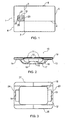
- a hybrid contactless integrated circuit card 1 is provided with a module 10.
- the external dimensions of the card correspond to the "credit card" format defined in the ISO 7810 standard.
- the card comprises two small sides 5 and 6 perpendicular to two large sides 7 and 8.
- the module 10 comprises two small edges 23 and 24 and two large edges 25 and 27.
- the axes of the card most solicited that is to say where the most important constraints are represented by the dashed lines 3 and 4.
- the lines 3 and 4 located along the internal edges 23 and 25 of the module are respectively parallel to the sides 6 and 8 of the map.
- the break zones of the card are located on these lines 3 and 4 at the point of the continuous line along the inner edges of the module.
- the module is located on the card in a portion delimited by a first side 6 of the card, a second side 8 of the card perpendicular to the first side 6, the line 3 and the second line 4.
- the device comprises an electronic module 10 consisting of an electrically nonconductive support 19 bearing on its first face the range of the flush contacts 12 adapted to connect to the contacts of the reading head of the reading device, and on the other side, contacts 13 and 14 adapted to be connected to the antenna of the card.
- An integrated circuit 15 is then connected both to the range of flush contacts 12 by means of welded gold wires 16 passing through the support by holes 11 provided for this purpose and to the contacts 13 and 14 adapted to be The integrated circuit 15 and the wires 16 and 17 are then protected and sealed by a resin 18 cast on top.
- the integrated circuit and the wires are thus encapsulated and only a portion of the contacts 13 and 14 intended to come to connect to the studs of the antenna is apparent as illustrated on FIG. figure 3 .
- the contacts 13 and 14 of the module 10 are situated on either side of the resin 18 and are respectively parallel to the small edges 23 and 24 of the module 10.
- Such a module is called a double-sided integrated circuit module since it comprises contacts on both sides unlike a single-sided integrated circuit module composed only of the range of flush contacts used in the realization of contact IC cards.
- the module is rigid so that it does not flex when the card is subjected to bending or twisting stresses. The connections between the integrated circuit 15 and the contacts 12, 13 and 14 are thus protected from any breakage.
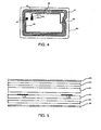
- an antenna 41 is formed on a support layer 40.
- the antenna 41 is formed of a plurality of turns of an electrically conductive material.
- the turns of substantially rectangular shape comprise several straight portions so as to follow the edges of the card.
- the antenna turns intersect at an insulating bridge 48.
- the turns are terminated by two ends 45 and 46 forming two straight antenna portions respectively extended by two connection pads 43 and 44 intended to be electrically connected to both of them. contacts 13 and 14 of the module. Both ends 45 and 46 of the antenna turns are called respectively inner ends and outer end.
- the turns and the connection pads of the antenna are made by screen-printing, flexographic, rotogravure, offset or inkjet printing from conductive epoxy ink filled with conductive particles such as, for example, silver or gold or from a conductive polymer.
- the backing layer 40 is preferably of a material that does not flow (i.e., does not deform under the effect of temperature) such as paper or synthetic paper (teslin type).
- the inner end 45 of the antenna turns is located on the support so as not to cut the line 3.
- the portion of turn 49 which extends the end 45 intersects the line 3 being as far as possible from the edge internal 23 of the module.
- This configuration removes as far as possible the end 45 of the rupture zone.
- the intersection of the turn portion 49 and the line 3 must therefore be located closer to the edge of the map taking into account the location of the other antenna turns.
- the internal connection pad 43 located closest to the center of the card is the most mechanically stressed when the card is subjected to bending tests around the transverse axis of symmetry of the card.
- the external connection pad 44 located near the edge 6 of the card suffers little mechanical stress.
- the two connection pads 43 and 44 are manufactured by printing at least two layers of ink on the antenna support 40.
- the ink layers constituting the external connection pad 44 are superposed on each other. to others and all have the same shape and dimensions.
- the dimensions of the stud 44 are such that its inner surface substantially encompasses the surface of the contact 14 of the module 10. More specifically, the surface of the stud 44 is at least twice the contact surface 14 of the module 10.
- the layers of ink constitutive of the pad 43 designated by layer 43-1 and 43-2 are superimposed on each other and they do not all have the same dimensions.
- the surface of the first ink layer 43-1 of the pad 43 is larger than the surface of the successive ink layers.
- the second layer and the subsequent layers of the first layer 43-1 constituting said pad 43 have the same area as the surface of the constituent layers of the connection pad 44.
- the first ink layer 43-1 of the connection pad 43 is perforated .
- the ink layer 43-1 is made in the form of a mesh whose meshes have spaces 47 where there is no ink. These spaces can be of different forms without this outside the scope of the invention.
- This configuration of the first layer makes it possible to further hook the second layer to the support by bonding a portion of the ink of the second layer directly on the antenna support through the spaces 47 of the first layer so as to avoid that the ink layers constituting the connection pad delaminate.
- the area of the second ink layer 43-2 is smaller than that of the ink layer 43-1 and is equal to the ink layer surfaces of the pad 44. Once all the layers of ink are superposed, the the ink thickness of the antenna pads is between 50 and 80 ⁇ m.
- the card according to the invention comprises a plurality of layers illustrated in section on the figure 5 . Since the figure is not to scale, only the two connection pads 43 and 44 are shown.
- PVC polyvinyl chloride
- PET polyesters
- cover layer 64 On the other side of the antenna support layer 40, are arranged in this order a PET layer 72 and a cover layer 64.
- the lamination step consists of stacking all the layers 40, 61, 63, 65, 62 and 64 and of subjecting it to a heat treatment at a temperature of the order of 150 ° C. under a pressure of the order of 20 Bars. Under the effect of pressure and temperature, the PVC layer 61 softens and encloses the antenna turns and the antenna pads 43 and 44.
- the two layers of PET stiffen the assembly and in particular the layer PET 62 not pierced the cavity in which is housed the module. This configuration of layers constituting the card has the advantage of conferring both resistance and flexibility to the card so that the card does not break during the bending and / or torsion tests.
- the next step is to mill a cavity for receiving the module 10 and stick the module in the cavity.
- This configuration of the end of the antenna turns makes it possible to move the antenna away from the rupture zone located along the edge 23 of the module.
- the end 45 is in the extension of the portion of the internal connection pad 43 located inside the module. In this way, the end 45 of the antenna turns is not likely to be cut off when the card undergoes mechanical bending stresses.
- the stud 44 projects beyond the module on the side of its small external edge 24.
- the surface of the first ink layer 43-1 projects beyond the module on the side of its inner edge 23 and its large external edge 27.
Landscapes
- Engineering & Computer Science (AREA)
- Microelectronics & Electronic Packaging (AREA)
- Computer Hardware Design (AREA)
- Physics & Mathematics (AREA)
- General Physics & Mathematics (AREA)
- Theoretical Computer Science (AREA)
- Computer Networks & Wireless Communication (AREA)
- Credit Cards Or The Like (AREA)
Description
- La présente invention concerne les dispositifs d'identification radiofréquence (RFID) sans contact et concerne en particulier une carte à circuit intégré hybride contact - sans contact à tenue renforcée du module de circuit intégré et son procédé de fabrication.
- Un dispositif RFID sans contact est un dispositif constitué d'une antenne et d'un circuit intégré connecté aux bornes de l'antenne. Le circuit intégré n'est généralement pas alimenté et reçoit son énergie par couplage électromagnétique entre l'antenne du lecteur et l'antenne du dispositif RFID, des informations sont échangées entre le dispositif RFID et le lecteur et en particulier les informations stockées dans le circuit intégré qui ont trait à l'identification du possesseur de l'objet sur lequel se trouve le dispositif RFID et son autorisation à pénétrer dans une zone à accès contrôlé.
- Une carte à circuit intégré hybride contact - sans contact est un dispositif RFID sans contact à la différence que l'échange des données avec le lecteur peut se faire également par contact sur des plages affleurantes et conductrices de la carte connectées au circuit intégré. Le circuit intégré est donc encapsulé dans un module dont la face externe comporte les plages de contacts affleurantes. Le circuit intégré est également connecté à la face interne du module destinée à venir se connecter à l'antenne de la carte. Ainsi, le circuit intégré est connecté aux deux faces d'un module double face de façon à former, une fois encapsulé, un module de circuit intégré double face ou module électronique double face. De ce fait, la tenue du module électronique et donc du circuit intégré sur la carte, est fragilisée par rapport à une carte à circuit intégré sans contact où le circuit intégré est le plus souvent noyé dans le corps de carte. Donc le problème majeur des cartes hybrides contact-sans contact est leur fragilité. En effet, le module est un élément rigide qui ne fléchit pas. Par conséquent, les contraintes sont concentrées autour du module en particulier le long de ses bords internes situés le plus près des axes de symétries de la carte donc du centre de la carte. Généralement, le procédé de fabrication des cartes à circuit intégré hybrides contact - sans contact comprend les étapes suivantes :
- une étape de fabrication de l'antenne sur un support,
- une étape de lamination des corps de carte sur le support de l'antenne consistant à souder de chaque côté du support une ou plusieurs feuilles en matière plastique, constituant les corps de carte, par pressage à chaud,
- une étape de fraisage des cavités consistant à percer, dans un des corps de carte, une cavité permettant de loger le module constitué par le circuit intégré et le circuit double face, la cavité comprenant une portion interne plus petite, recevant le circuit intégré et une portion externe plus grande recevant le module double face, le fraisage permettant de dégager les plots de connexion de l'antenne, et
- une étape d'insertion du module consistant à utiliser une colle permettant de fixer le module et une colle conductrice permettant de connecter le module aux plots de connexion, et à le positionner dans la cavité prévue à cet effet.
- Les cartes à circuit intégré hybrides contact - sans contact sont soumises à des essais de flexion et torsion selon des critères définis dans la norme en vigueur. Un premier type de carte à circuit intégré hybride contact - sans contact est une carte monobloc dans laquelle le support d'antenne en matière plastique, est inséré entre deux couches en matière plastique constituant les corps de carte supérieur et inférieur et thermosoudés par lamination sous pression à chaud. Le module est connecté à l'antenne par une colle conductrice ou équivalent qui permet d'établir le contact ohmique.
- Ce type de carte possède une grande rigidité d'ensemble. Par conséquent, lorsque ce type de carte est soumis à des contraintes mécaniques de flexion ou/et de torsion, les contraintes ne marquent pas la carte mais la carte casse le long des axes où les contraintes se manifestent le plus c'est-à-dire, le long du module.
- Un autre type de carte est muni d'un support d'antenne en papier résistant à la cassure. Ce type de carte présente l'inconvénient de fournir une tenue fragile du module électronique sur la carte. En effet, un support d'antenne en matériau fibreux tel que du papier offre l'avantage de garder "en mémoire" les pliures de la carte, mais confère à la carte un manque de cohésion interne favorisant après de multiples pliures la délamination du papier sous les joints de colle tenant le module sur la carte et donc à la verticale de la partie la moins épaisse du corps de carte, provoquant par conséquent la déconnexion du module électronique et de l'antenne. En général, le premier contact du module qui se déconnecte de l'antenne est celui qui se situe le plus proche du centre de la carte. Le document
WO 02/093472 - C'est pourquoi le but de l'invention est de fournir une carte à circuit intégré hybride contact-sans contact qui remédie à ces inconvénients c'est-à-dire capable de résister à des essais de flexion sans que le corps de carte ne casse ou que la connexion entre le module et l'antenne ou l'antenne ne soit rompue.
- L'objet de l'invention est donc une carte à puce hybride, contact-sans contact, comprenant un corps de carte constitué d'une pluralité de couches dont une des couches, dite couche de support supporte une antenne imprimée constituée d'au moins une spire et supporte un module de circuit intégré connecté à l'antenne par deux plots de connexion interne et externe situés respectivement dans le prolongement des extrémités interne et externe des spires d'antenne, le module étant situé sur la carte dans une portion délimitée par un premier côté de la carte, un second côté de la carte perpendiculaire au premier côté, une première ligne parallèle au premier côté de la carte et une seconde ligne parallèle au second côté de la carte. L'extrémité interne des spires d'antenne reliée au plot interne est située entièrement dans la portion de sorte que lorsque la carte est soumise à des contraintes de flexion ou/et torsion, la connexion entre le module et l'antenne n'est pas rompue. De plus, les plots de connexion sont réalisés par impression d'au moins deux couches d'une encre conductrice superposées l'une à l'autre sur le support, la première couche d'encre comprenant des espaces non recouverts d'encre.
- Les buts, objets et caractéristiques de l'invention apparaîtront plus clairement à la lecture de la description qui suit faite en référence aux dessins dans lesquels :
- La
figure 1 est une vue de dessus d'une carte à circuit intégré hybride contact-sans contact, - La
figure 2 représente une coupe d'un module électronique double face selon l'état de la technique, - La
figure 3 représente le module électronique double face selon l'état de la technique vu du côté du circuit intégré, - La
figure 4 est une vue de dessus du support d'antenne de la carte à circuit intégré hybride contact-sans contact selon l'invention, - La
figure 5 est une coupe des différentes couches constitutives de la carte selon l'invention, - La
figure 6 représente une coupe de la carte selon l'invention muni de son module, - La
figure 7 représente une vue de dessus en transparence du module et des plots de connexion de l'antenne selon l'invention. - De façon générale dans la suite de la description, il est désigné par côté ou bord « interne » les bords et les côtés d'un élément situés géométriquement plus près du centre de la carte que les bords ou les côtés opposés du même élément désigné par « externe ».
- Selon l'illustration de la
figure 1 une carte à circuit intégré hybride contact sans contact 1 est munie d'un module 10. Les dimensions extérieures de la carte correspondent au format « carte de crédit » définies dans la norme ISO 7810. La carte comprend deux petits côtés 5 et 6 perpendiculaires à deux grands côtés 7 et 8. Le module 10 comprend deux petits bords 23 et 24 et deux grands bords 25 et 27. Lors d'essais mécaniques et en particulier lors d'essais en flexion de la carte, les axes de la carte les plus sollicités c'est à dire où les contraintes sont les plus importantes sont représentés par les lignes en pointillés 3 et 4. Les lignes 3 et 4 situées le long des bords internes 23 et 25 du module sont respectivement parallèles aux côtés 6 et 8 de la carte. Les zones de rupture de la carte se situent sur ces lignes 3 et 4 à l'endroit du trait en continu le long des bords internes du module. Le module est situé sur la carte dans une portion délimitée par un premier côté 6 de la carte, un second côté 8 de la carte perpendiculaire au premier côté 6, la ligne 3 et la seconde ligne 4. - Selon la
figure 2 , le dispositif selon l'invention comprend un module électronique 10 constitué d'un support électriquement non conducteur 19 portant sur sa première face la plage des contacts affleurants 12 adaptés pour se connecter aux contacts de la tête de lecture du dispositif de lecture, et sur l'autre face, des contacts 13 et 14 adaptés pour être connectés à l'antenne de la carte. Un circuit intégré 15 est ensuite connectée à la fois à la plage de contacts affleurants 12 à l'aide de fils d'or soudés 16 traversant le support par des trous 11 prévus à cet effet et aux contacts 13 et 14 adaptés pour être connectés à l'antenne également par des fils d'or soudés 17. Le circuit intégré 15 et les fils 16 et 17 sont ensuite protégés et scellés par une résine 18 coulée par dessus. Lorsque la résine est durcie, le circuit intégré et les fils sont ainsi encapsulés et seule une partie des contacts 13 et 14 destinés à venir se connecter aux plots de l'antenne est apparente telle qu'illustrée sur lafigure 3 . Les contacts 13 et 14 du module 10 sont situés de part et d'autre de la résine 18 et sont parallèles respectivement aux petits bords 23 et 24 du module 10. Un tel module est appelé module de circuit intégré double face puisqu'il comprend des contacts sur ses deux faces contrairement à un module de circuit intégré simple face composé uniquement de la plage de contacts affleurants utilisé dans la réalisation des cartes à circuit intégré à contact. Le module est rigide de sorte qu'il ne fléchit pas lorsque la carte est soumise à des contraintes de flexion ou de torsion. Les connexions entre le circuit intégré 15 et les contacts 12, 13 et 14 sont ainsi protégés de toute cassure. - Selon la
figure 4 , une antenne 41 est réalisée sur une couche de support 40. L'antenne 41 est formée d'une pluralité de spires d'un matériau électriquement conducteur. Les spires de forme sensiblement rectangulaires comportent plusieurs portions droites de façon à longer les bords de la carte. Les spires d'antenne se croisent au niveau d'un pont isolant 48. Les spires se terminent par deux extrémités 45 et 46 formant deux portions droites d'antenne prolongées respectivement par deux plots de connexion 43 et 44 destinés à être connectés électriquement aux deux contacts 13 et 14 du module. Les deux extrémités 45 et 46 des spires d'antenne sont appelés respectivement extrémités interne et extrémité externe. Les spires et les plots de connexion de l'antenne sont réalisés par impression de type sérigraphie, flexographie, héliogravure, offset ou jet d'encre à partir d'encre conductrice de type encre époxy chargée de particules conductrices telles que par exemple d'argent ou d'or ou à partir d'un polymère conducteur. La couche de support 40 est de préférence dans un matériau qui ne flue pas (c'est à dire qui ne se déforme pas sous l'effet de la température) tel que du papier ou du papier synthétique (type teslin). - L'extrémité interne 45 des spires d'antennes est située sur le support de façon à ne pas couper la ligne 3. Ainsi, la portion de spire 49 qui prolonge l'extrémité 45 coupe la ligne 3 en étant le plus éloignée possible du bord interne 23 du module. Cette configuration éloigne le plus possible l'extrémité 45 de la zone de rupture. L'intersection de la portion de spire 49 et de la ligne 3 doit donc se situer au plus près du bord de la carte en tenant compte de l'emplacement des autres spires d'antenne. Le plot de connexion interne 43 situé le plus près du centre de la carte est le plus sollicité mécaniquement lorsque la carte est soumise à des essais en flexion autour de l'axe de symétrie transversale de la carte. Le plot de connexion externe 44 situé près du bord 6 de la carte subit peu de contraintes mécaniques. Selon l'invention, les deux plots de connexion 43 et 44 sont fabriqués par impression d'au moins deux couches d'encre sur le support d'antenne 40. Les couches d'encre constitutives du plot de connexion externe 44 se superposent les unes aux autres et ont toutes la même forme et les mêmes dimensions. Les dimensions du plot 44 sont telles que sa surface interne englobe largement la surface du contact 14 du module 10. Plus précisément, la surface du plot 44 est au moins égale à deux fois la surface du contact 14 du module 10. Les couches d'encre constitutives du plot 43 désignées par couche 43-1 et 43-2 se superposent les unes aux autres et elles n'ont pas toutes les mêmes dimensions. La surface de la première couche d'encre 43-1 du plot 43 est plus grande que la surface des couches d'encre successives. La seconde couche et les couches suivantes de la première couche 43-1 constitutive dudit plot 43 ont la même superficie que la surface des couches constitutives du plot de connexion 44. La première couche d'encre 43-1 du plot de connexion 43 est ajourée. Selon le mode de réalisation préféré de l'invention, la couche d'encre 43-1 est réalisée sous forme d'un maillage dont les mailles présentent des espaces 47 où il n'y a pas d'encre. Ces espaces peuvent être de différentes formes sans que cela sorte du cadre de l'invention. Cette configuration de la première couche permet d'accrocher davantage la seconde couche au support par collage d'une partie de l'encre de la seconde couche directement sur le support d'antenne à travers les espaces 47 de la première couche de façon à éviter que les couches d'encre constitutives du plot de connexion se délaminent. La superficie de la seconde couche d'encre 43-2 est inférieure à celle de la couche d'encre 43-1 et est égale aux surfaces des couches d'encre du plot 44. Une fois toutes les couches d'encre superposées, l'épaisseur d'encre des plots d'antenne est comprise entre 50 et 80 µm.
- La carte selon l'invention comprend une pluralité de couches illustrée en coupe sur la
figure 5 . La figure n'étant pas à l'échelle, seuls les deux plots de connexion 43 et 44 sont représentés. Sur la couche de support d'antenne 40 et plus précisément sur la face de la couche 40 où est réalisée l'antenne, sont disposées dans cet ordre une couche de polychlorure de vinyle (PVC) 61, une couche de polyesters (PET) 63 et une couche de couverture 65. Sur l'autre face de la couche de support d'antenne 40, sont disposées dans cet ordre une couche de PET 72 et une couche de couverture 64. - L'étape de lamination consiste à empiler l'ensemble des couches 40, 61, 63, 65, 62 et 64 et à lui faire subir un traitement thermique à une température de l'ordre de 150°C sous une pression de l'ordre de 20 Bars. Sous l'effet de la pression et de la température la couche de PVC 61 se ramollit et vient englober les spires d'antennes et les plots d'antenne 43 et 44. Les deux couches de PET rigidifie l'ensemble et en particulier la couche de PET 62 non percée de la cavité dans laquelle vient se loger le module. Cette configuration de couches constitutives de la carte présente l'avantage de conférer à la fois de la résistance et de la souplesse à la carte de façon à ce que la carte ne casse plus pendant les essais de flexion et/ou de torsion.
- L'étape suivante consiste à fraiser une cavité destinée à recevoir le module 10 et à coller le module dans la cavité.
- Par transparence sur la
figure 7 , on peut voir le module 10 lorsqu'il est dans la position connectée aux plots d'antenne. Les plots 43 et 44 se superposent aux contacts 13 et 14 du module 10. Les extrémités 45 et 46 des spires d'antenne sont parallèles aux petits côtés 23 et 24 du module et perpendiculaires aux grands côtés 25 et 27 du module. Par conséquent, les extrémités 45 et 46 des spires d'antenne ne coupent pas la zone de rupture de la carte c'est-à-dire la zone où les contraintes de flexion sont maximum. Si on prolonge l'extrémité 45 des spires d'antenne dans leur axe, (selon la figure et le mode de réalisation décrit cet axe est une ligne droite), elle traverserait la surface délimitée par le module. L'axe de l'extrémité 45 et le plot de connexion 43 sont configurés de telle façon qu'ils croisent le module 10 en coupant son grand bord externe 27. - Cette configuration de l'extrémité des spires d'antenne permet d'éloigner l'antenne de la zone de rupture située le long du bord 23 du module. De plus, l'extrémité 45 se situe dans le prolongement de la partie du plot de connexion interne 43 située à l'intérieur du module. De cette façon, l'extrémité 45 des spires d'antenne ne risque pas d'être coupée lorsque la carte subit des contraintes mécaniques de flexion.
- Le plot 44 déborde du module du côté de son petit bord externe 24. La surface de la première couche d'encre 43-1 déborde du module du côté de son bord interne 23 et de son grand bord externe 27.
Claims (8)
- Carte à puce (1) hybride, contact - sans contact, comprenant un corps de carte constitué d'une pluralité de couches dont une des couches, dite couche de support (40) supporte une antenne imprimée (41) constituée d'au moins une spire et supporte un module de circuit intégré (10) connecté à ladite antenne par deux plots de connexion interne et externe (43, 44) situés respectivement dans le prolongement des extrémités interne et externe (45, 46) des spires d'antenne, ledit module étant situé sur la carte dans une portion délimitée par un premier côté (6) de la carte, un second côté (8) de la carte perpendiculaire audit premier côté, une première ligne (3) parallèle audit premier côté (6) de la carte et une seconde ligne (4) parallèle audit second côté de la carte,
ladite extrémité interne (45) des spires d'antenne reliée audit plot interne (43) est située entièrement dans ladite portion de sorte que lorsque la carte est soumise à des contraintes de flexion ou/et torsion la connexion entre le module et l'antenne n'est pas rompue et
caractérisée en ce que lesdits plots de connexion (43, 44) sont réalisés par impression d'au moins deux couches d'une encre conductrice superposées l'une à l'autre sur ledit support (40), la première couche d'encre (43-1) comprenant des espaces (47) non recouverts d'encre. - Carte selon la revendication 1, dans laquelle le prolongement (49) de ladite extrémité (45) croise ladite ligne (3), ladite extrémité (45) croise ledit axe (3) et leur intersection se situe le plus éloignée possible sur la carte dudit bord interne (23) dudit module (10).
- Carte selon la revendication 1 ou 2, dans laquelle ladite extrémité (45) se situe dans le prolongement de la partie dudit plot de connexion interne (43) située à l'intérieur du module.
- Carte selon l'une des revendications 1, 2 ou 3, dans laquelle la seconde couche et les couches suivantes de la première couche (43-1) constitutive dudit plot (43) ont la même surface que la surface des couches constitutives dudit plot de connexion (44).
- Carte selon l'une des revendications précédentes, dans laquelle l'épaisseur desdits plots de connexion (43, 44) est comprise entre 50 µm et 80 µm.
- Carte selon la revendication précédente, dans laquelle ladite antenne (41) et ledit module (10) sont noyés dans le polychlorure de vinyle (PVC) (61) de la couche du corps de carte située sur la première face de ladite couche de support (40), la première face étant celle sur laquelle ladite antenne est imprimée.
- Carte selon la revendication 6, dans laquelle la seconde face de la couche de support (40) est recouverte d'une couche de polyesters (PET) (62).
- Carte selon l'une des revendications précédentes dans laquelle ladite couche de PVC (61) est recouverte d'une couche de PET (63).
Applications Claiming Priority (2)
| Application Number | Priority Date | Filing Date | Title |
|---|---|---|---|
| FR1102195A FR2977958A1 (fr) | 2011-07-12 | 2011-07-12 | Carte a circuit integre hybride contact-sans contact a tenue renforcee du module electronique |
| PCT/FR2012/000287 WO2013007897A2 (fr) | 2011-07-12 | 2012-07-12 | Carte à circuit intégré hybride contact - sans contact a tenue renforcée du module électronique |
Publications (2)
| Publication Number | Publication Date |
|---|---|
| EP2732406A2 EP2732406A2 (fr) | 2014-05-21 |
| EP2732406B1 true EP2732406B1 (fr) | 2016-01-13 |
Family
ID=46832442
Family Applications (1)
| Application Number | Title | Priority Date | Filing Date |
|---|---|---|---|
| EP12758516.4A Not-in-force EP2732406B1 (fr) | 2011-07-12 | 2012-07-12 | Carte à circuit intégré hybride contact - sans contact a tenue renforcée du module électronique |
Country Status (11)
| Country | Link |
|---|---|
| US (1) | US20130026238A1 (fr) |
| EP (1) | EP2732406B1 (fr) |
| JP (1) | JP2014521164A (fr) |
| KR (1) | KR20140053116A (fr) |
| CN (1) | CN103765447B (fr) |
| BR (1) | BR112014000667A2 (fr) |
| CA (1) | CA2841742C (fr) |
| FR (1) | FR2977958A1 (fr) |
| MX (1) | MX2014000449A (fr) |
| TW (1) | TWI608423B (fr) |
| WO (1) | WO2013007897A2 (fr) |
Families Citing this family (10)
| Publication number | Priority date | Publication date | Assignee | Title |
|---|---|---|---|---|
| FR2996944B1 (fr) * | 2012-10-15 | 2018-05-04 | Smart Packaging Solutions Sps | Module electronique simplifie pour carte a puce a double interface de communication |
| FR3002108A1 (fr) * | 2013-02-14 | 2014-08-15 | Ask Sa | Procede de fabrication d'une antenne pour dispositif radiofrequence sur support mince et dispositif comprenant une antenne ainsi obtenue |
| US9536188B2 (en) | 2014-04-01 | 2017-01-03 | Nxp B.V. | Dual-interface IC card components and method for manufacturing the dual-interface IC card components |
| US9424507B2 (en) | 2014-04-01 | 2016-08-23 | Nxp B.V. | Dual interface IC card components and method for manufacturing the dual-interface IC card components |
| GB2525869A (en) * | 2014-05-06 | 2015-11-11 | Johnson Electric Sa | Smart card module |
| US10984304B2 (en) | 2017-02-02 | 2021-04-20 | Jonny B. Vu | Methods for placing an EMV chip onto a metal card |
| USD877739S1 (en) * | 2017-09-15 | 2020-03-10 | uQontrol, Inc. | Smartcard with Q-shaped contact pad |
| FR3073307B1 (fr) * | 2017-11-08 | 2021-05-28 | Oberthur Technologies | Dispositif de securite tel qu'une carte a puce |
| USD956760S1 (en) * | 2018-07-30 | 2022-07-05 | Lion Credit Card Inc. | Multi EMV chip card |
| JP7424073B2 (ja) * | 2020-01-28 | 2024-01-30 | Toppanホールディングス株式会社 | デュアルicカード |
Family Cites Families (20)
| Publication number | Priority date | Publication date | Assignee | Title |
|---|---|---|---|---|
| JPH02125796A (ja) * | 1988-11-04 | 1990-05-14 | Nec Corp | Icカード |
| JPH0320183U (fr) * | 1989-07-05 | 1991-02-27 | ||
| DE19541072A1 (de) * | 1995-11-03 | 1997-05-07 | Siemens Ag | Chipmodul |
| FR2780848A1 (fr) * | 1998-07-06 | 2000-01-07 | Solaic Sa | Antenne a bornes de connexion ajourees pour carte a circuit integre, et carte a circuit integre comprenant une telle antenne |
| JP3717701B2 (ja) * | 1999-04-19 | 2005-11-16 | 凸版印刷株式会社 | ハイブリッド型icカードの製造方法 |
| FR2801707B1 (fr) * | 1999-11-29 | 2002-02-15 | A S K | Procede de fabrication d'une carte a puce hybride contact- sans contact avec un support d'antenne en materiau fibreux |
| JP2002140673A (ja) * | 2000-11-01 | 2002-05-17 | Toppan Printing Co Ltd | 複合icカード |
| FR2824939B1 (fr) * | 2001-05-16 | 2003-10-10 | A S K | Procede de fabrication d'une carte a puce sans contact a l'aide de papier transfert et carte a puce obtenue a partir de ce procede |
| FR2829857B1 (fr) * | 2001-09-14 | 2004-09-17 | A S K | Carte a puce sans contact ou hybride contact-sans contact a tenue renforcee du module electronique |
| GB2380068B (en) * | 2001-09-15 | 2005-08-03 | Jaybee Graphics | Low Conductive Ink Composition |
| JP2004185208A (ja) * | 2002-12-02 | 2004-07-02 | Sony Corp | Icカード |
| JP2004280503A (ja) * | 2003-03-17 | 2004-10-07 | Toppan Printing Co Ltd | コンビネーションicカード |
| FR2853115B1 (fr) * | 2003-03-28 | 2005-05-06 | A S K | Procede de fabrication d'antenne de carte a puce sur un support thermoplastique et carte a puce obtenue par ledit procede |
| JP4090950B2 (ja) * | 2003-06-26 | 2008-05-28 | 大日本印刷株式会社 | 複合icカード用icモジュール |
| FR2880160B1 (fr) * | 2004-12-28 | 2007-03-30 | K Sa As | Module electronique double face pour carte a puce hybride |
| JP2008090693A (ja) * | 2006-10-04 | 2008-04-17 | Sharp Corp | Icカード及びその製造方法 |
| DE102006054449A1 (de) * | 2006-11-16 | 2008-05-21 | Smartrac Ip B.V. | Transpondereinheit |
| TW200912763A (en) * | 2007-09-14 | 2009-03-16 | Taiwan Name Plate Co Ltd | Card structure with printed RFID |
| CN101971194A (zh) * | 2007-12-19 | 2011-02-09 | 谢玉莲 | 非接触式和双界面嵌体及其生产方法 |
| JP2010033137A (ja) * | 2008-07-25 | 2010-02-12 | Toppan Printing Co Ltd | デュアルicカード、およびその製造方法 |
-
2011
- 2011-07-12 FR FR1102195A patent/FR2977958A1/fr active Pending
-
2012
- 2012-07-12 CA CA2841742A patent/CA2841742C/fr not_active Expired - Fee Related
- 2012-07-12 KR KR1020147001585A patent/KR20140053116A/ko not_active Withdrawn
- 2012-07-12 US US13/547,827 patent/US20130026238A1/en not_active Abandoned
- 2012-07-12 BR BR112014000667A patent/BR112014000667A2/pt not_active Application Discontinuation
- 2012-07-12 CN CN201280042198.9A patent/CN103765447B/zh not_active Expired - Fee Related
- 2012-07-12 JP JP2014519598A patent/JP2014521164A/ja active Pending
- 2012-07-12 TW TW101125231A patent/TWI608423B/zh not_active IP Right Cessation
- 2012-07-12 WO PCT/FR2012/000287 patent/WO2013007897A2/fr not_active Ceased
- 2012-07-12 MX MX2014000449A patent/MX2014000449A/es active IP Right Grant
- 2012-07-12 EP EP12758516.4A patent/EP2732406B1/fr not_active Not-in-force
Also Published As
| Publication number | Publication date |
|---|---|
| US20130026238A1 (en) | 2013-01-31 |
| TWI608423B (zh) | 2017-12-11 |
| KR20140053116A (ko) | 2014-05-07 |
| WO2013007897A3 (fr) | 2013-03-28 |
| MX2014000449A (es) | 2014-04-10 |
| WO2013007897A2 (fr) | 2013-01-17 |
| EP2732406A2 (fr) | 2014-05-21 |
| BR112014000667A2 (pt) | 2017-02-14 |
| CN103765447B (zh) | 2017-02-15 |
| JP2014521164A (ja) | 2014-08-25 |
| FR2977958A1 (fr) | 2013-01-18 |
| CA2841742A1 (fr) | 2013-01-17 |
| TW201319951A (zh) | 2013-05-16 |
| CA2841742C (fr) | 2019-10-22 |
| CN103765447A (zh) | 2014-04-30 |
Similar Documents
| Publication | Publication Date | Title |
|---|---|---|
| EP2732406B1 (fr) | Carte à circuit intégré hybride contact - sans contact a tenue renforcée du module électronique | |
| EP2143046B1 (fr) | Carte à puce, procédé et système pour la fabrication d'une carte à puce. | |
| ES3061919T3 (en) | Chip card and method for fabricating a chip card | |
| EP2203875B1 (fr) | Support de dispositif d'identification radiofréquence pour passeport et son procédé de fabrication | |
| WO2012007659A1 (fr) | Dispositif d'identification radio fréquence en polycarbonate et son procédé de fabrication | |
| FR2880160A1 (fr) | Module electronique double face pour carte a puce hybride | |
| FR2948796A1 (fr) | Support de dispositif d'identification radiofrequence pour carte hybride et son procede de fabrication | |
| FR2900484A1 (fr) | Support de dispositif d'identification radiofrequence et son procede de fabrication | |
| EP3005244A1 (fr) | Procede de fabrication d'un dispositif electronique anti-fissuration | |
| FR2900485A1 (fr) | Support de dispositif d'identification radiofrequence et son procede de fabrication | |
| EP3182507A1 (fr) | Module antenne simple face avec composant cms | |
| WO2017191414A1 (fr) | Procédé de fabrication de cartes à puce et carte à puce obtenue par ce procédé | |
| EP2021985B1 (fr) | Support de dispositif d'identification radiofrequence et son procede de fabrication | |
| JP2007115090A (ja) | 非接触icインレットとそれを備えた非接触ic付き情報記録媒体及び非接触icインレットの製造方法 | |
| EP2631849A1 (fr) | Procédé de fabrication d'un dispositif comprenant un module doté d'un circuit électrique et/ou électronique | |
| HK1196685A (en) | Hybrid contact/contactless integrated circuit card, the strength of the electronic module of which is reinforced | |
| HK1196685B (en) | Hybrid contact/contactless integrated circuit card, the strength of the electronic module of which is reinforced |
Legal Events
| Date | Code | Title | Description |
|---|---|---|---|
| PUAI | Public reference made under article 153(3) epc to a published international application that has entered the european phase |
Free format text: ORIGINAL CODE: 0009012 |
|
| 17P | Request for examination filed |
Effective date: 20140210 |
|
| AK | Designated contracting states |
Kind code of ref document: A2 Designated state(s): AL AT BE BG CH CY CZ DE DK EE ES FI FR GB GR HR HU IE IS IT LI LT LU LV MC MK MT NL NO PL PT RO RS SE SI SK SM TR |
|
| DAX | Request for extension of the european patent (deleted) | ||
| GRAP | Despatch of communication of intention to grant a patent |
Free format text: ORIGINAL CODE: EPIDOSNIGR1 |
|
| INTG | Intention to grant announced |
Effective date: 20150716 |
|
| GRAS | Grant fee paid |
Free format text: ORIGINAL CODE: EPIDOSNIGR3 |
|
| GRAA | (expected) grant |
Free format text: ORIGINAL CODE: 0009210 |
|
| AK | Designated contracting states |
Kind code of ref document: B1 Designated state(s): AL AT BE BG CH CY CZ DE DK EE ES FI FR GB GR HR HU IE IS IT LI LT LU LV MC MK MT NL NO PL PT RO RS SE SI SK SM TR |
|
| REG | Reference to a national code |
Ref country code: GB Ref legal event code: FG4D Free format text: NOT ENGLISH |
|
| REG | Reference to a national code |
Ref country code: CH Ref legal event code: EP |
|
| REG | Reference to a national code |
Ref country code: IE Ref legal event code: FG4D Free format text: LANGUAGE OF EP DOCUMENT: FRENCH |
|
| REG | Reference to a national code |
Ref country code: AT Ref legal event code: REF Ref document number: 770963 Country of ref document: AT Kind code of ref document: T Effective date: 20160215 |
|
| REG | Reference to a national code |
Ref country code: DE Ref legal event code: R096 Ref document number: 602012013928 Country of ref document: DE |
|
| REG | Reference to a national code |
Ref country code: LT Ref legal event code: MG4D |
|
| REG | Reference to a national code |
Ref country code: NL Ref legal event code: MP Effective date: 20160113 |
|
| REG | Reference to a national code |
Ref country code: AT Ref legal event code: MK05 Ref document number: 770963 Country of ref document: AT Kind code of ref document: T Effective date: 20160113 |
|
| PG25 | Lapsed in a contracting state [announced via postgrant information from national office to epo] |
Ref country code: NL Free format text: LAPSE BECAUSE OF FAILURE TO SUBMIT A TRANSLATION OF THE DESCRIPTION OR TO PAY THE FEE WITHIN THE PRESCRIBED TIME-LIMIT Effective date: 20160113 |
|
| PG25 | Lapsed in a contracting state [announced via postgrant information from national office to epo] |
Ref country code: NO Free format text: LAPSE BECAUSE OF FAILURE TO SUBMIT A TRANSLATION OF THE DESCRIPTION OR TO PAY THE FEE WITHIN THE PRESCRIBED TIME-LIMIT Effective date: 20160413 Ref country code: HR Free format text: LAPSE BECAUSE OF FAILURE TO SUBMIT A TRANSLATION OF THE DESCRIPTION OR TO PAY THE FEE WITHIN THE PRESCRIBED TIME-LIMIT Effective date: 20160113 Ref country code: FI Free format text: LAPSE BECAUSE OF FAILURE TO SUBMIT A TRANSLATION OF THE DESCRIPTION OR TO PAY THE FEE WITHIN THE PRESCRIBED TIME-LIMIT Effective date: 20160113 Ref country code: ES Free format text: LAPSE BECAUSE OF FAILURE TO SUBMIT A TRANSLATION OF THE DESCRIPTION OR TO PAY THE FEE WITHIN THE PRESCRIBED TIME-LIMIT Effective date: 20160113 Ref country code: IT Free format text: LAPSE BECAUSE OF FAILURE TO SUBMIT A TRANSLATION OF THE DESCRIPTION OR TO PAY THE FEE WITHIN THE PRESCRIBED TIME-LIMIT Effective date: 20160113 Ref country code: GR Free format text: LAPSE BECAUSE OF FAILURE TO SUBMIT A TRANSLATION OF THE DESCRIPTION OR TO PAY THE FEE WITHIN THE PRESCRIBED TIME-LIMIT Effective date: 20160414 |
|
| PG25 | Lapsed in a contracting state [announced via postgrant information from national office to epo] |
Ref country code: IS Free format text: LAPSE BECAUSE OF FAILURE TO SUBMIT A TRANSLATION OF THE DESCRIPTION OR TO PAY THE FEE WITHIN THE PRESCRIBED TIME-LIMIT Effective date: 20160513 Ref country code: SE Free format text: LAPSE BECAUSE OF FAILURE TO SUBMIT A TRANSLATION OF THE DESCRIPTION OR TO PAY THE FEE WITHIN THE PRESCRIBED TIME-LIMIT Effective date: 20160113 Ref country code: LT Free format text: LAPSE BECAUSE OF FAILURE TO SUBMIT A TRANSLATION OF THE DESCRIPTION OR TO PAY THE FEE WITHIN THE PRESCRIBED TIME-LIMIT Effective date: 20160113 Ref country code: AT Free format text: LAPSE BECAUSE OF FAILURE TO SUBMIT A TRANSLATION OF THE DESCRIPTION OR TO PAY THE FEE WITHIN THE PRESCRIBED TIME-LIMIT Effective date: 20160113 Ref country code: PT Free format text: LAPSE BECAUSE OF FAILURE TO SUBMIT A TRANSLATION OF THE DESCRIPTION OR TO PAY THE FEE WITHIN THE PRESCRIBED TIME-LIMIT Effective date: 20160513 Ref country code: RS Free format text: LAPSE BECAUSE OF FAILURE TO SUBMIT A TRANSLATION OF THE DESCRIPTION OR TO PAY THE FEE WITHIN THE PRESCRIBED TIME-LIMIT Effective date: 20160113 Ref country code: LV Free format text: LAPSE BECAUSE OF FAILURE TO SUBMIT A TRANSLATION OF THE DESCRIPTION OR TO PAY THE FEE WITHIN THE PRESCRIBED TIME-LIMIT Effective date: 20160113 Ref country code: PL Free format text: LAPSE BECAUSE OF FAILURE TO SUBMIT A TRANSLATION OF THE DESCRIPTION OR TO PAY THE FEE WITHIN THE PRESCRIBED TIME-LIMIT Effective date: 20160113 |
|
| REG | Reference to a national code |
Ref country code: DE Ref legal event code: R097 Ref document number: 602012013928 Country of ref document: DE |
|
| PG25 | Lapsed in a contracting state [announced via postgrant information from national office to epo] |
Ref country code: EE Free format text: LAPSE BECAUSE OF FAILURE TO SUBMIT A TRANSLATION OF THE DESCRIPTION OR TO PAY THE FEE WITHIN THE PRESCRIBED TIME-LIMIT Effective date: 20160113 Ref country code: DK Free format text: LAPSE BECAUSE OF FAILURE TO SUBMIT A TRANSLATION OF THE DESCRIPTION OR TO PAY THE FEE WITHIN THE PRESCRIBED TIME-LIMIT Effective date: 20160113 |
|
| PLBE | No opposition filed within time limit |
Free format text: ORIGINAL CODE: 0009261 |
|
| STAA | Information on the status of an ep patent application or granted ep patent |
Free format text: STATUS: NO OPPOSITION FILED WITHIN TIME LIMIT |
|
| PG25 | Lapsed in a contracting state [announced via postgrant information from national office to epo] |
Ref country code: SM Free format text: LAPSE BECAUSE OF FAILURE TO SUBMIT A TRANSLATION OF THE DESCRIPTION OR TO PAY THE FEE WITHIN THE PRESCRIBED TIME-LIMIT Effective date: 20160113 Ref country code: CZ Free format text: LAPSE BECAUSE OF FAILURE TO SUBMIT A TRANSLATION OF THE DESCRIPTION OR TO PAY THE FEE WITHIN THE PRESCRIBED TIME-LIMIT Effective date: 20160113 Ref country code: RO Free format text: LAPSE BECAUSE OF FAILURE TO SUBMIT A TRANSLATION OF THE DESCRIPTION OR TO PAY THE FEE WITHIN THE PRESCRIBED TIME-LIMIT Effective date: 20160113 Ref country code: SK Free format text: LAPSE BECAUSE OF FAILURE TO SUBMIT A TRANSLATION OF THE DESCRIPTION OR TO PAY THE FEE WITHIN THE PRESCRIBED TIME-LIMIT Effective date: 20160113 |
|
| 26N | No opposition filed |
Effective date: 20161014 |
|
| PG25 | Lapsed in a contracting state [announced via postgrant information from national office to epo] |
Ref country code: BE Free format text: LAPSE BECAUSE OF NON-PAYMENT OF DUE FEES Effective date: 20160731 |
|
| REG | Reference to a national code |
Ref country code: DE Ref legal event code: R119 Ref document number: 602012013928 Country of ref document: DE |
|
| PG25 | Lapsed in a contracting state [announced via postgrant information from national office to epo] |
Ref country code: BG Free format text: LAPSE BECAUSE OF FAILURE TO SUBMIT A TRANSLATION OF THE DESCRIPTION OR TO PAY THE FEE WITHIN THE PRESCRIBED TIME-LIMIT Effective date: 20160413 Ref country code: SI Free format text: LAPSE BECAUSE OF FAILURE TO SUBMIT A TRANSLATION OF THE DESCRIPTION OR TO PAY THE FEE WITHIN THE PRESCRIBED TIME-LIMIT Effective date: 20160113 |
|
| REG | Reference to a national code |
Ref country code: CH Ref legal event code: PL |
|
| GBPC | Gb: european patent ceased through non-payment of renewal fee |
Effective date: 20160712 |
|
| PG25 | Lapsed in a contracting state [announced via postgrant information from national office to epo] |
Ref country code: MC Free format text: LAPSE BECAUSE OF FAILURE TO SUBMIT A TRANSLATION OF THE DESCRIPTION OR TO PAY THE FEE WITHIN THE PRESCRIBED TIME-LIMIT Effective date: 20160113 |
|
| PG25 | Lapsed in a contracting state [announced via postgrant information from national office to epo] |
Ref country code: CH Free format text: LAPSE BECAUSE OF NON-PAYMENT OF DUE FEES Effective date: 20160731 Ref country code: FR Free format text: LAPSE BECAUSE OF NON-PAYMENT OF DUE FEES Effective date: 20160801 Ref country code: DE Free format text: LAPSE BECAUSE OF NON-PAYMENT OF DUE FEES Effective date: 20170201 Ref country code: LI Free format text: LAPSE BECAUSE OF NON-PAYMENT OF DUE FEES Effective date: 20160731 |
|
| REG | Reference to a national code |
Ref country code: FR Ref legal event code: ST Effective date: 20170331 |
|
| REG | Reference to a national code |
Ref country code: IE Ref legal event code: MM4A |
|
| PG25 | Lapsed in a contracting state [announced via postgrant information from national office to epo] |
Ref country code: GB Free format text: LAPSE BECAUSE OF NON-PAYMENT OF DUE FEES Effective date: 20160712 |
|
| PG25 | Lapsed in a contracting state [announced via postgrant information from national office to epo] |
Ref country code: IE Free format text: LAPSE BECAUSE OF NON-PAYMENT OF DUE FEES Effective date: 20160712 |
|
| PG25 | Lapsed in a contracting state [announced via postgrant information from national office to epo] |
Ref country code: LU Free format text: LAPSE BECAUSE OF NON-PAYMENT OF DUE FEES Effective date: 20160712 |
|
| PG25 | Lapsed in a contracting state [announced via postgrant information from national office to epo] |
Ref country code: CY Free format text: LAPSE BECAUSE OF FAILURE TO SUBMIT A TRANSLATION OF THE DESCRIPTION OR TO PAY THE FEE WITHIN THE PRESCRIBED TIME-LIMIT Effective date: 20160113 Ref country code: HU Free format text: LAPSE BECAUSE OF FAILURE TO SUBMIT A TRANSLATION OF THE DESCRIPTION OR TO PAY THE FEE WITHIN THE PRESCRIBED TIME-LIMIT; INVALID AB INITIO Effective date: 20120712 |
|
| PG25 | Lapsed in a contracting state [announced via postgrant information from national office to epo] |
Ref country code: MT Free format text: LAPSE BECAUSE OF FAILURE TO SUBMIT A TRANSLATION OF THE DESCRIPTION OR TO PAY THE FEE WITHIN THE PRESCRIBED TIME-LIMIT Effective date: 20160113 Ref country code: MK Free format text: LAPSE BECAUSE OF FAILURE TO SUBMIT A TRANSLATION OF THE DESCRIPTION OR TO PAY THE FEE WITHIN THE PRESCRIBED TIME-LIMIT Effective date: 20160113 |
|
| PG25 | Lapsed in a contracting state [announced via postgrant information from national office to epo] |
Ref country code: AL Free format text: LAPSE BECAUSE OF FAILURE TO SUBMIT A TRANSLATION OF THE DESCRIPTION OR TO PAY THE FEE WITHIN THE PRESCRIBED TIME-LIMIT Effective date: 20160113 Ref country code: TR Free format text: LAPSE BECAUSE OF FAILURE TO SUBMIT A TRANSLATION OF THE DESCRIPTION OR TO PAY THE FEE WITHIN THE PRESCRIBED TIME-LIMIT Effective date: 20160113 |