EP2734893B1 - Dispositif d'affichage - Google Patents
Dispositif d'affichage Download PDFInfo
- Publication number
- EP2734893B1 EP2734893B1 EP12815312.9A EP12815312A EP2734893B1 EP 2734893 B1 EP2734893 B1 EP 2734893B1 EP 12815312 A EP12815312 A EP 12815312A EP 2734893 B1 EP2734893 B1 EP 2734893B1
- Authority
- EP
- European Patent Office
- Prior art keywords
- wavelength conversion
- conversion member
- light
- heat transfer
- transfer part
- Prior art date
- Legal status (The legal status is an assumption and is not a legal conclusion. Google has not performed a legal analysis and makes no representation as to the accuracy of the status listed.)
- Active
Links
Images



Classifications
-
- G—PHYSICS
- G02—OPTICS
- G02F—OPTICAL DEVICES OR ARRANGEMENTS FOR THE CONTROL OF LIGHT BY MODIFICATION OF THE OPTICAL PROPERTIES OF THE MEDIA OF THE ELEMENTS INVOLVED THEREIN; NON-LINEAR OPTICS; FREQUENCY-CHANGING OF LIGHT; OPTICAL LOGIC ELEMENTS; OPTICAL ANALOGUE/DIGITAL CONVERTERS
- G02F1/00—Devices or arrangements for the control of the intensity, colour, phase, polarisation or direction of light arriving from an independent light source, e.g. switching, gating or modulating; Non-linear optics
- G02F1/01—Devices or arrangements for the control of the intensity, colour, phase, polarisation or direction of light arriving from an independent light source, e.g. switching, gating or modulating; Non-linear optics for the control of the intensity, phase, polarisation or colour
- G02F1/13—Devices or arrangements for the control of the intensity, colour, phase, polarisation or direction of light arriving from an independent light source, e.g. switching, gating or modulating; Non-linear optics for the control of the intensity, phase, polarisation or colour based on liquid crystals, e.g. single liquid crystal display cells
- G02F1/133—Constructional arrangements; Operation of liquid crystal cells; Circuit arrangements
- G02F1/1333—Constructional arrangements; Manufacturing methods
- G02F1/1335—Structural association of cells with optical devices, e.g. polarisers or reflectors
-
- G—PHYSICS
- G02—OPTICS
- G02B—OPTICAL ELEMENTS, SYSTEMS OR APPARATUS
- G02B6/00—Light guides; Structural details of arrangements comprising light guides and other optical elements, e.g. couplings
- G02B6/0001—Light guides; Structural details of arrangements comprising light guides and other optical elements, e.g. couplings specially adapted for lighting devices or systems
- G02B6/0011—Light guides; Structural details of arrangements comprising light guides and other optical elements, e.g. couplings specially adapted for lighting devices or systems the light guides being planar or of plate-like form
- G02B6/0081—Mechanical or electrical aspects of the light guide and light source in the lighting device peculiar to the adaptation to planar light guides, e.g. concerning packaging
- G02B6/0085—Means for removing heat created by the light source from the package
-
- G—PHYSICS
- G02—OPTICS
- G02F—OPTICAL DEVICES OR ARRANGEMENTS FOR THE CONTROL OF LIGHT BY MODIFICATION OF THE OPTICAL PROPERTIES OF THE MEDIA OF THE ELEMENTS INVOLVED THEREIN; NON-LINEAR OPTICS; FREQUENCY-CHANGING OF LIGHT; OPTICAL LOGIC ELEMENTS; OPTICAL ANALOGUE/DIGITAL CONVERTERS
- G02F1/00—Devices or arrangements for the control of the intensity, colour, phase, polarisation or direction of light arriving from an independent light source, e.g. switching, gating or modulating; Non-linear optics
- G02F1/01—Devices or arrangements for the control of the intensity, colour, phase, polarisation or direction of light arriving from an independent light source, e.g. switching, gating or modulating; Non-linear optics for the control of the intensity, phase, polarisation or colour
- G02F1/13—Devices or arrangements for the control of the intensity, colour, phase, polarisation or direction of light arriving from an independent light source, e.g. switching, gating or modulating; Non-linear optics for the control of the intensity, phase, polarisation or colour based on liquid crystals, e.g. single liquid crystal display cells
- G02F1/133—Constructional arrangements; Operation of liquid crystal cells; Circuit arrangements
- G02F1/1333—Constructional arrangements; Manufacturing methods
- G02F1/1335—Structural association of cells with optical devices, e.g. polarisers or reflectors
- G02F1/1336—Illuminating devices
- G02F1/133621—Illuminating devices providing coloured light
-
- G—PHYSICS
- G02—OPTICS
- G02B—OPTICAL ELEMENTS, SYSTEMS OR APPARATUS
- G02B5/00—Optical elements other than lenses
- G02B5/20—Filters
- G02B5/22—Absorbing filters
- G02B5/23—Photochromic filters
-
- G—PHYSICS
- G02—OPTICS
- G02B—OPTICAL ELEMENTS, SYSTEMS OR APPARATUS
- G02B6/00—Light guides; Structural details of arrangements comprising light guides and other optical elements, e.g. couplings
- G02B6/0001—Light guides; Structural details of arrangements comprising light guides and other optical elements, e.g. couplings specially adapted for lighting devices or systems
- G02B6/0011—Light guides; Structural details of arrangements comprising light guides and other optical elements, e.g. couplings specially adapted for lighting devices or systems the light guides being planar or of plate-like form
- G02B6/0013—Means for improving the coupling-in of light from the light source into the light guide
- G02B6/0023—Means for improving the coupling-in of light from the light source into the light guide provided by one optical element, or plurality thereof, placed between the light guide and the light source, or around the light source
-
- G—PHYSICS
- G02—OPTICS
- G02F—OPTICAL DEVICES OR ARRANGEMENTS FOR THE CONTROL OF LIGHT BY MODIFICATION OF THE OPTICAL PROPERTIES OF THE MEDIA OF THE ELEMENTS INVOLVED THEREIN; NON-LINEAR OPTICS; FREQUENCY-CHANGING OF LIGHT; OPTICAL LOGIC ELEMENTS; OPTICAL ANALOGUE/DIGITAL CONVERTERS
- G02F1/00—Devices or arrangements for the control of the intensity, colour, phase, polarisation or direction of light arriving from an independent light source, e.g. switching, gating or modulating; Non-linear optics
- G02F1/01—Devices or arrangements for the control of the intensity, colour, phase, polarisation or direction of light arriving from an independent light source, e.g. switching, gating or modulating; Non-linear optics for the control of the intensity, phase, polarisation or colour
- G02F1/13—Devices or arrangements for the control of the intensity, colour, phase, polarisation or direction of light arriving from an independent light source, e.g. switching, gating or modulating; Non-linear optics for the control of the intensity, phase, polarisation or colour based on liquid crystals, e.g. single liquid crystal display cells
- G02F1/133—Constructional arrangements; Operation of liquid crystal cells; Circuit arrangements
- G02F1/1333—Constructional arrangements; Manufacturing methods
- G02F1/1335—Structural association of cells with optical devices, e.g. polarisers or reflectors
- G02F1/1336—Illuminating devices
- G02F1/133615—Edge-illuminating devices, i.e. illuminating from the side
-
- G—PHYSICS
- G02—OPTICS
- G02F—OPTICAL DEVICES OR ARRANGEMENTS FOR THE CONTROL OF LIGHT BY MODIFICATION OF THE OPTICAL PROPERTIES OF THE MEDIA OF THE ELEMENTS INVOLVED THEREIN; NON-LINEAR OPTICS; FREQUENCY-CHANGING OF LIGHT; OPTICAL LOGIC ELEMENTS; OPTICAL ANALOGUE/DIGITAL CONVERTERS
- G02F1/00—Devices or arrangements for the control of the intensity, colour, phase, polarisation or direction of light arriving from an independent light source, e.g. switching, gating or modulating; Non-linear optics
- G02F1/01—Devices or arrangements for the control of the intensity, colour, phase, polarisation or direction of light arriving from an independent light source, e.g. switching, gating or modulating; Non-linear optics for the control of the intensity, phase, polarisation or colour
- G02F1/13—Devices or arrangements for the control of the intensity, colour, phase, polarisation or direction of light arriving from an independent light source, e.g. switching, gating or modulating; Non-linear optics for the control of the intensity, phase, polarisation or colour based on liquid crystals, e.g. single liquid crystal display cells
- G02F1/133—Constructional arrangements; Operation of liquid crystal cells; Circuit arrangements
- G02F1/1333—Constructional arrangements; Manufacturing methods
- G02F1/133382—Heating or cooling of liquid crystal cells other than for activation, e.g. circuits or arrangements for temperature control, stabilisation or uniform distribution over the cell
- G02F1/133385—Heating or cooling of liquid crystal cells other than for activation, e.g. circuits or arrangements for temperature control, stabilisation or uniform distribution over the cell with cooling means, e.g. fans
-
- G—PHYSICS
- G02—OPTICS
- G02F—OPTICAL DEVICES OR ARRANGEMENTS FOR THE CONTROL OF LIGHT BY MODIFICATION OF THE OPTICAL PROPERTIES OF THE MEDIA OF THE ELEMENTS INVOLVED THEREIN; NON-LINEAR OPTICS; FREQUENCY-CHANGING OF LIGHT; OPTICAL LOGIC ELEMENTS; OPTICAL ANALOGUE/DIGITAL CONVERTERS
- G02F1/00—Devices or arrangements for the control of the intensity, colour, phase, polarisation or direction of light arriving from an independent light source, e.g. switching, gating or modulating; Non-linear optics
- G02F1/01—Devices or arrangements for the control of the intensity, colour, phase, polarisation or direction of light arriving from an independent light source, e.g. switching, gating or modulating; Non-linear optics for the control of the intensity, phase, polarisation or colour
- G02F1/13—Devices or arrangements for the control of the intensity, colour, phase, polarisation or direction of light arriving from an independent light source, e.g. switching, gating or modulating; Non-linear optics for the control of the intensity, phase, polarisation or colour based on liquid crystals, e.g. single liquid crystal display cells
- G02F1/133—Constructional arrangements; Operation of liquid crystal cells; Circuit arrangements
- G02F1/1333—Constructional arrangements; Manufacturing methods
- G02F1/1335—Structural association of cells with optical devices, e.g. polarisers or reflectors
- G02F1/1336—Illuminating devices
- G02F1/133614—Illuminating devices using photoluminescence, e.g. phosphors illuminated by UV or blue light
Definitions
- Some display devices require a backlight unit to generate light in order to display an image.
- the backlight unit supplies the light to a display panel including liquid crystal.
- the backlight unit includes a light emitting device and units to effectively transfer light output from the light emitting device toward the liquid crystal.
- the heat transfer part transfers the heat, which is dissipated from the light source to the wavelength conversion member, to the heat dissipation part. Further, the display device according to the invention dissipates heat generated from the wavelength conversion member by light output from the light source using the heat transfer part and the heat dissipation part.
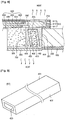
- the light conversion member 400 includes a tube 410, a sealing member 420, a plurality of wavelength conversion particles 430, and a matrix 440.
- the quantum dots can be synthesized through the chemical wet scheme.
- the chemical wet scheme is to grow the particles by immersing the precursor material in the organic solvent. According to the chemical wet scheme, the quantum dots can be synthesized.
- the first inclined surface 402 extends from the incident surface 401 of the wavelength conversion member 400 to the exit surface 404 of the wavelength conversion member 400.
- the first inclined surface 402 is inclined with respect to the incident surface 401 of the wavelength conversion member 400.
- the first inclined surface 402 is inclined with respect to a virtual surface, which is perpendicular to the optical axis OA of the light emitting diode 300.
- the heat transfer part 700 may include a polymer having a high thermal conductivity and transmissivity.
- the material constituting the heat transfer part 700 may include silicon resin, epoxy resin, phenolic resin, urethane resin, or urea resin.
- the first protective layer 640 is provided on the first interconnection layer 620.
- the first protective layer 640 covers the first interconnection layer 620.
- the first protective layer 640 protects the first interconnection layer 620.
- the first protective layer 640 may include an insulator such as polymer.
- the heat transfer part 700 transfers the heat, which is dissipated from the light emitting diode 300 to the wavelength conversion member 400, to the heat dissipation part 800. Further, the display device according to the embodiment dissipates heat generated from the wavelength conversion member 400 by light output from the light source using the heat transfer part 700 and the heat dissipation part 800.
- the display device can prevent the wavelength conversion member 400 from being degraded or denatured due to the heat.
- the display device may prevent a host 440 and/or a wavelength conversion particles 430 from being denatured caused by heat. Therefore, the liquid crystal display according to the embodiment can represent improved reliability and durability.
- the liquid crystal display according to this example can effectively dissipate the heat of the wavelength conversion member 400.
- FIG. 9 is a perspective view showing a wavelength conversion member according to a further example not falling under the scope of the claims and FIG. 10 is a sectional view showing a light emitting diode, a flexible printed circuit board, a wavelength conversion member, and a light guide plate according to this further example.
- the wavelength conversion member according to this further example will be described by making reference to the above description of the liquid crystal display.
- the wavelength conversion member 400 may have the trapezoidal sectional shape.
- an obtuse angle is formed between the top surface 405 and the incident surface 401 of the wavelength conversion member 400, and an acute angle is formed between the bottom surface 406 and the incident surface 401 of the wavelength conversion member 400.
- the distance D between the incident surface 401 of the wavelength conversion member 400 and the exit surface of the light emitting diode 300 is gradually increased in the upward direction. That is, the lower portion of the wavelength conversion member 400 is closer to the light emitting diode 300 in comparison with the upper portion of the wavelength conversion member 400.
- the liquid crystal display according to this example can effectively dissipate the heat of the wavelength conversion member 400.
Landscapes
- Physics & Mathematics (AREA)
- Nonlinear Science (AREA)
- General Physics & Mathematics (AREA)
- Optics & Photonics (AREA)
- Mathematical Physics (AREA)
- Chemical & Material Sciences (AREA)
- Crystallography & Structural Chemistry (AREA)
- Planar Illumination Modules (AREA)
- Liquid Crystal (AREA)
- Led Device Packages (AREA)
Claims (10)
- Dispositif d'affichage comprenant :- une pluralité de LED (300) configurées pour émettre de la lumière dans la direction d'un axe optique (OA) ;- un élément de conversion de longueur d'onde (400) adjacent à la pluralité de LED (300) pour convertir la longueur d'onde de la lumière émise par les LED ;- une partie de transfert de chaleur (700) entre la pluralité de LED (300) et l'élément de conversion de longueur d'onde (400) ; ;- une partie de dissipation de chaleur (800) raccordée à la partie de transfert de chaleur (700) ; et- un panneau d'affichage (30) sur lequel la lumière qui sort de l'élément de conversion de longueur d'onde (400) est incidente,dans lequel l'élément de conversion de longueur d'onde (400) comprend :une surface incidente (401 opposée à la pluralité de LED ;une surface de sortie (404) opposée à la surface incidente (401) ; etune première surface inclinée (402) qui s'étend à partir de la surface incidente (401) jusqu'à la surface de sortie (404) dans laquelle la première surface inclinée (402) est inclinée par rapport à la surface incidente (401) de l'élément de conversion de longueur d'onde et par rapport à une surface qui est perpendiculaire à l'axe optique (OA),dans laquelle la partie de transfert de chaleur (700) est transparente etdans laquelle la partie de transfert de chaleur (700) est disposée sur la surface incidente (401) et sur la surface de sortie (404) de l'élément de conversion de longueur d'onde (400) et couvre en outre la première surface inclinée (402) de l'élément de conversion de longueur d'onde (400),- grâce à quoi la partie de transfert de chaleur (700) est en contact avec l'élément de conversion de longueur d'onde (400), caractérisé en ce que le dispositif d'affichage comprend :- une feuille réfléchissante (100) ;- une plaque de guidage de la lumière (200) sur la feuille réfléchissante (100), comprenant une surface incidente faisant face à la pluralité de LED ;- une pluralité de feuilles optiques (500) sur la plaque de guidage de la lumière (200) ;et l'élément de conversion de longueur d'onde (400) est interposé entre les LED (300) et la plaque de guidage de la lumière (200), et en ce que l'élément de conversion de longueur d'onde (400) comprend une seconde surface inclinée (403),dans laquelle la seconde surface inclinée (403) est inclinée par rapport à la surface incidente (401) de l'élément de conversion de longueur d'onde (400) et par rapport à une surface qui est perpendiculaire à l'axe optique (OA),dans laquelle la partie de transfert de chaleur (700) couvre également la seconde surface inclinée (403).
- Dispositif d'affichage selon la revendication 1, dans lequel la partie de transfert de chaleur (700) comporte une résine transparente.
- Dispositif d'affichage selon la revendication 1, dans lequel la partie de transfert de chaleur (700) adhère étroitement à la surface inclinée (402, 403).
- Dispositif d'affichage selon la revendication 1, dans lequel un angle obtus est formé entre la surface incidente (401) et chacune des première et seconde surfaces inclinées (402, 403).
- Dispositif d'affichage selon la revendication 4, dans lequel un angle entre la surface incidente (401) et chacune des première et seconde surfaces inclinées (402, 403) est dans la fourchette comprise entre 100° et 130°.
- Dispositif d'affichage selon la revendication 1, dans lequel la surface incidente (401) a une superficie inférieure à la superficie de la surface de sortie (404).
- Dispositif d'affichage selon la revendication 1, dans lequel la partie de transfert de chaleur (700) a un indice de réfraction dans la fourchette comprise entre 1,5 et 1,6.
- Dispositif d'affichage selon la revendication 1, dans lequel l'élément de conversion de longueur d'onde (400) comporte un tube (410) scellant une pluralité de points quantiques dispersés à l'intérieur d'une matrice (440).
- Dispositif d'affichage selon la revendication 1, dans lequel la partie de transfert de chaleur (700) entoure l'élément de conversion de longueur d'onde (400).
- Dispositif d'affichage selon la revendication 1, dans lequel la distance entre les première et seconde surfaces inclinées (402, 403) augmente au fur et à mesure que les première et seconde surfaces inclinées (402, 403) s'étendent en s'éloignant des LED (300) .
Priority Applications (1)
| Application Number | Priority Date | Filing Date | Title |
|---|---|---|---|
| EP17166911.2A EP3217216B1 (fr) | 2011-07-18 | 2012-06-26 | Afficheur |
Applications Claiming Priority (2)
| Application Number | Priority Date | Filing Date | Title |
|---|---|---|---|
| KR1020110071140A KR101823684B1 (ko) | 2011-07-18 | 2011-07-18 | 표시장치 |
| PCT/KR2012/005052 WO2013012181A1 (fr) | 2011-07-18 | 2012-06-26 | Dispositif d'affichage |
Related Child Applications (2)
| Application Number | Title | Priority Date | Filing Date |
|---|---|---|---|
| EP17166911.2A Division EP3217216B1 (fr) | 2011-07-18 | 2012-06-26 | Afficheur |
| EP17166911.2A Division-Into EP3217216B1 (fr) | 2011-07-18 | 2012-06-26 | Afficheur |
Publications (3)
| Publication Number | Publication Date |
|---|---|
| EP2734893A1 EP2734893A1 (fr) | 2014-05-28 |
| EP2734893A4 EP2734893A4 (fr) | 2015-03-25 |
| EP2734893B1 true EP2734893B1 (fr) | 2017-11-08 |
Family
ID=47558313
Family Applications (2)
| Application Number | Title | Priority Date | Filing Date |
|---|---|---|---|
| EP17166911.2A Active EP3217216B1 (fr) | 2011-07-18 | 2012-06-26 | Afficheur |
| EP12815312.9A Active EP2734893B1 (fr) | 2011-07-18 | 2012-06-26 | Dispositif d'affichage |
Family Applications Before (1)
| Application Number | Title | Priority Date | Filing Date |
|---|---|---|---|
| EP17166911.2A Active EP3217216B1 (fr) | 2011-07-18 | 2012-06-26 | Afficheur |
Country Status (5)
| Country | Link |
|---|---|
| US (1) | US9244308B2 (fr) |
| EP (2) | EP3217216B1 (fr) |
| KR (1) | KR101823684B1 (fr) |
| TW (1) | TWI463200B (fr) |
| WO (1) | WO2013012181A1 (fr) |
Families Citing this family (17)
| Publication number | Priority date | Publication date | Assignee | Title |
|---|---|---|---|---|
| KR101210066B1 (ko) | 2011-01-31 | 2012-12-07 | 엘지이노텍 주식회사 | 광 변환 부재 및 이를 포함하는 표시장치 |
| KR20130009020A (ko) | 2011-07-14 | 2013-01-23 | 엘지이노텍 주식회사 | 광학 부재, 이를 포함하는 표시장치 및 이의 제조방법 |
| KR101305696B1 (ko) * | 2011-07-14 | 2013-09-09 | 엘지이노텍 주식회사 | 표시장치 및 광학 부재 |
| KR101262520B1 (ko) | 2011-07-18 | 2013-05-08 | 엘지이노텍 주식회사 | 광학 부재 및 이를 포함하는 표시장치 |
| KR101241549B1 (ko) | 2011-07-18 | 2013-03-11 | 엘지이노텍 주식회사 | 광학 부재, 이를 포함하는 표시장치 및 이의 제조방법 |
| KR101893494B1 (ko) | 2011-07-18 | 2018-08-30 | 엘지이노텍 주식회사 | 광학 부재 및 이를 포함하는 표시장치 |
| KR101251815B1 (ko) | 2011-11-07 | 2013-04-09 | 엘지이노텍 주식회사 | 광학 시트 및 이를 포함하는 표시장치 |
| US9864121B2 (en) | 2011-11-22 | 2018-01-09 | Samsung Electronics Co., Ltd. | Stress-resistant component for use with quantum dots |
| US10266769B2 (en) * | 2014-04-08 | 2019-04-23 | Ns Materials Inc. | Quantum dot, manufacturing method of the dot, and compact, sheet member, wavelength conversion member and light emitting apparatus using the quantum dot |
| CN105987325B (zh) * | 2015-03-02 | 2019-02-15 | 南京瀚宇彩欣科技有限责任公司 | 量子管、背光模块及液晶显示装置 |
| CN105158970B (zh) * | 2015-08-21 | 2019-01-04 | 深圳市华星光电技术有限公司 | 一种背光模组及显示面板 |
| KR20170026936A (ko) * | 2015-08-31 | 2017-03-09 | 삼성디스플레이 주식회사 | 도광판 및 이를 포함하는 표시장치 |
| CN107302672A (zh) * | 2016-04-15 | 2017-10-27 | 深圳市华想世纪科技有限公司 | 一种量子点和yag荧光粉混掺的液晶电视 |
| KR102622721B1 (ko) * | 2016-12-05 | 2024-01-09 | 삼성전자주식회사 | 디스플레이 장치 |
| DE102017101729A1 (de) * | 2017-01-30 | 2018-08-02 | Osram Opto Semiconductors Gmbh | Strahlungsemittierende Vorrichtung |
| KR102433161B1 (ko) * | 2017-08-18 | 2022-08-17 | 삼성디스플레이 주식회사 | 광학 부재 및 이를 포함하는 표시 장치 |
| CN107807473B (zh) * | 2017-10-25 | 2020-12-25 | Tcl华星光电技术有限公司 | 光转换材料封装结构、背光模组及显示装置 |
Family Cites Families (18)
| Publication number | Priority date | Publication date | Assignee | Title |
|---|---|---|---|---|
| EP1753035A4 (fr) | 2004-04-28 | 2011-12-21 | Panasonic Corp | Dispositif émetteur de lumière et sa méthode de fabrication |
| JP2005353650A (ja) | 2004-06-08 | 2005-12-22 | Matsushita Electric Ind Co Ltd | Led光源および液晶表示装置 |
| JP4401348B2 (ja) | 2004-12-28 | 2010-01-20 | シャープ株式会社 | 発光デバイスならびにそれを用いた照明機器および表示機器 |
| JP4469307B2 (ja) | 2005-05-31 | 2010-05-26 | セイコーインスツル株式会社 | 表示装置 |
| JP2007265716A (ja) | 2006-03-28 | 2007-10-11 | Matsushita Electric Ind Co Ltd | 面状光源及び液晶表示装置 |
| US7663152B2 (en) | 2006-08-09 | 2010-02-16 | Philips Lumileds Lighting Company, Llc | Illumination device including wavelength converting element side holding heat sink |
| JP2008251685A (ja) | 2007-03-29 | 2008-10-16 | Toshiba Corp | 発光装置及び発光モジュール |
| JP2009038006A (ja) * | 2007-07-06 | 2009-02-19 | Citizen Electronics Co Ltd | 面発光装置及び表示装置 |
| CN101578714B (zh) | 2007-08-03 | 2011-02-09 | 松下电器产业株式会社 | 发光装置 |
| DE102008012316B4 (de) * | 2007-09-28 | 2023-02-02 | OSRAM Opto Semiconductors Gesellschaft mit beschränkter Haftung | Halbleiterlichtquelle mit einer Primärstrahlungsquelle und einem Lumineszenzkonversionselement |
| JP5193586B2 (ja) | 2007-12-25 | 2013-05-08 | 株式会社東芝 | 半導体発光装置 |
| US8299701B2 (en) * | 2007-12-27 | 2012-10-30 | Ge Lighting Solutions Llc | Lighting device having illumination, backlighting and display applications |
| KR101442146B1 (ko) * | 2008-02-25 | 2014-09-23 | 삼성디스플레이 주식회사 | 광원 유닛, 이를 포함하는 액정 표시 장치 및 이의 제조방법 |
| US20090237958A1 (en) * | 2008-03-21 | 2009-09-24 | Led Folio Corporation | Low-clearance light-emitting diode lighting |
| US7855394B2 (en) * | 2009-06-18 | 2010-12-21 | Bridgelux, Inc. | LED array package covered with a highly thermal conductive plate |
| KR20110012246A (ko) | 2009-07-30 | 2011-02-09 | 엘지이노텍 주식회사 | 백라이트 유닛 |
| KR101508284B1 (ko) * | 2009-12-15 | 2015-04-06 | 엘지이노텍 주식회사 | 양자점을 이용한 백라이트 유닛 및 이를 포함하는 액정표시장치 |
| KR101241511B1 (ko) | 2011-03-22 | 2013-03-11 | 엘지이노텍 주식회사 | 광 변환 부재 및 이를 포함하는 표시장치 |
-
2011
- 2011-07-18 KR KR1020110071140A patent/KR101823684B1/ko active Active
-
2012
- 2012-06-26 US US14/233,857 patent/US9244308B2/en active Active
- 2012-06-26 EP EP17166911.2A patent/EP3217216B1/fr active Active
- 2012-06-26 WO PCT/KR2012/005052 patent/WO2013012181A1/fr not_active Ceased
- 2012-06-26 EP EP12815312.9A patent/EP2734893B1/fr active Active
- 2012-07-06 TW TW101124378A patent/TWI463200B/zh active
Non-Patent Citations (1)
| Title |
|---|
| None * |
Also Published As
| Publication number | Publication date |
|---|---|
| EP3217216A1 (fr) | 2017-09-13 |
| KR20130010378A (ko) | 2013-01-28 |
| EP2734893A1 (fr) | 2014-05-28 |
| US20140168571A1 (en) | 2014-06-19 |
| TWI463200B (zh) | 2014-12-01 |
| EP3217216B1 (fr) | 2018-11-28 |
| KR101823684B1 (ko) | 2018-01-30 |
| WO2013012181A1 (fr) | 2013-01-24 |
| US9244308B2 (en) | 2016-01-26 |
| EP2734893A4 (fr) | 2015-03-25 |
| TW201305631A (zh) | 2013-02-01 |
Similar Documents
| Publication | Publication Date | Title |
|---|---|---|
| EP2734893B1 (fr) | Dispositif d'affichage | |
| EP2734894B1 (fr) | Dispositif d'affichage | |
| US9720160B2 (en) | Display device and optical member | |
| USRE47584E1 (en) | Display device | |
| US9110203B2 (en) | Display device with light guide plate and optical path conversion unit | |
| KR20120119547A (ko) | 광학 부재 및 이의 제조방법 | |
| US8562198B2 (en) | Optical member and display device | |
| EP2734875B1 (fr) | Élément optique et dispositif d'affichage le comportant | |
| KR101251807B1 (ko) | 표시장치 | |
| KR20130000508A (ko) | 표시장치 | |
| KR101792882B1 (ko) | 광학 부재 및 이를 포함하는 표시장치 | |
| KR101210084B1 (ko) | 광학 부재 및 이를 포함하는 표시장치 | |
| KR101251775B1 (ko) | 광학 부재, 이를 포함하는 표시장치 및 이의 제조방법 | |
| KR101189326B1 (ko) | 표시장치 및 파장 변환 부재의 제조방법 | |
| KR101846208B1 (ko) | 표시장치 | |
| KR101862864B1 (ko) | 표시장치 | |
| KR101294427B1 (ko) | 광학 부재 및 이를 포함하는 표시장치 | |
| KR101349426B1 (ko) | 광학 부재 및 표시장치 | |
| KR20130050181A (ko) | 표시장치 |
Legal Events
| Date | Code | Title | Description |
|---|---|---|---|
| PUAI | Public reference made under article 153(3) epc to a published international application that has entered the european phase |
Free format text: ORIGINAL CODE: 0009012 |
|
| 17P | Request for examination filed |
Effective date: 20140122 |
|
| AK | Designated contracting states |
Kind code of ref document: A1 Designated state(s): AL AT BE BG CH CY CZ DE DK EE ES FI FR GB GR HR HU IE IS IT LI LT LU LV MC MK MT NL NO PL PT RO RS SE SI SK SM TR |
|
| DAX | Request for extension of the european patent (deleted) | ||
| A4 | Supplementary search report drawn up and despatched |
Effective date: 20150225 |
|
| RIC1 | Information provided on ipc code assigned before grant |
Ipc: G02F 1/13357 20060101AFI20150219BHEP |
|
| 17Q | First examination report despatched |
Effective date: 20160808 |
|
| GRAP | Despatch of communication of intention to grant a patent |
Free format text: ORIGINAL CODE: EPIDOSNIGR1 |
|
| INTG | Intention to grant announced |
Effective date: 20170123 |
|
| GRAJ | Information related to disapproval of communication of intention to grant by the applicant or resumption of examination proceedings by the epo deleted |
Free format text: ORIGINAL CODE: EPIDOSDIGR1 |
|
| INTC | Intention to grant announced (deleted) | ||
| RAP1 | Party data changed (applicant data changed or rights of an application transferred) |
Owner name: LG INNOTEK CO., LTD. |
|
| GRAP | Despatch of communication of intention to grant a patent |
Free format text: ORIGINAL CODE: EPIDOSNIGR1 |
|
| INTG | Intention to grant announced |
Effective date: 20170529 |
|
| GRAS | Grant fee paid |
Free format text: ORIGINAL CODE: EPIDOSNIGR3 |
|
| GRAA | (expected) grant |
Free format text: ORIGINAL CODE: 0009210 |
|
| AK | Designated contracting states |
Kind code of ref document: B1 Designated state(s): AL AT BE BG CH CY CZ DE DK EE ES FI FR GB GR HR HU IE IS IT LI LT LU LV MC MK MT NL NO PL PT RO RS SE SI SK SM TR |
|
| REG | Reference to a national code |
Ref country code: GB Ref legal event code: FG4D |
|
| REG | Reference to a national code |
Ref country code: CH Ref legal event code: EP Ref country code: AT Ref legal event code: REF Ref document number: 944699 Country of ref document: AT Kind code of ref document: T Effective date: 20171115 |
|
| REG | Reference to a national code |
Ref country code: IE Ref legal event code: FG4D |
|
| REG | Reference to a national code |
Ref country code: DE Ref legal event code: R096 Ref document number: 602012039586 Country of ref document: DE |
|
| REG | Reference to a national code |
Ref country code: NL Ref legal event code: MP Effective date: 20171108 |
|
| REG | Reference to a national code |
Ref country code: LT Ref legal event code: MG4D |
|
| REG | Reference to a national code |
Ref country code: AT Ref legal event code: MK05 Ref document number: 944699 Country of ref document: AT Kind code of ref document: T Effective date: 20171108 |
|
| PG25 | Lapsed in a contracting state [announced via postgrant information from national office to epo] |
Ref country code: LT Free format text: LAPSE BECAUSE OF FAILURE TO SUBMIT A TRANSLATION OF THE DESCRIPTION OR TO PAY THE FEE WITHIN THE PRESCRIBED TIME-LIMIT Effective date: 20171108 Ref country code: FI Free format text: LAPSE BECAUSE OF FAILURE TO SUBMIT A TRANSLATION OF THE DESCRIPTION OR TO PAY THE FEE WITHIN THE PRESCRIBED TIME-LIMIT Effective date: 20171108 Ref country code: NL Free format text: LAPSE BECAUSE OF FAILURE TO SUBMIT A TRANSLATION OF THE DESCRIPTION OR TO PAY THE FEE WITHIN THE PRESCRIBED TIME-LIMIT Effective date: 20171108 Ref country code: NO Free format text: LAPSE BECAUSE OF FAILURE TO SUBMIT A TRANSLATION OF THE DESCRIPTION OR TO PAY THE FEE WITHIN THE PRESCRIBED TIME-LIMIT Effective date: 20180208 Ref country code: SE Free format text: LAPSE BECAUSE OF FAILURE TO SUBMIT A TRANSLATION OF THE DESCRIPTION OR TO PAY THE FEE WITHIN THE PRESCRIBED TIME-LIMIT Effective date: 20171108 Ref country code: ES Free format text: LAPSE BECAUSE OF FAILURE TO SUBMIT A TRANSLATION OF THE DESCRIPTION OR TO PAY THE FEE WITHIN THE PRESCRIBED TIME-LIMIT Effective date: 20171108 |
|
| REG | Reference to a national code |
Ref country code: FR Ref legal event code: PLFP Year of fee payment: 7 |
|
| PG25 | Lapsed in a contracting state [announced via postgrant information from national office to epo] |
Ref country code: HR Free format text: LAPSE BECAUSE OF FAILURE TO SUBMIT A TRANSLATION OF THE DESCRIPTION OR TO PAY THE FEE WITHIN THE PRESCRIBED TIME-LIMIT Effective date: 20171108 Ref country code: GR Free format text: LAPSE BECAUSE OF FAILURE TO SUBMIT A TRANSLATION OF THE DESCRIPTION OR TO PAY THE FEE WITHIN THE PRESCRIBED TIME-LIMIT Effective date: 20180209 Ref country code: AT Free format text: LAPSE BECAUSE OF FAILURE TO SUBMIT A TRANSLATION OF THE DESCRIPTION OR TO PAY THE FEE WITHIN THE PRESCRIBED TIME-LIMIT Effective date: 20171108 Ref country code: BG Free format text: LAPSE BECAUSE OF FAILURE TO SUBMIT A TRANSLATION OF THE DESCRIPTION OR TO PAY THE FEE WITHIN THE PRESCRIBED TIME-LIMIT Effective date: 20180208 Ref country code: IS Free format text: LAPSE BECAUSE OF FAILURE TO SUBMIT A TRANSLATION OF THE DESCRIPTION OR TO PAY THE FEE WITHIN THE PRESCRIBED TIME-LIMIT Effective date: 20180308 Ref country code: LV Free format text: LAPSE BECAUSE OF FAILURE TO SUBMIT A TRANSLATION OF THE DESCRIPTION OR TO PAY THE FEE WITHIN THE PRESCRIBED TIME-LIMIT Effective date: 20171108 Ref country code: RS Free format text: LAPSE BECAUSE OF FAILURE TO SUBMIT A TRANSLATION OF THE DESCRIPTION OR TO PAY THE FEE WITHIN THE PRESCRIBED TIME-LIMIT Effective date: 20171108 |
|
| PG25 | Lapsed in a contracting state [announced via postgrant information from national office to epo] |
Ref country code: SK Free format text: LAPSE BECAUSE OF FAILURE TO SUBMIT A TRANSLATION OF THE DESCRIPTION OR TO PAY THE FEE WITHIN THE PRESCRIBED TIME-LIMIT Effective date: 20171108 Ref country code: DK Free format text: LAPSE BECAUSE OF FAILURE TO SUBMIT A TRANSLATION OF THE DESCRIPTION OR TO PAY THE FEE WITHIN THE PRESCRIBED TIME-LIMIT Effective date: 20171108 Ref country code: EE Free format text: LAPSE BECAUSE OF FAILURE TO SUBMIT A TRANSLATION OF THE DESCRIPTION OR TO PAY THE FEE WITHIN THE PRESCRIBED TIME-LIMIT Effective date: 20171108 Ref country code: CY Free format text: LAPSE BECAUSE OF FAILURE TO SUBMIT A TRANSLATION OF THE DESCRIPTION OR TO PAY THE FEE WITHIN THE PRESCRIBED TIME-LIMIT Effective date: 20171108 Ref country code: CZ Free format text: LAPSE BECAUSE OF FAILURE TO SUBMIT A TRANSLATION OF THE DESCRIPTION OR TO PAY THE FEE WITHIN THE PRESCRIBED TIME-LIMIT Effective date: 20171108 |
|
| REG | Reference to a national code |
Ref country code: DE Ref legal event code: R097 Ref document number: 602012039586 Country of ref document: DE |
|
| PG25 | Lapsed in a contracting state [announced via postgrant information from national office to epo] |
Ref country code: IT Free format text: LAPSE BECAUSE OF FAILURE TO SUBMIT A TRANSLATION OF THE DESCRIPTION OR TO PAY THE FEE WITHIN THE PRESCRIBED TIME-LIMIT Effective date: 20171108 Ref country code: PL Free format text: LAPSE BECAUSE OF FAILURE TO SUBMIT A TRANSLATION OF THE DESCRIPTION OR TO PAY THE FEE WITHIN THE PRESCRIBED TIME-LIMIT Effective date: 20171108 Ref country code: SM Free format text: LAPSE BECAUSE OF FAILURE TO SUBMIT A TRANSLATION OF THE DESCRIPTION OR TO PAY THE FEE WITHIN THE PRESCRIBED TIME-LIMIT Effective date: 20171108 Ref country code: RO Free format text: LAPSE BECAUSE OF FAILURE TO SUBMIT A TRANSLATION OF THE DESCRIPTION OR TO PAY THE FEE WITHIN THE PRESCRIBED TIME-LIMIT Effective date: 20171108 |
|
| PLBE | No opposition filed within time limit |
Free format text: ORIGINAL CODE: 0009261 |
|
| STAA | Information on the status of an ep patent application or granted ep patent |
Free format text: STATUS: NO OPPOSITION FILED WITHIN TIME LIMIT |
|
| 26N | No opposition filed |
Effective date: 20180809 |
|
| PG25 | Lapsed in a contracting state [announced via postgrant information from national office to epo] |
Ref country code: SI Free format text: LAPSE BECAUSE OF FAILURE TO SUBMIT A TRANSLATION OF THE DESCRIPTION OR TO PAY THE FEE WITHIN THE PRESCRIBED TIME-LIMIT Effective date: 20171108 |
|
| REG | Reference to a national code |
Ref country code: CH Ref legal event code: PL |
|
| GBPC | Gb: european patent ceased through non-payment of renewal fee |
Effective date: 20180626 |
|
| REG | Reference to a national code |
Ref country code: BE Ref legal event code: MM Effective date: 20180630 |
|
| REG | Reference to a national code |
Ref country code: IE Ref legal event code: MM4A |
|
| PG25 | Lapsed in a contracting state [announced via postgrant information from national office to epo] |
Ref country code: LU Free format text: LAPSE BECAUSE OF NON-PAYMENT OF DUE FEES Effective date: 20180626 Ref country code: MC Free format text: LAPSE BECAUSE OF FAILURE TO SUBMIT A TRANSLATION OF THE DESCRIPTION OR TO PAY THE FEE WITHIN THE PRESCRIBED TIME-LIMIT Effective date: 20171108 |
|
| PG25 | Lapsed in a contracting state [announced via postgrant information from national office to epo] |
Ref country code: IE Free format text: LAPSE BECAUSE OF NON-PAYMENT OF DUE FEES Effective date: 20180626 Ref country code: CH Free format text: LAPSE BECAUSE OF NON-PAYMENT OF DUE FEES Effective date: 20180630 Ref country code: LI Free format text: LAPSE BECAUSE OF NON-PAYMENT OF DUE FEES Effective date: 20180630 Ref country code: GB Free format text: LAPSE BECAUSE OF NON-PAYMENT OF DUE FEES Effective date: 20180626 |
|
| PG25 | Lapsed in a contracting state [announced via postgrant information from national office to epo] |
Ref country code: BE Free format text: LAPSE BECAUSE OF NON-PAYMENT OF DUE FEES Effective date: 20180630 |
|
| PG25 | Lapsed in a contracting state [announced via postgrant information from national office to epo] |
Ref country code: MT Free format text: LAPSE BECAUSE OF NON-PAYMENT OF DUE FEES Effective date: 20180626 |
|
| PG25 | Lapsed in a contracting state [announced via postgrant information from national office to epo] |
Ref country code: TR Free format text: LAPSE BECAUSE OF FAILURE TO SUBMIT A TRANSLATION OF THE DESCRIPTION OR TO PAY THE FEE WITHIN THE PRESCRIBED TIME-LIMIT Effective date: 20171108 |
|
| PG25 | Lapsed in a contracting state [announced via postgrant information from national office to epo] |
Ref country code: HU Free format text: LAPSE BECAUSE OF FAILURE TO SUBMIT A TRANSLATION OF THE DESCRIPTION OR TO PAY THE FEE WITHIN THE PRESCRIBED TIME-LIMIT; INVALID AB INITIO Effective date: 20120626 Ref country code: PT Free format text: LAPSE BECAUSE OF FAILURE TO SUBMIT A TRANSLATION OF THE DESCRIPTION OR TO PAY THE FEE WITHIN THE PRESCRIBED TIME-LIMIT Effective date: 20171108 |
|
| PG25 | Lapsed in a contracting state [announced via postgrant information from national office to epo] |
Ref country code: MK Free format text: LAPSE BECAUSE OF NON-PAYMENT OF DUE FEES Effective date: 20171108 |
|
| PG25 | Lapsed in a contracting state [announced via postgrant information from national office to epo] |
Ref country code: AL Free format text: LAPSE BECAUSE OF FAILURE TO SUBMIT A TRANSLATION OF THE DESCRIPTION OR TO PAY THE FEE WITHIN THE PRESCRIBED TIME-LIMIT Effective date: 20171108 |
|
| PGFP | Annual fee paid to national office [announced via postgrant information from national office to epo] |
Ref country code: DE Payment date: 20250520 Year of fee payment: 14 |
|
| PGFP | Annual fee paid to national office [announced via postgrant information from national office to epo] |
Ref country code: FR Payment date: 20250521 Year of fee payment: 14 |