EP2736211B1 - Mesure du déséquilibre IQ dans un modulateur de vecteur - Google Patents
Mesure du déséquilibre IQ dans un modulateur de vecteur Download PDFInfo
- Publication number
- EP2736211B1 EP2736211B1 EP13193812.8A EP13193812A EP2736211B1 EP 2736211 B1 EP2736211 B1 EP 2736211B1 EP 13193812 A EP13193812 A EP 13193812A EP 2736211 B1 EP2736211 B1 EP 2736211B1
- Authority
- EP
- European Patent Office
- Prior art keywords
- modulator
- imbalance
- test signals
- determining
- vector
- Prior art date
- Legal status (The legal status is an assumption and is not a legal conclusion. Google has not performed a legal analysis and makes no representation as to the accuracy of the status listed.)
- Active
Links
Images


Classifications
-
- H—ELECTRICITY
- H04—ELECTRIC COMMUNICATION TECHNIQUE
- H04B—TRANSMISSION
- H04B1/00—Details of transmission systems, not covered by a single one of groups H04B3/00 - H04B13/00; Details of transmission systems not characterised by the medium used for transmission
- H04B1/62—Details of transmission systems, not covered by a single one of groups H04B3/00 - H04B13/00; Details of transmission systems not characterised by the medium used for transmission for providing a predistortion of the signal in the transmitter and corresponding correction in the receiver, e.g. for improving the signal/noise ratio
-
- H—ELECTRICITY
- H04—ELECTRIC COMMUNICATION TECHNIQUE
- H04L—TRANSMISSION OF DIGITAL INFORMATION, e.g. TELEGRAPHIC COMMUNICATION
- H04L27/00—Modulated-carrier systems
- H04L27/32—Carrier systems characterised by combinations of two or more of the types covered by groups H04L27/02, H04L27/10, H04L27/18 or H04L27/26
- H04L27/34—Amplitude- and phase-modulated carrier systems, e.g. quadrature-amplitude modulated carrier systems
- H04L27/36—Modulator circuits; Transmitter circuits
- H04L27/362—Modulation using more than one carrier, e.g. with quadrature carriers, separately amplitude modulated
- H04L27/364—Arrangements for overcoming imperfections in the modulator, e.g. quadrature error or unbalanced I and Q levels
Definitions
- This disclosure is directed to a method for measuring amplitude and phase imbalance in IQ modulators.
- IQ modulators are well known in the field of RF and microwave communications, finding use in both analog and digital modulation formats.
- IQ modulation is a method of modulating a carrier wave, which is typically but not always sinusoidal, with two baseband input signals. The two signals are oftentimes referred to as I (in-channel) and Q (quadrature-phase) components.
- Fig. 1 is a block diagram of an example conventional I-Q modulator 5. It contains a local oscillator (or "LO") 10 producing sinusoidal signals at a carrier frequency (designated as ⁇ c here).
- the LO has two outputs, which are of equal magnitude and differ in phase by exactly 90 degrees.
- the signal from the LO 10 are multiplied in mixers 12, 14 by two independent baseband inputs, the I and Q inputs. These products of the I and Q inputs and the carrier frequency ⁇ c are summed to yield the frequency-converted result.
- Baseband inputs may contain any arbitrary waveforms, although the bandwidth of these is usually less than the carrier frequency.
- I and Q modulators will generate I and Q channels that have exactly the same amplitude gain across the desired frequencies, and will be out of phase from one another by exactly 90 degrees
- real-world implementations of the I and Q signals do not have identical magnitudes and do not differ in phase by exactly 90 degrees.
- Additional non- ideal aspects of the I-Q modulator such as differing gains and phases between the two mixers can also be modeled as amplitude and phase imbalances between the I and Q LO signals. These imbalances may affect the quality of the generated signal from the modulator.
- IQ imbalance degrades the quality of digital communications signals. Quality measurements such as sideband suppression ratio and Error Vector Magnitude (EVM) are made worse by the presence of these errors. The presence of IQ imbalance also reduces the tolerance for other impairments such as noise and distortion in the overall system. In modem digital communications systems and test equipment, if these IQ imbalance errors are known or can be measured, then the signals driving the I and Q channels can be corrected, often called "pre-distortion," using well known techniques to improve the overall output signal quality. There are conventional methods for measuring the IQ imbalance, but these measurement methods suffer from deficiencies such as having inherently large measurement error, being tedious to measure, and testing methods suffering from being tested using signals not often found when the modulators are put in use.
- the reference values are determined by a numerical calculation performed on a predetermined number of different test values of the plurality of parameters, and corresponding measured values of the levels with respect to two parabolic relations linking the levels of the two spurious signal spectral lines with the plurality of parameters. This process minimizes a duration of the adjustment by using a reduced number of test values.
- aspects of the invention include methods of determining imbalance in an IQ modulator.
- a set of at least three test signals which may include multiple simultaneous frequencies, are applied to the I channel and Q channel of the IQ modulator to generate an output.
- at least one of the set of test signals is substantially different than other test signals in the set.
- frequency specific output are received from a frequency measuring device coupled to the output of the IQ modulator After one or more values of the frequency specific output is measured, the imbalance in the IQ modulator is derived from the measured values.
- the measured values may include an amplitude of a sideband signal.
- deriving the imbalance in the IQ modulator from the measured values can include determining a length of the I and Q vector, and calculating an angle between the I vector and the Q vector.
- test signals are adjusted until the calculated distance is a minimum desired distance. In other aspects the adjusting of a factor of the test signals continues until the calculated distance does not change more than a threshold amount when the factor is adjusted less than a threshold amount.
- the set of test signals may include a set of four test signals that would cause an ideal IQ monitor to generate an output for the set that is equal in amplitude and spaced 90 degrees apart. This set of test signals may then be applied to a non-ideal IQ monitor.
- the device includes a test signal generator structured to generate a set of test signals for the IQ modulator, an output analyzer structured to receive a frequency specific output of the test signals from a measurement device coupled to an output of the IQ modulator, and a minimizer structured to cause the test signal generator to generate a set of test signals that cause a distance measured from the frequency specific output to be a minimum distance.
- the baseband inputs are designated as x (In-phase) and y (Quadrature), while the two signals from the LO 10 are designated I and Q.
- the I-Q modulator 5 takes real-valued baseband inputs ⁇ x, y ⁇ to produce an output that is indistinguishable from an up-converted complex-valued input ( x + jy ) .
- baseband signals are often arbitrary waveforms, for analysis, in this disclosure they are defined as sinusoids at some modulation frequency, ⁇ m .
- Each baseband signal x, y will have an independent amplitude and phase, each defined by a complex number, ⁇ ⁇ , ⁇ ⁇ .
- the peak amplitude of each sinusoid is equal to the magnitude of the corresponding complex number and the phase is likewise determined by the angle of the complex number.
- a frequency-selective measurement device such as a scalar spectrum analyzer allows the upper and lower sideband magnitudes to be measured separately.
- the independent measurement of sidebands is important to the measurement methods described herein.
- any linear combination of the I and Q vectors can be generated at the output of the modulator 5. Since the scaling factors ⁇ ⁇ , ⁇ ⁇ are complex, the I and Q vectors can be rotated in addition to being scaled as part of the linear combination.
- the I and Q signals do not have identical magnitudes and do not differ in phase by exactly 90 degrees. Additional non- ideal aspects of the I-Q modulator such as differing gains and phases between the two mixers can also be modeled as amplitude and phase imbalances between the I and Q LO signals.
- a frequency-selective measurement device such as a spectrum analyzer is used to measure of the amplitude of either the upper or lower sideband independently.
- the goal is to measure the relative amplitude and phase difference between the I and Q LO signals - ideally the amplitudes should be identical and the phase difference exactly 90 degrees.
- measurements according to embodiments of the invention will also include any phase and amplitude variations in the baseband signal paths as well, although, for purposes of this disclosure, these imbalances may be considered part of the imbalance in the I and Q signals.
- Equation (17) includes three experiments in set L, but L can have more than three rows.
- ⁇ b, c ⁇ are fixed and the goal is to find a value for a that minimizes the (Euclidean) distance between a set of theoretical experimental magnitudes ( m in (19)) and measured values ( m ⁇ in (20)).
- Different values of a define a line through the origin, with m as a basis vector for this n-dimensional space.
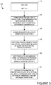
- Fig. 3 An example method for minimizing this function according to embodiments of the invention is illustrated in Fig. 3 .
- the equation (25) is used to find a value for a that minimizes the difference between measured and theoretical experiment magnitudes.
- the measured values are divided by the computed value for a in an operation 130.
- the point b is set to the minimum point found above and then perform a similar search over values of c , again saving the minimum point found.
- the processes 110 - 150 of Fig. 3 are used to locate a starting point for a more accurate search.
- the processes 110 - 150 ensure that the starting point is not confused with any local minima that are not the global minima of interest.
- a process 160 is performed until exit criteria are met.
- the processes 210 - 250 alternately adjust a, then ⁇ b, c ⁇ until a ceases to change by a significant amount between steps.
- the significant amount may be a programmable setting. Due to the problem structure, an incorrect value for a will result in c iterating to the wrong value.
- a is permanently set to unity and the measurements m ⁇ are scaled instead.
- equation (25) is used to find a value for a which minimizes the difference between measured and theoretical experiment magnitudes. Then, in an operation 220, measured values are divided by the a value thus computed. Then, an operation 220 first numerically estimates first and second derivatives, and then uses Simpson's rule to iteratively find the zero point of the first derivative within some desired tolerance. The tolerance may be set to a predetermined value. In an operation 230, the search point is replaced with the value thus derived.
- An operation 250 causes the flow 200 to repeat operations 210 - 240 to compute a new adjustment to a .
- this adjustment is sufficiently close to one ( e.g., 1 ⁇ 10 -6 ) the method has determined the correct result magnitude and the values of ⁇ b, c ⁇ .
- An operation 260 outputs the amount of IQ imbalance present.
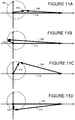
- FIG. 7 shows these experiments as a phasor diagram. This set of experiments consists of three test signals:
- Fig. 8 shows the experiment with the large outer triangle's sides and angles labeled with letters a,b,c ; small letters for the sides and capital letters for the angles. From the experiments, the lengths of the three sides are known:
- the length of the I vector (aka c 2 ) can be found with the law of cosines. From there the law of sines can be used to find the angle between I and Q ( A 2 ) .
- equations (34), (35), (36), and (37) are used to find the lengths of the I and Q vectors, and the angle between them.
- each test will generate a signal whose magnitude is exactly one tenth of the magnitude of the baseband modulation signals.
- the four resulting output signals 670 in Figs. 10A - 10D will (ideally) be equal in amplitude and spaced 90-degrees apart in phase. Essentially, this has sampled four equally-spaced points around a circle 690 centered on the origin (shown as a dotted line in Figs. 10A-10D ).
- signal 610 represents the I vector multiplied by ⁇ , which is one for all four test cases in (38).
- the resulting output signal, 670 has a magnitude equal to one tenth of the I vector's magnitude and is in phase with the I vector.
- the resulting modulated sideband amplitudes are roughly ten times more sensitive to relative magnitude and phase errors between I and Q. As a result, measurement accuracies of 0.09 and 0.026dB are sufficient to achieve 60 to 70dB of sideband rejection.
- Figs. 11A - 11D show the effect of I-Q imbalance on this experiment, especially when contrasted to their analogues of Figs. 10A - 10D .
- the experiment of test signals is designed to sample points on a circle 790 with radius equal to 10% of the I vector's length.
- the actual circle illustrate has a radius equal to 10% of the errant Q vector's length.
- test frequencies may wind up combining with some of the intended test signals and further polluting the measurement results. This can be avoided by judicious choice of test frequencies. In some cases such a choice limits the number of test frequencies that can be produced and requires a non-uniform distribution.
- a good measure of the accuracy of these methods is the amount of resulting sideband suppression obtained by applying corrections for the estimated amplitude and phase errors.
- sideband suppression ratios of at least 60dB were consistently obtained.
- Fig. 12 is a functional block diagram illustrating components of a measuring device 900 for determining IQ imbalance according to embodiments of the invention.
- an IQ modulator for testing is illustrated as 820, which has two baseband inputs x and y.
- the baseband inputs may also be modified by a pre-distorter 810 as described below. If the pre-distorter 810 modifies the baseband inputs x and y, then it is modified baseband inputs x' and y' that are input to the IQ modulator 820.
- Test signals are provided by a test signal generator 930 of the IQ imbalance measuring device 900. Test signals are described in detail above. When applied to the baseband inputs x and y (or x' and y'), the IQ modulator 820 generates output specifically stimulated by the test signals, which may be measured by a frequency selective measurement device 830, such as a frequency analyzer or spectrum analyzer.
- a frequency selective measurement device 830 such as a frequency analyzer or spectrum analyzer.
- the output from the spectrum analyzer 830 is fed into the imbalance measuring device 900 and the output is analyzed 910 according to the above-described methods.
- a minimization process 920 instructs the test signal generator 930 to modify the set of test signals so that a new output from the new test signals may be measured. This repeats until a minimum test signal set, or factors of the test signal, are minimized.
- a measurement of imbalance of the IQ modulator 820 may be separately output from the measurer 900.
- a corrector processor 940 may generate codes, such as filter parameters or other data to be sent to the pre-distorter 810 so that any effects of the measured IQ imbalance may be minimized.
- the baseband inputs x and y may be modified in the pre-distorter 810, and one of the reasons for such modification may be to reduce the effects of the IQ imbalance of the modulator 820 being tested.
- the illustrated embodiments may be modified in arrangement and detail without departing from such principles, and may be combined in any desired manner.
- the foregoing discussion has focused on particular embodiments, other configurations are contemplated. In particular, even though expressions such as "according to an embodiment of the invention” or the like are used herein, these phrases are meant to generally reference embodiment possibilities, and are not intended to limit the invention to particular embodiment configurations.
Landscapes
- Engineering & Computer Science (AREA)
- Computer Networks & Wireless Communication (AREA)
- Signal Processing (AREA)
- Digital Transmission Methods That Use Modulated Carrier Waves (AREA)
Claims (8)
- Procédé de détermination de déséquilibre IQ dans un modulateur IQ (5) possédant un canal I et un canal Q, ledit procédé comprenant :l'application d'un ensemble d'au moins trois signaux d'essai au canal I et au canal Q du modulateur IQ afin de générer une sortie du modulateur IQ, au moins l'un dudit ensemble de signaux d'essai étant différent des autres signaux d'essai dudit ensemble, et lesdits signaux d'essai étant des combinaisons linéaires différentes des vecteurs I et Q ;la réception d'une sortie spécifique à la fréquence provenant d'un dispositif de mesure de fréquence couplé à la sortie du modulateur IQ ;pour chaque combinaison linéaire, la prise de mesure d'une ou de plusieurs valeurs de la sortie spécifique à la fréquence en mesurant l'amplitude d'une bande latérale ; et caractérisé par la dérivation du déséquilibre dans le modulateur IQ à partir des valeurs mesurées en définissant les vecteurs I et Q sous la forme I = a et Q = a (b + jc) et en utilisant un algorithme d'optimisation pour trouver {a, b, c} de sorte qu'une distance entre les amplitudes théoriques et les valeurs mesurées soit minimisée.
- Procédé de détermination de déséquilibre IQ dans un modulateur IQ selon la revendication 1, ladite prise de mesure d'une ou de plusieurs valeurs de la sortie spécifique à la fréquence comprenant le calcul d'une distance, ledit procédé comprenant en outre :l'ajustement des au moins trois signaux d'essai dans l'ensemble des signaux d'essai jusqu'à ce que la distance calculée soit une distance souhaitée minimale.
- Procédé de détermination de déséquilibre IQ dans un modulateur IQ selon la revendication 2, ledit ajustement des au moins trois signaux d'essai dans l'ensemble des signaux d'essai jusqu'à ce que la distance calculée soit une distance souhaitée minimale comprenant :l'ajustement d'un facteur d'au moins un des au moins trois signaux d'essai dudit l'ensemble jusqu'à ce que la distance calculée ne soit pas modifiée au-delà d'une quantité seuil lorsque le facteur est ajusté d'une quantité inférieure à une quantité seuil.
- Procédé de détermination de déséquilibre IQ dans un modulateur IQ selon la revendication 1, ladite prise de mesure d'une ou de plusieurs valeurs de la sortie spécifique à la fréquence comprenant : la prise de mesure d'une amplitude d'un signal de bande latérale.
- Procédé de détermination de déséquilibre IQ dans un modulateur IQ selon la revendication 1, ladite dérivation du déséquilibre dans le modulateur IQ à partir des valeurs mesurées comprenant :la détermination de la longueur d'un vecteur I ;la détermination de la longueur d'un vecteur Q ; etle calcul de l'angle entre le vecteur I et le vecteur Q.
- Procédé de détermination de déséquilibre IQ dans un modulateur IQ selon la revendication 1, ledit ensemble d'au moins trois signaux d'essai comprenant un ensemble de quatre signaux d'essai, et dans lequel une sortie de chacun des signaux de l'ensemble des quatre signaux d'essai serait égale en amplitude et espacée de 90 degrés en phase si le modulateur IQ était un modulateur idéal.
- Procédé de détermination de déséquilibre IQ dans un modulateur IQ selon la revendication 6, comprenant en outre l'application de l'ensemble d'au moins quatre signaux d'essai à un modulateur IQ non idéal.
- Procédé de détermination de déséquilibre IQ dans un modulateur IQ selon la revendication 1, ledit ensemble des signaux d'essai comprenant au moins un signal d'essai comprenant plusieurs fréquences simultanées.
Applications Claiming Priority (1)
| Application Number | Priority Date | Filing Date | Title |
|---|---|---|---|
| US13/683,102 US8873608B2 (en) | 2012-11-21 | 2012-11-21 | Measurement of IQ imbalance in a vector modulator |
Publications (3)
| Publication Number | Publication Date |
|---|---|
| EP2736211A2 EP2736211A2 (fr) | 2014-05-28 |
| EP2736211A3 EP2736211A3 (fr) | 2016-03-09 |
| EP2736211B1 true EP2736211B1 (fr) | 2017-10-25 |
Family
ID=49916799
Family Applications (1)
| Application Number | Title | Priority Date | Filing Date |
|---|---|---|---|
| EP13193812.8A Active EP2736211B1 (fr) | 2012-11-21 | 2013-11-21 | Mesure du déséquilibre IQ dans un modulateur de vecteur |
Country Status (4)
| Country | Link |
|---|---|
| US (1) | US8873608B2 (fr) |
| EP (1) | EP2736211B1 (fr) |
| JP (1) | JP6689558B2 (fr) |
| CN (1) | CN103840896B (fr) |
Families Citing this family (4)
| Publication number | Priority date | Publication date | Assignee | Title |
|---|---|---|---|---|
| US9397761B2 (en) | 2013-05-17 | 2016-07-19 | Crfs Limited | RF signal generating device |
| CN105847198B (zh) * | 2016-03-15 | 2018-11-09 | 东南大学 | Ofdm-wlan射频测试系统的iq不平衡估计与补偿方法 |
| JP6786404B2 (ja) * | 2017-01-11 | 2020-11-18 | Kddi株式会社 | 送信装置、受信装置、通信システム及び通信方法 |
| KR102055192B1 (ko) * | 2017-08-25 | 2019-12-12 | 한밭대학교 산학협력단 | 직접 변환 송신기의 i/q 불균형 보상 장치 및 방법 |
Citations (2)
| Publication number | Priority date | Publication date | Assignee | Title |
|---|---|---|---|---|
| US20030095607A1 (en) * | 2001-10-16 | 2003-05-22 | Xinping Huang | System and method for direct transmitter self-calibration |
| US20090270053A1 (en) * | 2004-12-16 | 2009-10-29 | Koninklijke Philips Electronics N.V. | Calibrating amplitude and phase imbalance and dc offset of an analog i/q modulator in a high-frequency transmitter |
Family Cites Families (18)
| Publication number | Priority date | Publication date | Assignee | Title |
|---|---|---|---|---|
| FR2785111B1 (fr) * | 1998-10-23 | 2004-08-20 | St Microelectronics Sa | Procede et systeme de reglage du niveau des raies parasites du spectre frequentiel de sortie d'un dispositif de transposition de frequence a bande laterale unique, en particulier incorpore dans un telephone mobile |
| US6940916B1 (en) * | 2000-01-27 | 2005-09-06 | Pmc-Sierra, Inc. | Wideband analog quadrature modulator/demodulator with pre-compensation/post-compensation correction |
| DE60031242T2 (de) * | 2000-05-09 | 2007-02-01 | Alcatel | Verfahren zur Steuerung des Senders in einem Funksendeempfänger und der entsprechende Funksendeempfänger |
| US7242728B2 (en) * | 2002-05-24 | 2007-07-10 | Anritsu Corporation | Quadrature modulator carrier quadrature error detection method and quadrature modulation device |
| US20040165678A1 (en) * | 2002-08-27 | 2004-08-26 | Zivi Nadiri | Method for measuring and compensating gain and phase imbalances in quadrature modulators |
| JP4166064B2 (ja) * | 2002-09-27 | 2008-10-15 | 三洋電機株式会社 | 無線装置、iq信号調整方法、およびiq信号調整プログラム |
| US7180937B2 (en) * | 2002-11-20 | 2007-02-20 | Agilent Technologies, Inc. | Method for determining imbalance in a vector signal modulator |
| US7139536B2 (en) * | 2003-12-02 | 2006-11-21 | Mediatek Inc. | Method and apparatus for I/Q imbalance calibration of a transmitter system |
| US8184740B2 (en) * | 2006-04-21 | 2012-05-22 | Nec Corporation | Signal processing circuit |
| US8654885B2 (en) * | 2006-06-06 | 2014-02-18 | Qualcomm Incorporated | Fast in-phase and quadrature imbalance calibration |
| US7856050B1 (en) * | 2007-08-15 | 2010-12-21 | L-3 Communications Titan Corporation | Receiver and transmitter calibration to compensate for frequency dependent I/Q imbalance |
| US8000382B2 (en) * | 2008-01-04 | 2011-08-16 | Qualcomm Incorporated | I/Q imbalance estimation and correction in a communication system |
| CN101610090B (zh) * | 2008-06-20 | 2012-10-10 | 大唐移动通信设备有限公司 | 一种零中频发射机和校准零中频发射信号的方法 |
| KR101238877B1 (ko) * | 2009-06-30 | 2013-03-05 | (주)에프씨아이 | 아이큐 임밸런스 추정 및 보상 방법 |
| CN102377700B (zh) * | 2010-08-18 | 2014-06-11 | 上海明波通信技术有限公司 | 估计发送端和接收端i/q不平衡的方法 |
| CN102340479B (zh) * | 2011-10-25 | 2014-04-02 | 北京华力创通科技股份有限公司 | Iq不平衡补偿装置和方法 |
| CN102437983B (zh) * | 2011-10-27 | 2015-05-06 | 安徽省菲特科技股份有限公司 | 发射端i/q调制不平衡自校正方法及装置 |
| US8442150B1 (en) * | 2012-02-24 | 2013-05-14 | National Instruments Corporation | Measurement of transmitter impairments using offset local oscillators |
-
2012
- 2012-11-21 US US13/683,102 patent/US8873608B2/en active Active
-
2013
- 2013-11-20 CN CN201310757258.1A patent/CN103840896B/zh active Active
- 2013-11-21 JP JP2013241116A patent/JP6689558B2/ja active Active
- 2013-11-21 EP EP13193812.8A patent/EP2736211B1/fr active Active
Patent Citations (2)
| Publication number | Priority date | Publication date | Assignee | Title |
|---|---|---|---|---|
| US20030095607A1 (en) * | 2001-10-16 | 2003-05-22 | Xinping Huang | System and method for direct transmitter self-calibration |
| US20090270053A1 (en) * | 2004-12-16 | 2009-10-29 | Koninklijke Philips Electronics N.V. | Calibrating amplitude and phase imbalance and dc offset of an analog i/q modulator in a high-frequency transmitter |
Also Published As
| Publication number | Publication date |
|---|---|
| CN103840896A (zh) | 2014-06-04 |
| JP6689558B2 (ja) | 2020-04-28 |
| EP2736211A2 (fr) | 2014-05-28 |
| CN103840896B (zh) | 2017-09-29 |
| JP2014103672A (ja) | 2014-06-05 |
| US20140140382A1 (en) | 2014-05-22 |
| US8873608B2 (en) | 2014-10-28 |
| EP2736211A3 (fr) | 2016-03-09 |
Similar Documents
| Publication | Publication Date | Title |
|---|---|---|
| EP1514393B1 (fr) | Compensation de desequilibre d'amplitude d'un modulateur en quadrature | |
| EP0503588B1 (fr) | Modulateur d'amplitude en quadrature, avec compensation des distorsions | |
| US7010278B2 (en) | Sideband suppression method and apparatus for quadrature modulator using magnitude measurements | |
| CN102843321B (zh) | Iq不平衡补偿装置及方法 | |
| US8090011B2 (en) | Measuring apparatus, measuring method, recording medium, and test apparatus | |
| JP3826147B2 (ja) | デジタル直角変調器 | |
| US8976914B2 (en) | Multi-tap IQ imbalance estimation and correction circuit and method | |
| US20040165678A1 (en) | Method for measuring and compensating gain and phase imbalances in quadrature modulators | |
| US9780891B2 (en) | Method and device for calibrating IQ imbalance and DC offset of RF tranceiver | |
| EP2501091A2 (fr) | Système de modulation en quadrature | |
| EP2736211B1 (fr) | Mesure du déséquilibre IQ dans un modulateur de vecteur | |
| US7760817B2 (en) | Communication system for utilizing single tone testing signal having specific frequency or combinations of DC value and single tone testing signal to calibrate impairments in transmitting signal | |
| US10225118B1 (en) | Carrier leakage correction method for quadrature modulator | |
| US6512800B1 (en) | Method and system for correcting phase and amplitude imbalances of a quadrature modulated RF signal | |
| EP2770632B1 (fr) | Mesure de décalages CC dans des modulateurs IQ | |
| JP4106370B2 (ja) | 直交変調装置の校正方法、直交変調装置および無線端末試験装置 | |
| US11268997B1 (en) | Method and apparatus for characterizing homodyne transmitters and receivers | |
| EP2339755A1 (fr) | Compensation de la gigue d'horloge | |
| US20120300876A1 (en) | Quadrature modulator, signal generating device, and quadrature modulation method | |
| US8164322B2 (en) | Phase-difference-corresponding-value measurement device, gain imbalance measurement device, method, program, and recording medium | |
| EP4589851A1 (fr) | Procédé de correction d'erreurs dans un système de génération de signal iq | |
| EP4589850A1 (fr) | Procédé de suppression de parties de signal indésirables dans un signal iq | |
| US20250192812A1 (en) | Phase characteristic measurement device, signal generator and signal analyzer having same, and phase characteristic measurement method | |
| US8913693B2 (en) | Quadrature modulator balancing system |
Legal Events
| Date | Code | Title | Description |
|---|---|---|---|
| PUAI | Public reference made under article 153(3) epc to a published international application that has entered the european phase |
Free format text: ORIGINAL CODE: 0009012 |
|
| 17P | Request for examination filed |
Effective date: 20131121 |
|
| AK | Designated contracting states |
Kind code of ref document: A2 Designated state(s): AL AT BE BG CH CY CZ DE DK EE ES FI FR GB GR HR HU IE IS IT LI LT LU LV MC MK MT NL NO PL PT RO RS SE SI SK SM TR |
|
| AX | Request for extension of the european patent |
Extension state: BA ME |
|
| RAP1 | Party data changed (applicant data changed or rights of an application transferred) |
Owner name: TEKTRONIX, INC. |
|
| PUAL | Search report despatched |
Free format text: ORIGINAL CODE: 0009013 |
|
| AK | Designated contracting states |
Kind code of ref document: A3 Designated state(s): AL AT BE BG CH CY CZ DE DK EE ES FI FR GB GR HR HU IE IS IT LI LT LU LV MC MK MT NL NO PL PT RO RS SE SI SK SM TR |
|
| AX | Request for extension of the european patent |
Extension state: BA ME |
|
| RIC1 | Information provided on ipc code assigned before grant |
Ipc: H04L 27/36 20060101AFI20160202BHEP Ipc: H04B 1/62 20060101ALI20160202BHEP |
|
| R17P | Request for examination filed (corrected) |
Effective date: 20160906 |
|
| RBV | Designated contracting states (corrected) |
Designated state(s): AL AT BE BG CH CY CZ DE DK EE ES FI FR GB GR HR HU IE IS IT LI LT LU LV MC MK MT NL NO PL PT RO RS SE SI SK SM TR |
|
| 17Q | First examination report despatched |
Effective date: 20161214 |
|
| GRAP | Despatch of communication of intention to grant a patent |
Free format text: ORIGINAL CODE: EPIDOSNIGR1 |
|
| INTG | Intention to grant announced |
Effective date: 20170518 |
|
| GRAS | Grant fee paid |
Free format text: ORIGINAL CODE: EPIDOSNIGR3 |
|
| GRAA | (expected) grant |
Free format text: ORIGINAL CODE: 0009210 |
|
| AK | Designated contracting states |
Kind code of ref document: B1 Designated state(s): AL AT BE BG CH CY CZ DE DK EE ES FI FR GB GR HR HU IE IS IT LI LT LU LV MC MK MT NL NO PL PT RO RS SE SI SK SM TR |
|
| REG | Reference to a national code |
Ref country code: GB Ref legal event code: FG4D |
|
| REG | Reference to a national code |
Ref country code: CH Ref legal event code: EP |
|
| REG | Reference to a national code |
Ref country code: AT Ref legal event code: REF Ref document number: 940884 Country of ref document: AT Kind code of ref document: T Effective date: 20171115 |
|
| REG | Reference to a national code |
Ref country code: IE Ref legal event code: FG4D |
|
| REG | Reference to a national code |
Ref country code: DE Ref legal event code: R096 Ref document number: 602013028336 Country of ref document: DE |
|
| REG | Reference to a national code |
Ref country code: NL Ref legal event code: MP Effective date: 20171025 |
|
| REG | Reference to a national code |
Ref country code: LT Ref legal event code: MG4D |
|
| REG | Reference to a national code |
Ref country code: AT Ref legal event code: MK05 Ref document number: 940884 Country of ref document: AT Kind code of ref document: T Effective date: 20171025 |
|
| PG25 | Lapsed in a contracting state [announced via postgrant information from national office to epo] |
Ref country code: NL Free format text: LAPSE BECAUSE OF FAILURE TO SUBMIT A TRANSLATION OF THE DESCRIPTION OR TO PAY THE FEE WITHIN THE PRESCRIBED TIME-LIMIT Effective date: 20171025 |
|
| PG25 | Lapsed in a contracting state [announced via postgrant information from national office to epo] |
Ref country code: FI Free format text: LAPSE BECAUSE OF FAILURE TO SUBMIT A TRANSLATION OF THE DESCRIPTION OR TO PAY THE FEE WITHIN THE PRESCRIBED TIME-LIMIT Effective date: 20171025 Ref country code: ES Free format text: LAPSE BECAUSE OF FAILURE TO SUBMIT A TRANSLATION OF THE DESCRIPTION OR TO PAY THE FEE WITHIN THE PRESCRIBED TIME-LIMIT Effective date: 20171025 Ref country code: NO Free format text: LAPSE BECAUSE OF FAILURE TO SUBMIT A TRANSLATION OF THE DESCRIPTION OR TO PAY THE FEE WITHIN THE PRESCRIBED TIME-LIMIT Effective date: 20180125 Ref country code: LT Free format text: LAPSE BECAUSE OF FAILURE TO SUBMIT A TRANSLATION OF THE DESCRIPTION OR TO PAY THE FEE WITHIN THE PRESCRIBED TIME-LIMIT Effective date: 20171025 Ref country code: SE Free format text: LAPSE BECAUSE OF FAILURE TO SUBMIT A TRANSLATION OF THE DESCRIPTION OR TO PAY THE FEE WITHIN THE PRESCRIBED TIME-LIMIT Effective date: 20171025 |
|
| PG25 | Lapsed in a contracting state [announced via postgrant information from national office to epo] |
Ref country code: BG Free format text: LAPSE BECAUSE OF FAILURE TO SUBMIT A TRANSLATION OF THE DESCRIPTION OR TO PAY THE FEE WITHIN THE PRESCRIBED TIME-LIMIT Effective date: 20180125 Ref country code: GR Free format text: LAPSE BECAUSE OF FAILURE TO SUBMIT A TRANSLATION OF THE DESCRIPTION OR TO PAY THE FEE WITHIN THE PRESCRIBED TIME-LIMIT Effective date: 20180126 Ref country code: IS Free format text: LAPSE BECAUSE OF FAILURE TO SUBMIT A TRANSLATION OF THE DESCRIPTION OR TO PAY THE FEE WITHIN THE PRESCRIBED TIME-LIMIT Effective date: 20180225 Ref country code: LV Free format text: LAPSE BECAUSE OF FAILURE TO SUBMIT A TRANSLATION OF THE DESCRIPTION OR TO PAY THE FEE WITHIN THE PRESCRIBED TIME-LIMIT Effective date: 20171025 Ref country code: RS Free format text: LAPSE BECAUSE OF FAILURE TO SUBMIT A TRANSLATION OF THE DESCRIPTION OR TO PAY THE FEE WITHIN THE PRESCRIBED TIME-LIMIT Effective date: 20171025 Ref country code: AT Free format text: LAPSE BECAUSE OF FAILURE TO SUBMIT A TRANSLATION OF THE DESCRIPTION OR TO PAY THE FEE WITHIN THE PRESCRIBED TIME-LIMIT Effective date: 20171025 Ref country code: HR Free format text: LAPSE BECAUSE OF FAILURE TO SUBMIT A TRANSLATION OF THE DESCRIPTION OR TO PAY THE FEE WITHIN THE PRESCRIBED TIME-LIMIT Effective date: 20171025 |
|
| REG | Reference to a national code |
Ref country code: DE Ref legal event code: R097 Ref document number: 602013028336 Country of ref document: DE |
|
| PG25 | Lapsed in a contracting state [announced via postgrant information from national office to epo] |
Ref country code: MC Free format text: LAPSE BECAUSE OF FAILURE TO SUBMIT A TRANSLATION OF THE DESCRIPTION OR TO PAY THE FEE WITHIN THE PRESCRIBED TIME-LIMIT Effective date: 20171025 Ref country code: EE Free format text: LAPSE BECAUSE OF FAILURE TO SUBMIT A TRANSLATION OF THE DESCRIPTION OR TO PAY THE FEE WITHIN THE PRESCRIBED TIME-LIMIT Effective date: 20171025 Ref country code: CH Free format text: LAPSE BECAUSE OF NON-PAYMENT OF DUE FEES Effective date: 20171130 Ref country code: CY Free format text: LAPSE BECAUSE OF FAILURE TO SUBMIT A TRANSLATION OF THE DESCRIPTION OR TO PAY THE FEE WITHIN THE PRESCRIBED TIME-LIMIT Effective date: 20171025 Ref country code: DK Free format text: LAPSE BECAUSE OF FAILURE TO SUBMIT A TRANSLATION OF THE DESCRIPTION OR TO PAY THE FEE WITHIN THE PRESCRIBED TIME-LIMIT Effective date: 20171025 Ref country code: SK Free format text: LAPSE BECAUSE OF FAILURE TO SUBMIT A TRANSLATION OF THE DESCRIPTION OR TO PAY THE FEE WITHIN THE PRESCRIBED TIME-LIMIT Effective date: 20171025 Ref country code: LI Free format text: LAPSE BECAUSE OF NON-PAYMENT OF DUE FEES Effective date: 20171130 Ref country code: CZ Free format text: LAPSE BECAUSE OF FAILURE TO SUBMIT A TRANSLATION OF THE DESCRIPTION OR TO PAY THE FEE WITHIN THE PRESCRIBED TIME-LIMIT Effective date: 20171025 |
|
| PG25 | Lapsed in a contracting state [announced via postgrant information from national office to epo] |
Ref country code: LU Free format text: LAPSE BECAUSE OF NON-PAYMENT OF DUE FEES Effective date: 20171121 Ref country code: IT Free format text: LAPSE BECAUSE OF FAILURE TO SUBMIT A TRANSLATION OF THE DESCRIPTION OR TO PAY THE FEE WITHIN THE PRESCRIBED TIME-LIMIT Effective date: 20171025 Ref country code: SM Free format text: LAPSE BECAUSE OF FAILURE TO SUBMIT A TRANSLATION OF THE DESCRIPTION OR TO PAY THE FEE WITHIN THE PRESCRIBED TIME-LIMIT Effective date: 20171025 Ref country code: RO Free format text: LAPSE BECAUSE OF FAILURE TO SUBMIT A TRANSLATION OF THE DESCRIPTION OR TO PAY THE FEE WITHIN THE PRESCRIBED TIME-LIMIT Effective date: 20171025 Ref country code: PL Free format text: LAPSE BECAUSE OF FAILURE TO SUBMIT A TRANSLATION OF THE DESCRIPTION OR TO PAY THE FEE WITHIN THE PRESCRIBED TIME-LIMIT Effective date: 20171025 |
|
| PLBE | No opposition filed within time limit |
Free format text: ORIGINAL CODE: 0009261 |
|
| REG | Reference to a national code |
Ref country code: FR Ref legal event code: ST Effective date: 20180731 Ref country code: BE Ref legal event code: MM Effective date: 20171130 |
|
| STAA | Information on the status of an ep patent application or granted ep patent |
Free format text: STATUS: NO OPPOSITION FILED WITHIN TIME LIMIT |
|
| REG | Reference to a national code |
Ref country code: IE Ref legal event code: MM4A |
|
| PG25 | Lapsed in a contracting state [announced via postgrant information from national office to epo] |
Ref country code: MT Free format text: LAPSE BECAUSE OF NON-PAYMENT OF DUE FEES Effective date: 20171121 |
|
| 26N | No opposition filed |
Effective date: 20180726 |
|
| PG25 | Lapsed in a contracting state [announced via postgrant information from national office to epo] |
Ref country code: IE Free format text: LAPSE BECAUSE OF NON-PAYMENT OF DUE FEES Effective date: 20171121 Ref country code: FR Free format text: LAPSE BECAUSE OF NON-PAYMENT OF DUE FEES Effective date: 20171226 |
|
| PG25 | Lapsed in a contracting state [announced via postgrant information from national office to epo] |
Ref country code: BE Free format text: LAPSE BECAUSE OF NON-PAYMENT OF DUE FEES Effective date: 20171130 Ref country code: SI Free format text: LAPSE BECAUSE OF FAILURE TO SUBMIT A TRANSLATION OF THE DESCRIPTION OR TO PAY THE FEE WITHIN THE PRESCRIBED TIME-LIMIT Effective date: 20171025 |
|
| PGFP | Annual fee paid to national office [announced via postgrant information from national office to epo] |
Ref country code: GB Payment date: 20181127 Year of fee payment: 6 |
|
| PG25 | Lapsed in a contracting state [announced via postgrant information from national office to epo] |
Ref country code: HU Free format text: LAPSE BECAUSE OF FAILURE TO SUBMIT A TRANSLATION OF THE DESCRIPTION OR TO PAY THE FEE WITHIN THE PRESCRIBED TIME-LIMIT; INVALID AB INITIO Effective date: 20131121 |
|
| PG25 | Lapsed in a contracting state [announced via postgrant information from national office to epo] |
Ref country code: MK Free format text: LAPSE BECAUSE OF FAILURE TO SUBMIT A TRANSLATION OF THE DESCRIPTION OR TO PAY THE FEE WITHIN THE PRESCRIBED TIME-LIMIT Effective date: 20171025 |
|
| PG25 | Lapsed in a contracting state [announced via postgrant information from national office to epo] |
Ref country code: TR Free format text: LAPSE BECAUSE OF FAILURE TO SUBMIT A TRANSLATION OF THE DESCRIPTION OR TO PAY THE FEE WITHIN THE PRESCRIBED TIME-LIMIT Effective date: 20171025 |
|
| PG25 | Lapsed in a contracting state [announced via postgrant information from national office to epo] |
Ref country code: PT Free format text: LAPSE BECAUSE OF FAILURE TO SUBMIT A TRANSLATION OF THE DESCRIPTION OR TO PAY THE FEE WITHIN THE PRESCRIBED TIME-LIMIT Effective date: 20171025 |
|
| PG25 | Lapsed in a contracting state [announced via postgrant information from national office to epo] |
Ref country code: AL Free format text: LAPSE BECAUSE OF FAILURE TO SUBMIT A TRANSLATION OF THE DESCRIPTION OR TO PAY THE FEE WITHIN THE PRESCRIBED TIME-LIMIT Effective date: 20171025 |
|
| GBPC | Gb: european patent ceased through non-payment of renewal fee |
Effective date: 20191121 |
|
| PG25 | Lapsed in a contracting state [announced via postgrant information from national office to epo] |
Ref country code: GB Free format text: LAPSE BECAUSE OF NON-PAYMENT OF DUE FEES Effective date: 20191121 |
|
| P01 | Opt-out of the competence of the unified patent court (upc) registered |
Effective date: 20230530 |
|
| PGFP | Annual fee paid to national office [announced via postgrant information from national office to epo] |
Ref country code: DE Payment date: 20251128 Year of fee payment: 13 |