EP2738818A2 - Cellule solaire et son procédé de fabrication - Google Patents
Cellule solaire et son procédé de fabrication Download PDFInfo
- Publication number
- EP2738818A2 EP2738818A2 EP13185339.2A EP13185339A EP2738818A2 EP 2738818 A2 EP2738818 A2 EP 2738818A2 EP 13185339 A EP13185339 A EP 13185339A EP 2738818 A2 EP2738818 A2 EP 2738818A2
- Authority
- EP
- European Patent Office
- Prior art keywords
- light
- solar cell
- absorption layer
- layer
- minutes
- Prior art date
- Legal status (The legal status is an assumption and is not a legal conclusion. Google has not performed a legal analysis and makes no representation as to the accuracy of the status listed.)
- Withdrawn
Links
Images


Classifications
-
- H—ELECTRICITY
- H10—SEMICONDUCTOR DEVICES; ELECTRIC SOLID-STATE DEVICES NOT OTHERWISE PROVIDED FOR
- H10F—INORGANIC SEMICONDUCTOR DEVICES SENSITIVE TO INFRARED RADIATION, LIGHT, ELECTROMAGNETIC RADIATION OF SHORTER WAVELENGTH OR CORPUSCULAR RADIATION
- H10F10/00—Individual photovoltaic cells, e.g. solar cells
- H10F10/10—Individual photovoltaic cells, e.g. solar cells having potential barriers
- H10F10/13—Photovoltaic cells having absorbing layers comprising graded bandgaps
-
- H—ELECTRICITY
- H10—SEMICONDUCTOR DEVICES; ELECTRIC SOLID-STATE DEVICES NOT OTHERWISE PROVIDED FOR
- H10F—INORGANIC SEMICONDUCTOR DEVICES SENSITIVE TO INFRARED RADIATION, LIGHT, ELECTROMAGNETIC RADIATION OF SHORTER WAVELENGTH OR CORPUSCULAR RADIATION
- H10F71/00—Manufacture or treatment of devices covered by this subclass
-
- H—ELECTRICITY
- H10—SEMICONDUCTOR DEVICES; ELECTRIC SOLID-STATE DEVICES NOT OTHERWISE PROVIDED FOR
- H10F—INORGANIC SEMICONDUCTOR DEVICES SENSITIVE TO INFRARED RADIATION, LIGHT, ELECTROMAGNETIC RADIATION OF SHORTER WAVELENGTH OR CORPUSCULAR RADIATION
- H10F71/00—Manufacture or treatment of devices covered by this subclass
- H10F71/128—Annealing
-
- H—ELECTRICITY
- H10—SEMICONDUCTOR DEVICES; ELECTRIC SOLID-STATE DEVICES NOT OTHERWISE PROVIDED FOR
- H10F—INORGANIC SEMICONDUCTOR DEVICES SENSITIVE TO INFRARED RADIATION, LIGHT, ELECTROMAGNETIC RADIATION OF SHORTER WAVELENGTH OR CORPUSCULAR RADIATION
- H10F77/00—Constructional details of devices covered by this subclass
- H10F77/10—Semiconductor bodies
- H10F77/12—Active materials
-
- H—ELECTRICITY
- H10—SEMICONDUCTOR DEVICES; ELECTRIC SOLID-STATE DEVICES NOT OTHERWISE PROVIDED FOR
- H10F—INORGANIC SEMICONDUCTOR DEVICES SENSITIVE TO INFRARED RADIATION, LIGHT, ELECTROMAGNETIC RADIATION OF SHORTER WAVELENGTH OR CORPUSCULAR RADIATION
- H10F77/00—Constructional details of devices covered by this subclass
- H10F77/10—Semiconductor bodies
- H10F77/12—Active materials
- H10F77/126—Active materials comprising only Group I-III-VI chalcopyrite materials, e.g. CuInSe2, CuGaSe2 or CuInGaSe2 [CIGS]
-
- Y—GENERAL TAGGING OF NEW TECHNOLOGICAL DEVELOPMENTS; GENERAL TAGGING OF CROSS-SECTIONAL TECHNOLOGIES SPANNING OVER SEVERAL SECTIONS OF THE IPC; TECHNICAL SUBJECTS COVERED BY FORMER USPC CROSS-REFERENCE ART COLLECTIONS [XRACs] AND DIGESTS
- Y02—TECHNOLOGIES OR APPLICATIONS FOR MITIGATION OR ADAPTATION AGAINST CLIMATE CHANGE
- Y02E—REDUCTION OF GREENHOUSE GAS [GHG] EMISSIONS, RELATED TO ENERGY GENERATION, TRANSMISSION OR DISTRIBUTION
- Y02E10/00—Energy generation through renewable energy sources
- Y02E10/50—Photovoltaic [PV] energy
- Y02E10/541—CuInSe2 material PV cells
-
- Y—GENERAL TAGGING OF NEW TECHNOLOGICAL DEVELOPMENTS; GENERAL TAGGING OF CROSS-SECTIONAL TECHNOLOGIES SPANNING OVER SEVERAL SECTIONS OF THE IPC; TECHNICAL SUBJECTS COVERED BY FORMER USPC CROSS-REFERENCE ART COLLECTIONS [XRACs] AND DIGESTS
- Y02—TECHNOLOGIES OR APPLICATIONS FOR MITIGATION OR ADAPTATION AGAINST CLIMATE CHANGE
- Y02P—CLIMATE CHANGE MITIGATION TECHNOLOGIES IN THE PRODUCTION OR PROCESSING OF GOODS
- Y02P70/00—Climate change mitigation technologies in the production process for final industrial or consumer products
- Y02P70/50—Manufacturing or production processes characterised by the final manufactured product
Definitions
- One or more embodiments of the present invention relate to a solar cell, a method of manufacturing the same, and more particularly, to a solar cell around which a surface of a light-absorption layer has improved resistance to thermal degradation, and a method of manufacturing the solar cell.
- a solar cell including a basic unit as a diode with a pn function may be classified depending on a material of a light-absorption layer therein.
- a solar cell using silicon in the light-absorption layer may be classified as either a crystalline wafer-type solar cell (monocrystalline or polycrystalline), or a thin film type (amorphous or polycrystalline) solar cell.
- Other representative solar cells are, for example, compound thin film type solar cells including a copper-indium-selenide (CuInSe 2 , CIS-based) or cadmium-tellurium (CdTe)-based light-absorption layer, Group III-V solar cells, dye-sensitive solar cells, and organic solar cells.
- the solar cell including a CIS-based light-absorption layer has an energy band gap (E g ) of about 1.04eV, a high short-circuit current, and a low open-circuit voltage, and thus have a low efficiency. Accordingly, there has been much research into partial substitution of Se with S for increasing the open-circuit voltage of the solar cell while maintaining adhesion between the CIS-based light-absorption layer and a rear electrode layer.
- E g energy band gap
- One or more embodiments of the present invention include a solar cell that has an improved open-circuit voltage while maintaining adhesion between a light-absorption layer and a rear-electrode layer thereof, and that has improved resistance to thermal degradation of around a surface of the light-absorption layer.
- One or more embodiments of the present invention provide a method of manufacturing the solar cell.
- the present invention provides a solar cell as claimed in any of claims 1 to 11 and a process for manufacturing said solar cell as claimed in claim 12.
- a solar cell includes:
- the depth t may preferably be no greater than about 400 nm.
- the depletion region of the light-absorption layer may have an average composition represented by Formula 1 below: ⁇ Formula 1> Cu(In 1-x Ga x )(Se 1-y S y ) 2
- x is 0.01 ⁇ x ⁇ 0.25, and y is 0.1 ⁇ y ⁇ 0.30.
- a method of manufacturing a solar cell includes:
- the light-absorption layer of the solar cell may include a depletion region ranging from a surface thereof to a depth t, and an average S/(Se+S) mole ratio in the depletion region may be from about 0.10 to about 0.30.
- a light-absorption layer includes a depletion region ranging from a surface thereof to a depth t, wherein an average S/(Se+S) mole ratio in the depletion region is in the range from about 0.10 to about 0.30.
- a solar cell including the light-absorption layer may have an improved open-circuit voltage while maintaining adhesion between the light-absorption layer and a rear electrode layer, and may have improved resistance to thermal degradation.
- FIG. 1 is a schematic view of a solar cell 600 according to an embodiment of the present invention.
- the solar cell 600 includes a rear electrode layer 200 disposed on a substrate 100, a light-absorption layer 300 disposed on the rear electrode layer 200, a buffer layer 400 disposed on the light-absorption layer 300, and a transmissive electrode layer 500 disposed on the buffer layer 400.
- the substrate 100 may include a glass, ceramic, stainless steel, metal, or polymer substrate.
- the glass substrate may be a sodalime glass or a high-strained point soda glass.
- the glass substrate may be formed of, for example, low-iron tempered glass.
- the low-iron sodalime glass may elute sodium (Na) ions at a process temperature of, for example, over about 500°C, thereby further improve efficiency of the light-absorption layer 300.
- the ceramic substrate may be, for example, an alumina substrate.
- the metal substrate may be a copper tape or the like.
- the polymer substrate may be a polyimide substrate or the like.
- the rear electrode layer 200 may include molybdenum (Mo), aluminum (Al), copper (Cu), or an alloy thereof.
- the rear electrode layer 200 may be formed of a metal material with high conductivity and high light reflectivity to be able to collect charges generated due to a photoelectric effect and to reflect light passing through the light-absorption layer 300 to be reabsorbed by the light-absorption layer 300.
- the rear electrode layer 200 may include molybdenum (Mo), in consideration of high conductivity, ohmic contact with the light-absorption layer 300, and high-temperature stability in a selenium (Se) atmosphere.
- the rear electrode layer 200 may have a thickness of from about 200 nm to about 500 nm.
- the rear electrode layer 200 may be doped with alkali ions, for example, Na ions.
- alkali ions for example, Na ions.
- the alkali ions doped on the rear electrode layer 200 may be incorporated into the light-absorption layer 300, and thus provide a structurally advantageous effect and high conductivity to the light-absorption layer 300. Accordingly, the solar cell 600 may have an increased open-circuit voltage V oc and an increased efficiency.
- the rear electrode layer 200 may be formed as a multi-layer to ensure adhesion to the substrate 100 and satisfactory resistance characteristics of the rear electrode layer 200.
- the light-absorption layer 300 as a p-type semiconductor layer including a copper-indium-gallium-selenide (Cu(In, Ga)Se 2 , CIGS)-based compound obtained by substituting part of indium (In) in a copper-indium-selenium based compound with an amount of gallium (Ga) and part of selenium (Se) with an amount of S, absorbs incident solar light.
- a copper-indium-gallium-selenide Cu(In, Ga)Se 2 , CIGS
- the light-absorption layer 300 may form a depletion region ranging from a surface thereof to a depth t.
- An average S/(Se+S) mole ratio in the depletion region may be from about 0.1 to about 0.30, and in some embodiments, from about 0.10 to about 0.27, and in some other embodiments, preferably 0.10 to about 0.30, from about 0.12 to about 0.27, from about 0.10 to about 0.25, from about 0.14 to about 0.25, from about 0.15 to about 0.25, from about 0.16 to about 0.25 or from about 0.20 to about 0.25.
- the S/(Se+S) mole ratio may be highest on the surface of the light-absorption layer 300, and may gradually reduce toward the depletion region away from the surface.
- the depth t may vary depending on the content of S.
- the depth t may be no greater than about 400 nm, for example, no greater than about 300 nm, optionally 25 to 350 nm, optionally 50 to 325 nm, optionally 250 to 325 nm.
- the light-absorption layer 300 may include a depletion region (denoted by slash lines) ranging from a surface thereof to a depth t.
- a depletion region denoted by slash lines
- a deep defect may be caused when external heat is applied to the depletion region. This may hinder collecting carriers and cause severe thermal degradation.
- the average S/(Se+S) mole ratio in the depletion region (denoted by slash lines) is within these range by controlling the content of S, adhesion between the light-absorption layer 300 and the rear electrode layer 200 may be maintained, and allows the rear electrode layer 200 to have a required minimum thickness or greater thickness for adhesion between the light-absorption layer 300 and the rear electrode layer 200.
- the light-absorption layer 300 may also have an increased surface energy band gap (E g ) and an improved open-circuit voltage V oc . Accordingly, the solar cell 600 including the light-absorption layer 300 may have improved resistance to thermal degradation.
- the depletion region (denoted by slash lines) of the light-absorption layer 300 may have an average composition represented by Formula 1 below: ⁇ Formula 1> Cu(In 1-x Ga x )(Se 1-y S y ) 2
- an average S/(Se+S) mole ratio may be from about 0.1 to about 0.30, and an average Ga/(In+Ga) mole ratio may be from about 0.01 to about 0.25.
- an average S/(Se+S) mole ratio is preferably from about 0.12 to about 0.27, from about 0.10 to about 0.25, from about 0.14 to about 0.25, from about 0.15 to about 0.25, from about 0.16 to about 0.25 or from about 0.20 to about 0.25.
- an average Ga/(In+Ga) mole ratio is preferably from about 0.01 to about 0.20.
- the average Ga/(In+Ga) mole ratio in the depletion region of the light-absorption layer 400 when the average S/(Se+S) mole ratio in the depletion region of the light-absorption layer 400 is from about 0.1 to about 0.27, the average Ga/(In+Ga) mole ratio may be from about 0.01 to about 0.27. In some other embodiments, when the average S/(Se+S) mole ratio in the depletion region of the light-absorption layer 400 is from about 0.1 to about 0.25, the average Ga/(In+Ga) mole ratio may be from about 0.01 to about 0.2.
- the light-absorption layer 300 may preferably have a thickness of from between 0.7 ⁇ m to about 2.5 ⁇ m in thickness, optionally 0.7 ⁇ m to about 2 ⁇ m and optionally 1.0 ⁇ m to about 2 ⁇ m.
- the light-absorption layer 300 may have any thickness within this range.
- the buffer layer 400 may include CdS, ZnS, ZnO, ZnSe, In 2 S 3 , Zn x Mg (1x) O (where 0 ⁇ x ⁇ 1), Zn(S, O), or Zn(S, O, OH).
- the buffer layer 400 may reduce a band gap difference between the light-absorption layer 300, and the transmissive electrode layer 500, which will be described later, and may less likely cause recombination of electrons and holes in an interface between the light-absorption layer 300 and the transmissive electrode layer 500.
- the transmissive electrode layer 500 may include ZnO, ZnO:Al, ZnO:B, indium tin oxide (ITO), or indium zinc oxide (IZO).
- the transmissive electrode layer 500 may be formed of a transparent conductive material and capture charges generated due to a photoelectric effect.
- an upper surface of the transmissive electrode layer 500 may be textured to reduce reflection of incident solar light and increase light absorption into the light-absorption layer 300.
- the present invention also provides a solar cell as defined above, wherein the solar cell is produced by a process comprising the steps of:
- the sulfurization step is carried out at a temperature of from about 525°C to about 575°C, optionally from about 540°C to about 560°C.
- the selenized metal precursor is formed by thermally treating a metal precursor layer in a H2Se atmosphere at a temperature of from about 400°C to about 480°C for selenization, optionally from about 410°C to about 450°C, for 5 minutes to about 40 minutes, optionally about 15 minutes to about 25 minutes.
- the present invention also provides a process as defined above.
- a method of manufacturing a solar cell includes: preparing a substrate with a rear electrode layer thereon; forming a light-absorption layer including Cu, In, Ga, Se, and S on the substrate with the rear electrode layer; forming a buffer layer on the light-absorption layer; and forming a transmissive electrode layer on the buffer layer, wherein the forming of the light-absorption layer involves thermally treating a metal precursor layer in a H 2 Se atmosphere at a temperature of from about 400°C to about 480°C for selenization, and thermally treating the selenized metal precursor in a H 2 S atmosphere at a temperature of from about 500°C to about 600°C for about 30 minutes to about 60 minutes for sulfurization.
- a substrate 100 with a rear electrode layer 200 is prepared.
- the rear electrode layer 200 may be formed, for example, by coating a conductive paste on the substrate 100 and thermally treating the same, or by plating.
- the rear electrode layer 200 may be formed by sputtering using a molybdenum (Mo) target.
- the light-absorption layer 300 including Cu, In, Ga, Se, and S is formed on the substrate 100 with the rear electrode layer 200 formed thereon.
- the light-absorption layer 300 may formed by co-evaporation in which copper (Cu), indium (In), gallium (Ga), and selenium (Se) are placed in an electric furnace in a vacuum chamber and then heated to evaporate
- the light-absorption layer 300 may be formed by sputtering/selenization. According to this method, a CIG-based metal precursor layer is formed on the rear electrode layer 200 using copper (Cu), indium (In), and gallium (Ga) metal targets and/or an alloy target thereof, and then thermally treated in a H 2 Se gas atmosphere to form a selenized metal precursor layer, which is then further thermally treated in a H 2 S gas atmosphere to form the light-absorption layer 300 including Cu, In, Ga, Se, and S.
- the light-absorption layer 300 may be formed by electro-deposition, molecular organic chemical vapor deposition (MOCVD), or the like.
- forming the light-absorption layer 300 by sputtering/selenization may involve thermally treating a metal precursor layer in a H 2 Se atmosphere at a temperature of from about 400°C to about 480°C for selenization, and thermally treating the selenized metal precursor layer in a H 2 S atmosphere at a temperature of from about 500°C to about 600°C for about 30 minutes to about 60 minutes for sulfurization.
- the sulfurization step is carried out at a temperature of from about 525°C to about 575°C, preferably from about 540°C to about 560°C for about 30 minutes to about 70 minutes, preferably about 30 minutes to about 60 minutes.
- the average S/(Se+S) mole ratio in the depletion region (denoted by slash lines) of the light-absorption layer 300 ranging from the surface to the depth t may be from about 0.10 to about 0.25.
- the S/(Se+S) mole ratio may be highest on the surface of the light-absorption layer 300, and may gradually reduce toward the depletion region away from the surface.
- the depth t may vary depending on the content of S.
- the depth t may be no greater than about 400 nm, for example, no greater than about 300 nm.
- the average S/(Se+S) mole ratio in the depletion region (denoted by slash lines) is within these range by controlling the content of S, adhesion between the light-absorption layer 300 and the rear electrode layer 200 may be maintained, and allows the rear electrode layer 200 to have a required minimum thickness or greater thickness for adhesion between the light-absorption layer 300 and the rear electrode layer 200.
- the light-absorption layer 300 may also have an increased surface energy band gap (E g ) and an improved open-circuit voltage V oc . Accordingly, the solar cell 600 including the light-absorption layer 300 may have improved resistance to thermal degradation.
- the depletion region of the light-absorption layer 300 may have an average composition represented by Formula 1 above.
- the light-absorption layer 300 may have a thickness of from about 0.7 ⁇ m to about 2 ⁇ m.
- the light-absorption layer 300 may have any thicknesses within this range.
- the buffer layer 400 is formed on the light-absorption layer 300.
- the buffer layer 400 may reduce a band gap difference between the p-type light-absorption layer 300 and the n-type transmissive electrode layer 500, and suppresses recombination of electrons and holes in an interface between the light-absorption layer 300 and the transmissive electrode layer 500.
- the buffer layer 400 may be formed by chemical bath deposition (CBD), atomic layer deposition (ALD), or ion lay gas reaction (ILGAR).
- the transmissive electrode layer 500 is formed on the buffer layer 400.
- the transmissive electrode layer 500 may be formed, for example, by metalorganic chemical vapor deposition (MOCVD), low-pressure chemical vapor deposition (LPCVD), or sputtering.
- MOCVD metalorganic chemical vapor deposition
- LPCVD low-pressure chemical vapor deposition
- sputtering sputtering
- a top surface of the transmissive electrode layer 500 may be processed by texturing. Texturing is to form an uneven pattern on a surface by using a physical or chemical method. When the top surface of the transmissive electrode layer 500 is processed to be rough by texturing, reflection of incident light may reduced so that the transmissive electrode layer 500 may capture a larger amount of light. This may reduce light loss.
- a sodalime glass substrate of a thickness of about 1.8 mm with a Mo rear electrode layer was prepared. Sputtering was performed using a CuGa target and an In target to form a metal precursor layer on the sodalime glass substrate with the Mo rear electrode layer.
- the metal precursor layer was subjected to selenization in a H 2 Se atmosphere at about 420°C for about 20 minutes, followed by heat treatment in a H 2 S atmosphere at about 550°C for about 60 minutes for sulfurization to form a light-absorption layer including Cu, In, Ga, Se, and S.
- the light-absorption layer formed a depletion region to a depth of about 300 nm from a surface thereof, wherein an average S/(Se+S) mole ratio in the depletion region was about 0.25.
- the light-absorption layer had a thickness of about 1.8 ⁇ m.
- a ZnS buffer layer was formed on the light-absorption layer by chemical bath deposition (CBD) using ammonia water (NH 4 OH), zinc sulfide hydrate (ZnSO 4 ⁇ 7H 2 O), and thiourea (CS(NH 2 ) 2 ).
- CBD chemical bath deposition
- NH 4 OH ammonia water
- ZnSO 4 ⁇ 7H 2 O zinc sulfide hydrate
- CS(NH 2 ) 2 thiourea
- a ZnO transmissive electrode layer was formed on the buffer layer by metal organic chemical vapor deposition (MOCVD), thereby manufacturing a solar cell.
- MOCVD metal organic chemical vapor deposition
- a sodalime glass substrate of a thickness of about 1.8 mm with a Mo rear electrode layer was prepared. Sputtering was performed using a CuGa target and an In target to form a metal precursor layer on the sodalime glass substrate with the Mo rear electrode layer.
- the metal precursor layer was subjected to selenization in a H 2 Se atmosphere at about 420°C for about 20 minutes, followed by heat treatment in a H 2 S atmosphere at about 550°C for about 50 minutes for sulfurization to form a light-absorption layer including Cu, In, Ga, Se, and S.
- the light-absorption layer formed a depletion region to a depth of about 300 nm from a surface thereof, wherein an average S/(Se+S) mole ratio in the depletion region was about 0.22.
- the light-absorption layer had a thickness of about 1.8 ⁇ m.
- a ZnS buffer layer was formed on the light-absorption layer by chemical bath deposition (CBD) using ammonia water (NH 4 OH), zinc sulfide hydrate (ZnSO 4 ⁇ 7H 2 O), and thiourea (CS(NH 2 ) 2 ).
- CBD chemical bath deposition
- NH 4 OH ammonia water
- ZnSO 4 ⁇ 7H 2 O zinc sulfide hydrate
- CS(NH 2 ) 2 thiourea
- a ZnO transmissive electrode layer was formed on the buffer layer by metal organic chemical vapor deposition (MOCVD), thereby manufacturing a solar cell.
- MOCVD metal organic chemical vapor deposition
- a sodalime glass substrate of a thickness of about 1.8 mm with a Mo rear electrode layer was prepared. Sputtering was performed using a CuGa target and an In target to form a metal precursor layer on the sodalime glass substrate with the Mo rear electrode layer.
- the metal precursor layer was subjected to selenization in a H 2 Se atmosphere at about 420°C for about 20 minutes, followed by heat treatment in a H 2 S atmosphere at about 550°C for about 30 minutes for sulfurization to form a light-absorption layer including Cu, In, Ga, Se, and S.
- the light-absorption layer formed a depletion region to a depth of about 300 nm from a surface thereof, wherein an average S/(Se+S) mole ratio in the depletion region was about 0.16.
- the light-absorption layer had a thickness of about 1.8 ⁇ m.
- a ZnS buffer layer was formed on the light-absorption layer by chemical bath deposition (CBD) using ammonia water (NH 4 OH), zinc sulfide hydrate (ZnSO 4 ⁇ 7H 2 O), and thiourea (CS(NH 2 ) 2 ).
- CBD chemical bath deposition
- NH 4 OH ammonia water
- ZnSO 4 ⁇ 7H 2 O zinc sulfide hydrate
- CS(NH 2 ) 2 thiourea
- a ZnO transmissive electrode layer was formed on the buffer layer by metal organic chemical vapor deposition (MOCVD), thereby manufacturing a solar cell.
- MOCVD metal organic chemical vapor deposition
- a sodalime glass substrate of a thickness of about 1.8 mm with a Mo rear electrode layer was prepared. Sputtering was performed using a CuGa target and an In target to form a metal precursor layer on the sodalime glass substrate with the Mo rear electrode layer.
- the metal precursor layer was subjected to selenization in a H 2 Se atmosphere at about 420°C for about 20 minutes, followed by heat treatment in a H 2 S atmosphere at about 550°C for about 20 minutes for sulfurization to form a light-absorption layer including Cu, In, Ga, Se, and S.
- the light-absorption layer formed a depletion region to a depth of about 300 nm from a surface thereof, wherein an average S/(Se+S) mole ratio in the depletion region was about 0.08.
- the light-absorption layer had a thickness of about 1.8 ⁇ m.
- a ZnS buffer layer was formed on the light-absorption layer by chemical bath deposition (CBD) using ammonia water (NH 4 OH), zinc sulfide hydrate (ZnSO 4 ⁇ 7H 2 O), and thiourea (CS(NH 2 ) 2 ).
- CBD chemical bath deposition
- NH 4 OH ammonia water
- ZnSO 4 ⁇ 7H 2 O zinc sulfide hydrate
- CS(NH 2 ) 2 thiourea
- a ZnO transmissive electrode layer was formed on the buffer layer by metal organic chemical vapor deposition (MOCVD), thereby manufacturing a solar cell.
- MOCVD metal organic chemical vapor deposition
- a sodalime glass substrate of a thickness of about 1.8 mm with a Mo rear electrode layer was prepared. Sputtering was performed using a CuGa target and an In target to form a metal precursor layer on the sodalime glass substrate with the Mo rear electrode layer.
- the metal precursor layer was subjected to selenization in a H 2 Se atmosphere at about 420°C for about 20 minutes, followed by heat treatment in a H 2 S atmosphere at about 550°C for about 110 minutes for sulfurization to form a light-absorption layer including Cu, In, Ga, Se, and S.
- the light-absorption layer formed a depletion region to a depth of about 300 nm from a surface thereof, wherein an average S/(Se+S) mole ratio in the depletion region was about 0.38.
- the light-absorption layer had a thickness of about 1.8 ⁇ m.
- a ZnS buffer layer was formed on the light-absorption layer by chemical bath deposition (CBD) using ammonia water (NH 4 OH), zinc sulfide hydrate (ZnSO 4 ⁇ 7H 2 O), and thiourea (CS(NH 2 ) 2 ).
- CBD chemical bath deposition
- NH 4 OH ammonia water
- ZnSO 4 ⁇ 7H 2 O zinc sulfide hydrate
- CS(NH 2 ) 2 thiourea
- a ZnO transmissive electrode layer was formed on the buffer layer by metal organic chemical vapor deposition (MOCVD), thereby manufacturing a solar cell.
- MOCVD metal organic chemical vapor deposition
- a sodalime glass substrate of a thickness of about 1.8 mm with a Mo rear electrode layer was prepared. Sputtering was performed using a CuGa target and an In target to form a metal precursor layer on the sodalime glass substrate with the Mo rear electrode layer.
- the metal precursor layer was subjected to selenization in a H 2 Se atmosphere at about 420°C for about 20 minutes, followed by heat treatment in a H 2 S atmosphere at about 550°C for about 90 minutes for sulfurization to form a light-absorption layer including Cu, In, Ga, Se, and S.
- the light-absorption layer formed a depletion region to a depth of about 300 nm from a surface thereof, wherein an average S/(Se+S) mole ratio in the depletion region was about 0.34.
- the light-absorption layer had a thickness of about 1.8 ⁇ m.
- a ZnS buffer layer was formed on the light-absorption layer by chemical bath deposition (CBD) using ammonia water (NH 4 OH), zinc sulfide hydrate (ZnSO 4 ⁇ 7H 2 O), and thiourea (CS(NH 2 ) 2 ).
- CBD chemical bath deposition
- NH 4 OH ammonia water
- ZnSO 4 ⁇ 7H 2 O zinc sulfide hydrate
- CS(NH 2 ) 2 thiourea
- a ZnO transmissive electrode layer was formed on the buffer layer by metal organic chemical vapor deposition (MOCVD), thereby manufacturing a solar cell.
- MOCVD metal organic chemical vapor deposition
- a sodalime glass substrate of a thickness of about 1.8 mm with a Mo rear electrode layer was prepared. Sputtering was performed using a CuGa target and an In target to form a metal precursor layer on the sodalime glass substrate with the Mo rear electrode layer.
- the metal precursor layer was subjected to selenization in a H 2 Se atmosphere at about 420°C for about 15 minutes, followed by heat treatment in a H 2 S atmosphere at about 550°C for about 90 minutes for sulfurization to form a light-absorption layer including Cu, In, Ga, Se, and S.
- the light-absorption layer formed a depletion region to a depth of about 300 nm from a surface thereof, wherein an average S/(Se+S) mole ratio in the depletion region was about 0.35.
- the light-absorption layer had a thickness of about 1.8 ⁇ m.
- a ZnS buffer layer was formed on the light-absorption layer by chemical bath deposition (CBD) using ammonia water (NH 4 OH), zinc sulfide hydrate (ZnSO 4 ⁇ 7H 2 O), and thiourea (CS(NH 2 ) 2 ).
- CBD chemical bath deposition
- NH 4 OH ammonia water
- ZnSO 4 ⁇ 7H 2 O zinc sulfide hydrate
- CS(NH 2 ) 2 thiourea
- a ZnO transmissive electrode layer was formed on the buffer layer by metal organic chemical vapor deposition (MOCVD), thereby manufacturing a solar cell.
- MOCVD metal organic chemical vapor deposition
- a sodalime glass substrate of a thickness of about 1.8 mm with a Mo rear electrode layer was prepared. Sputtering was performed using a CuGa target and an In target to form a metal precursor layer on the sodalime glass substrate with the Mo rear electrode layer.
- the metal precursor layer was subjected to selenization in a H 2 Se atmosphere at about 420°C for about 20 minutes, followed by heat treatment in a H 2 S atmosphere at about 550°C for about 100 minutes for sulfurization to form a light-absorption layer including Cu, In, Ga, Se, and S.
- the light-absorption layer formed a depletion region to a depth of about 300 nm from a surface thereof, wherein an average S/(Se+S) mole ratio in the depletion region was about 0.37.
- the light-absorption layer had a thickness of about 1.8 ⁇ m.
- a ZnS buffer layer was formed on the light-absorption layer by chemical bath deposition (CBD) using ammonia water (NH 4 OH), zinc sulfide hydrate (ZnSO 4 ⁇ 7H 2 O), and thiourea (CS(NH 2 ) 2 ).
- CBD chemical bath deposition
- NH 4 OH ammonia water
- ZnSO 4 ⁇ 7H 2 O zinc sulfide hydrate
- CS(NH 2 ) 2 thiourea
- a ZnO transmissive electrode layer was formed on the buffer layer by metal organic chemical vapor deposition (MOCVD), thereby manufacturing a solar cell.
- MOCVD metal organic chemical vapor deposition
- a sodalime glass substrate of a thickness of about 1.8 mm with a Mo rear electrode layer was prepared. Sputtering was performed using a CuGa target and an In target to form a metal precursor layer on the sodalime glass substrate with the Mo rear electrode layer.
- the metal precursor layer was subjected to selenization in a H 2 Se atmosphere at about 420°C for about 20 minutes, followed by heat treatment in a H 2 S atmosphere at about 550°C for about 80 minutes for sulfurization to form a light-absorption layer including Cu, In, Ga, Se, and S.
- the light-absorption layer formed a depletion region to a depth of about 300 nm from a surface thereof, wherein an average S/(Se+S) mole ratio in the depletion region was about 0.32.
- the light-absorption layer had a thickness of about 1.8 ⁇ m.
- a ZnS buffer layer was formed on the light-absorption layer by chemical bath deposition (CBD) using ammonia water (NH 4 OH), zinc sulfide hydrate (ZnSO 4 ⁇ 7H 2 O), and thiourea (CS(NH 2 ) 2 ).
- CBD chemical bath deposition
- NH 4 OH ammonia water
- ZnSO 4 ⁇ 7H 2 O zinc sulfide hydrate
- CS(NH 2 ) 2 thiourea
- a ZnO transmissive electrode layer was formed on the buffer layer by metal organic chemical vapor deposition (MOCVD), thereby manufacturing a solar cell.
- MOCVD metal organic chemical vapor deposition
- the solar cell of Example 1 was tested using a Raman spectrometer (available from Renishaw), in which the (depletion) region of the light-absorption layer ranging from the surface thereof to the depth of about 300 nm was irradiated with laser light of about 633 nm. The results are shown in FIG. 2 .
- CIGSe peaks appear in the range of 150cm -1 to 210cm -1
- CIGS peaks appear in the range of 275cm -1 to 340cm -1
- the depletion region of the light-absorption layer in the solar cell of Example 1 is found to have a S/(Se+S) mole ratio of about 0.25.
- the depletion region of the light-absorption layer in the solar cell of Example 1 was analyzed by secondary ion mass spectrometry (SIMS) using an analyzer (IMS-6f Magnetic Sector SIMS, available from CAMECA). The results are shown in FIG. 3 .
- the depletion region of the light-absorption layer in the solar cell of Example 1 is found to have an average S/(Se+S) mole ratio of about 0.25, and an average Ga/(In+Ga) mole ratio of about 0.08.
- the solar cells of Examples 1 to 3 were found to have lower thermal degradation rates than the solar cells of Comparative Examples 1 to 6. Although the solar cell of Comparative Example 1 had a minor difference in thermal degradation rate, i.e., about 0.2% higher, from the solar cell of Example 3, the solar cell of Comparative Example 1 had too low S/(Se+S) mole ratio as less than 0.1, and thus adhesion between the CIGS-based light-absorption layer and the rear electrode layer in the solar cell of Comparative Example 1 may be weak due to a short sulfurization time, and thus the rear electrode layer in the solar cell of Comparative Example 1 is little formed or has a very thin thickness.
- the CIGS-based light-absorption layer (300) may have a reduced surface energy band gap (Eg), which may lead to deterioration in open-circuit voltage (V oc ) characteristics.
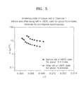
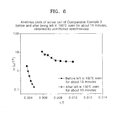
- the admittance spectroscopy test was conducted using an admittance spectrometer (B1500A, available from Agilent) in a frequency range of from 1 kHz to 1 MHz at a temperature of from about 80K to about 360K.
- B1500A admittance spectrometer
- Equation 2 ⁇ is a frequency of from 1 kHz to 1 MHz, E a indicates a defect activation energy, and ⁇ 0 indicates a pre-exponential factor as a y-intercept in the graph of FIG. 5 .)
- Example E a (meV) before and after being left in 160°C oven for 15 min Example 1 54.3, 62.3 Comparative Example 3 49.1, 242.4
- Example 1 may maintain a relatively shallow defect depth even after the exposure to external heat as compared with the solar cell of Comparative Example 3.
Landscapes
- Photovoltaic Devices (AREA)
- Engineering & Computer Science (AREA)
- Manufacturing & Machinery (AREA)
Applications Claiming Priority (2)
| Application Number | Priority Date | Filing Date | Title |
|---|---|---|---|
| US201261729513P | 2012-11-23 | 2012-11-23 | |
| US201361751219P | 2013-01-10 | 2013-01-10 |
Publications (1)
| Publication Number | Publication Date |
|---|---|
| EP2738818A2 true EP2738818A2 (fr) | 2014-06-04 |
Family
ID=49209294
Family Applications (2)
| Application Number | Title | Priority Date | Filing Date |
|---|---|---|---|
| EP13185338.4A Withdrawn EP2738817A2 (fr) | 2012-11-23 | 2013-09-20 | Cellule solaire |
| EP13185339.2A Withdrawn EP2738818A2 (fr) | 2012-11-23 | 2013-09-20 | Cellule solaire et son procédé de fabrication |
Family Applications Before (1)
| Application Number | Title | Priority Date | Filing Date |
|---|---|---|---|
| EP13185338.4A Withdrawn EP2738817A2 (fr) | 2012-11-23 | 2013-09-20 | Cellule solaire |
Country Status (3)
| Country | Link |
|---|---|
| US (2) | US20140144507A1 (fr) |
| EP (2) | EP2738817A2 (fr) |
| CN (2) | CN103840026A (fr) |
Families Citing this family (5)
| Publication number | Priority date | Publication date | Assignee | Title |
|---|---|---|---|---|
| JP6571034B2 (ja) * | 2016-03-17 | 2019-09-04 | 株式会社東芝 | 光電変換素子モジュール、太陽電池及び太陽光発電システム |
| US10062568B2 (en) * | 2016-05-13 | 2018-08-28 | Nanoco Technologies, Ltd. | Chemical vapor deposition method for fabricating two-dimensional materials |
| CN108922927B (zh) * | 2018-06-21 | 2020-07-14 | 华南师范大学 | 一种稳定的化合物半导体太阳光分解水产氢电子器件、电极系统及其制备方法 |
| CN112578298B (zh) * | 2019-09-29 | 2022-03-15 | 比亚迪股份有限公司 | 电池温度估算方法、装置、电子设备及存储介质 |
| CN118367042B (zh) * | 2024-06-20 | 2024-09-27 | 西安中易建科技集团有限公司 | 太阳能电池 |
Family Cites Families (3)
| Publication number | Priority date | Publication date | Assignee | Title |
|---|---|---|---|---|
| JP3249407B2 (ja) * | 1996-10-25 | 2002-01-21 | 昭和シェル石油株式会社 | カルコパイライト系多元化合物半導体薄膜光吸収層からなる薄膜太陽電池 |
| FR2839201B1 (fr) * | 2002-04-29 | 2005-04-01 | Electricite De France | Procede de fabrication de semi-conducteurs en couches minces a base de composes i-iii-vi2, pour applications photovoltaiques |
| US8252621B2 (en) * | 2008-02-08 | 2012-08-28 | Solopower, Inc. | Method for forming copper indium gallium chalcogenide layer with optimized gallium content at its surface |
-
2013
- 2013-09-20 US US14/033,390 patent/US20140144507A1/en not_active Abandoned
- 2013-09-20 US US14/033,406 patent/US20140144494A1/en not_active Abandoned
- 2013-09-20 EP EP13185338.4A patent/EP2738817A2/fr not_active Withdrawn
- 2013-09-20 EP EP13185339.2A patent/EP2738818A2/fr not_active Withdrawn
- 2013-11-13 CN CN201310571317.6A patent/CN103840026A/zh active Pending
- 2013-11-21 CN CN201310593814.6A patent/CN103840020A/zh active Pending
Non-Patent Citations (1)
| Title |
|---|
| None |
Also Published As
| Publication number | Publication date |
|---|---|
| US20140144507A1 (en) | 2014-05-29 |
| EP2738817A2 (fr) | 2014-06-04 |
| US20140144494A1 (en) | 2014-05-29 |
| CN103840020A (zh) | 2014-06-04 |
| CN103840026A (zh) | 2014-06-04 |
Similar Documents
| Publication | Publication Date | Title |
|---|---|---|
| US7632701B2 (en) | Thin film solar cells by selenization sulfurization using diethyl selenium as a selenium precursor | |
| Ge et al. | Synthesis and characterization of photoelectrochemical and photovoltaic Cu 2 BaSnS 4 thin films and solar cells | |
| JP6096790B2 (ja) | 光電池のための導電性基材 | |
| TWI535047B (zh) | Photoelectric conversion elements and solar cells | |
| JP2011155237A (ja) | 化合物薄膜太陽電池、化合物薄膜太陽電池の製造方法、および化合物薄膜太陽電池モジュール | |
| US8283187B2 (en) | Photovoltaic device and method for making | |
| Vermang et al. | Wide band gap kesterite absorbers for thin film solar cells: potential and challenges for their deployment in tandem devices | |
| EP2738818A2 (fr) | Cellule solaire et son procédé de fabrication | |
| EP2768030A2 (fr) | Cellule solaire et son procédé de fabrication | |
| KR20150142094A (ko) | 원자층 증착법으로 형성된 버퍼층을 포함하는 태양전지 및 이의 제조방법 | |
| KR20140066964A (ko) | 태양전지 및 이의 제조방법 | |
| KR101415251B1 (ko) | 다중 버퍼층 및 이를 포함하는 태양전지 및 그 생산방법 | |
| US20140048132A1 (en) | Solar cell and method of preparing the same | |
| JP7519053B1 (ja) | 太陽電池の製造方法及び太陽電池 | |
| US8809105B2 (en) | Method of processing a semiconductor assembly | |
| Kavitha et al. | Structural, photoelectrical characterization of Cu (InAl) Se2 thin films and the fabrication of Cu (InAl) Se2 based solar cells | |
| EP2506313A1 (fr) | Cellule solaire et procédé de fabrication de celle-ci | |
| KR101708282B1 (ko) | CZTSe계 박막을 이용한 태양전지 및 이의 제조 방법 | |
| TWI751520B (zh) | Pn接面及其製備方法及用途 | |
| US20120080306A1 (en) | Photovoltaic device and method for making | |
| EP2932802A1 (fr) | Procédés de fabrication de module photovoltaïque, et système associé | |
| JP2014107558A (ja) | 太陽電池、及び太陽電池の製造方法 | |
| EP2804220A2 (fr) | Procédé et dispositif de fabrication de cellule solaire à film mince et cellule solaire à film mince comprenant une couche tampon fabriquée par ce procédé | |
| KR101793640B1 (ko) | 인듐을 이용한 태양전지용 czts계 흡수층 박막, 이의 제조방법 및 이를 이용한 태양전지 | |
| JP2016225335A (ja) | 化合物薄膜太陽電池用基材、化合物薄膜太陽電池、化合物薄膜太陽電池モジュール、化合物薄膜太陽電池用基材の製造方法、および、化合物薄膜太陽電池の製造方法 |
Legal Events
| Date | Code | Title | Description |
|---|---|---|---|
| PUAI | Public reference made under article 153(3) epc to a published international application that has entered the european phase |
Free format text: ORIGINAL CODE: 0009012 |
|
| 17P | Request for examination filed |
Effective date: 20130920 |
|
| AK | Designated contracting states |
Kind code of ref document: A2 Designated state(s): AL AT BE BG CH CY CZ DE DK EE ES FI FR GB GR HR HU IE IS IT LI LT LU LV MC MK MT NL NO PL PT RO RS SE SI SK SM TR |
|
| AX | Request for extension of the european patent |
Extension state: BA ME |
|
| STAA | Information on the status of an ep patent application or granted ep patent |
Free format text: STATUS: THE APPLICATION IS DEEMED TO BE WITHDRAWN |
|
| 18D | Application deemed to be withdrawn |
Effective date: 20160401 |