EP2744104A2 - Automatische Verstärkungs-Steuerungseinheit für einen Empfänger oder -Sender-Empfänger mit geringer Leistungsaufnahme - Google Patents
Automatische Verstärkungs-Steuerungseinheit für einen Empfänger oder -Sender-Empfänger mit geringer Leistungsaufnahme Download PDFInfo
- Publication number
- EP2744104A2 EP2744104A2 EP13192529.9A EP13192529A EP2744104A2 EP 2744104 A2 EP2744104 A2 EP 2744104A2 EP 13192529 A EP13192529 A EP 13192529A EP 2744104 A2 EP2744104 A2 EP 2744104A2
- Authority
- EP
- European Patent Office
- Prior art keywords
- reference threshold
- control unit
- comparator
- intermediate signal
- storage capacitor
- Prior art date
- Legal status (The legal status is an assumption and is not a legal conclusion. Google has not performed a legal analysis and makes no representation as to the accuracy of the status listed.)
- Granted
Links
Images

Classifications
-
- H—ELECTRICITY
- H04—ELECTRIC COMMUNICATION TECHNIQUE
- H04B—TRANSMISSION
- H04B1/00—Details of transmission systems, not covered by a single one of groups H04B3/00 - H04B13/00; Details of transmission systems not characterised by the medium used for transmission
- H04B1/38—Transceivers, i.e. devices in which transmitter and receiver form a structural unit and in which at least one part is used for functions of transmitting and receiving
- H04B1/3827—Portable transceivers
- H04B1/3883—Arrangements for mounting batteries or battery chargers
-
- H—ELECTRICITY
- H03—ELECTRONIC CIRCUITRY
- H03G—CONTROL OF AMPLIFICATION
- H03G3/00—Gain control in amplifiers or frequency changers
- H03G3/20—Automatic control
- H03G3/30—Automatic control in amplifiers having semiconductor devices
- H03G3/3052—Automatic control in amplifiers having semiconductor devices in bandpass amplifiers (H.F. or I.F.) or in frequency-changers used in a (super)heterodyne receiver
- H03G3/3078—Circuits generating control signals for digitally modulated signals
Definitions
- the present invention relates to an automatic gain control unit for a low power receiver or transceiver.
- the automatic gain control unit can be used for a lower power FSK or PSK radiofrequency signal receiver or transceiver.
- the receiver or transceiver comprises in particular an antenna for receiving radio frequency signals, a low noise amplifier for amplifying and filtering the signals received by the antenna, a local oscillator for supplying oscillating signals, and a mixer unit for mixing the amplified incoming signals with the oscillating signals supplied by the local oscillator, in order to produce alternative intermediate signals. At least one alternative intermediate signal is processed in the automatic gain control unit.
- a receiver For the reception of radiofrequency signals, a receiver includes an automatic gain control unit, which can be used for attenuating or decreasing the gain of at least a low-noise amplifier in presence of large input signals.
- the automatic gain control unit can also be used for increasing the gain in case of low incoming signals.
- a peak detector is used in the automatic gain control loop in order to determine the signal peak level, which allows adjusting the gain of the amplifier.
- the automatic gain control unit can provide an AGC output signal in order to attenuate or not the LNA amplifier.
- the conventional automatic gain control loop with a peak detector provides low gain and require a lot of current to minimise offsets and maximize bandwidth, which is a drawback.
- the invention therefore concerns an automatic gain control unit for a low power receiver or transceiver, said receiver or transceiver comprising :
- the automatic gain control unit of the present invention lies in the fact that very low input power RF signals can be used to control said control unit.
- the radiofrequency signals can produce a peak-detected voltage on the order of the offsets of a peak detector, a digital-analogue converter and comparators. This allows the automatic gain control to be used to control a receiver in particular to meet both stringent sensitivity specifications and inter-modulation specifications, while maintaining low power consumption.
- the automatic gain control unit includes one comparator to compare at least a first alternative intermediate signal with a first reference threshold to determine the high amplitude level on the lower side or the upper side of the alternative intermediate signal.
- a comparator to compare an in-phase positive intermediate signal, an in-phase negative intermediate signal, a quarter-phase positive intermediate signal and a quarter-phase negative intermediate signal, with the first reference threshold.
- Each comparator controls a MOS transistor at output, which is connected in series with a second current source in order to discharge for example with the second current a storage capacitor, when the MOS transistor is in a conductive state. Said storage capacitor is charged with a first current from a first current source.
- an AGC output signal is supplied for an amplifier in order to attenuate or not the gain of said amplifier.
- the following description concerns specifically an automatic gain control unit for a receiver or transceiver, which can pick-up radiofrequency signals, such as FSK or PSK radiofrequency signals.
- radiofrequency signals such as FSK or PSK radiofrequency signals.
- FSK radiofrequency signal receiver which includes the automatic gain control unit, are well known in this technical field, they will be described not in detail.
- Figure 1 shows some parts of a low power radiofrequency signal receiver or transceiver 1.
- the receiver includes an antenna 2 for receiving FSK or PSK radio frequency signals, at least one low noise amplifier 3 for amplifying and filtering the signals received by the antenna.
- the receiver further includes a local oscillator 8 for supplying oscillating signals, at least one mixer unit 4 for mixing the amplified incoming signals with the oscillating signals supplied by the local oscillator to produce alternative intermediate signals.
- a mixer amplifier 5 which can produce at output alternative intermediate signals Ip, In, Qp, Qn.
- the alternative intermediate signals are composed of an in-phase positive intermediate signal Ip, an in-phase negative intermediate signal In, a quarter-phase positive intermediate signal Qp and a quarter-phase negative intermediate signal Qn. Each alternative intermediate signal are phase-shifted of 90° from each other. Said four alternative intermediate signals are based on an in-phase intermediate signal and a quarter-phase intermediate signal supplied at output of the mixer unit 4.
- the four alternative intermediate signals Ip, In, Qp, Qn are further filtered in a passband filter 6 before being supplied to a data demodulator 7.
- the four alternative intermediate signals Ip, In, Qp, Qn are supplied at input of an automatic gain control unit 10, which is used to tune the gain of the low noise amplifier 3. However it can be envisaged also to tune the gain of the IFA amplifier 5 at output of the mixer unit 4.
- the automatic gain control unit 10 supplies an AGC output signal V AGC for the LNA amplifier 3 in order to attenuate the gain of said LNA amplifier. If the amplitude level of alternative intermediate signals Ip, In, Qp, Qn is too low, the gain is adapted without attenuation, but can be considered as an increased gain relative to the step with attenuation.
- said automatic gain control unit 10 is configured for supplying an AGC output signal V AGC with two levels for attenuating or not the gain of the LNA amplifier 3.
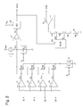
- Figure 2 shows an embodiment of the automatic gain control unit for the low-power FSK radiofrequency signal receiver.
- the automatic gain control unit includes at input four comparators 11, 12, 13, 14 to compare the four alternative intermediate signals Ip, In, Qp, Qn with at least a first reference threshold th1.
- Said first reference threshold th1 is defined for a comparison on an upper side or a lower side of the four alternative intermediate signals Ip, In, Qp, Qn.
- Said first reference threshold th1 is used to determine an amplitude level of the four alternative intermediate signals Ip, In, Qp, Qn, preferably to determine a high amplitude level.
- the determination of the amplitude level of the four alternative intermediate signals Ip, In, Qp, Qn is performed for example on the lower side. So said comparators 11, 12, 13, 14 can be considered like negative peak detectors.
- the alternative intermediate signals Ip, In, Qp, Qn have generally a sinusoidal shape.
- the amplitude of said alternative intermediate signals Ip, In, Qp, Qn does not vary during a time period for receiving FSK radiofrequency signals given that data modulation is performed by frequency shift keying (FSK) or phase shift keying (PSK).
- the oscillation of alternative intermediate signals Ip, In, Qp, Qn is defined with respect to a common mode voltage V cm corresponding to the average voltage of the alternative intermediate signals.
- the common mode voltage V cm can be around 0 V, but generally at a voltage higher than 0 V, for example at an average voltage of 0.8 V, for a supply voltage V DD from a supply voltage source for example at 1.8 V. So the upper side of the alternative intermediate signals is a positive half cycle relative to the common mode voltage or average voltage, whereas the lower side of the alternative intermediate signals is a negative half cycle relative to the common mode voltage or average voltage.
- the first reference threshold th1 is applied at the positive inputs of the first comparator 11, the second comparator 12, the third comparator 13 and the fourth comparator 14, in order to determine the high amplitude level of the alternative intermediate signals on the lower side.
- the first alternative intermediate signal which is an in-phase positive intermediate signal Ip
- the second alternative intermediate signal which is in-phase negative intermediate signal In
- the third alternative intermediate signal which is a quarter-phase positive intermediate signal Qp
- the fourth alternative intermediate signal which is a quarter-phase negative intermediate signal Qn, is applied at the negative input of the fourth comparator 14.
- the output of the first comparator 11 is connected to a gate of a first transistor N1 in order to control said first transistor N1 by a first control signal S C1 .
- the output of the second comparator 12 is connected to a gate of a second transistor N2 in order to control said second transistor N2 by a second control signal S C2 .
- the output of the third comparator 13 is connected to a gate of a third transistor N3 in order to control said third transistor N3 by a third control signal S C3 .
- the output of the fourth comparator 14 is connected to a gate of the fourth transistor N4 in order to control said fourth transistor N4 by a fourth control signal S C4 .
- the first, second, third and fourth transistors N1, N2, N3, N4 are MOS transistors, and in the embodiment shown on Figure 2 , the first, second, third and fourth transistors N1, N2, N3, N4 are NMOS transistors.
- Said first, second, third and fourth transistors N1, N2, N3, N4 are successively conductive in time when the first, second, third and fourth alternative intermediate signals Ip, In, Qp. Qn are lower than the first reference threshold th1 for a comparison on the lower side.
- Said transistors N1, N2, N3, N4 are each conductive during a time period ⁇ T within each cycle period T of the sinusoidal intermediate signals Ip, In, Qp. Qn.
- the first, second, third and fourth transistors N1, N2, N3, N4 are each connected in series with a second current source I2, which can be programmed by a binary word on 3 bits for example.
- the second current source I2 is connected to a low potential terminal of a supply voltage source for supplying a second current I2 by a source terminal of the first, second, third and fourth NMOS transistors N1, N2, N3, N4.
- a drain terminal of the first, second, third and fourth NMOS transistors N1, N2, N3, N4 are connected to a first terminal of a storage capacitor C C , whereas the second terminal of the storage capacitor is connected to the low potential terminal of the supply voltage source.
- the second current I2 is used to discharge the storage capacitor C C .
- the storage capacitor C C can be programmable by a binary word for example on 3 bits in order to adapt the capacitive value of the storage capacitor for defining a reactive time for charging or discharging said storage capacitor.
- a first current source I1 of the automatic gain control unit is connected to a high potential terminal of the supply voltage V DD in order to supply a first constant current I1 on the storage capacitor C C .
- said first current I1 is used to charge said storage capacitor C C .
- the second current I2 is supplied for discharging the storage capacitor only when the first, second, third or fourth NMOS transistors N1, N2, N3, N4 are conductive, the value of the second current I2 has to be greater than the value of the first current I1.
- the second current source I2 can be programmed to be much greater than the first current source.
- the second current value I2 can be 5 times greater than the first current value 11.
- the NMOS transistors N1, N2, N3, N4 can be conductive during 4 narrow pulses of control signals S C1 , S C2 , S C3 , S C4 if the high amplitude level of the four sinusoidal intermediate signals is greater than a level defined by the first reference threshold th1.
- the widths of all the four pulses of control signals S C1 , S C2 , S C3 , S C4 have to be greater than a value selected between 5% and 20% for example with respect to a cycle period T of the sinusoidal intermediate signals to discharge the storage capacitor C C . Preferably it can be selected a value of 20%.
- the four pulse widths correspond to the time period ⁇ T. This can be programmed also to set the AGC attack time.
- the storage capacitor C C is connected at input of a bi-stable trigger element 17, which is a Schmitt-trigger element.
- the bi-stable trigger element 17 can provide an AGC output signal depending on the voltage level on the storage capacitor for tuning the gain of the LNA amplifier or of an IFA amplifier. If the amplitude level of the alternative intermediate signals is high by having the NMOS transistors N1, N2, N3, N4 conductive during a time period greater than 20% of the cycle period T, the voltage level V CC on the storage capacitor C C becomes low after having more discharged said storage capacitor C C by the second current I2, than charged by the first current I1.
- the AGC output signal or level at output of the bi-stable trigger element 17 is high in order to attenuate the gain of the LNA amplifier or IFA amplifier by 12 dB for example. Otherwise if the NMOS transistors N1, N2, N3, N4 are conductive or not during a time period less than 20% of the cycle period T, the voltage level V CC on the storage capacitor C C is high by being charged only by the first current I1. In this case the AGC output signal or level at output of the bi-stable trigger element 17 is low in order to not attenuate the gain of the LNA amplifier or IFA amplifier.
- the automatic gain control unit can connect a RS latch 18 between the output of the bi-stable trigger element 17 and the output of said automatic gain control unit.
- Said RS latch 18 can be used to latch the output of the bi-stable trigger element 17 on the last edge in addition to allow various set modes and enables.
- Said RS latch can be reset by a signal Res in an initialisation mode or in a test mode.
- the automatic gain control unit includes also a selecting means for providing the first reference threshold th1 or a second reference threshold th2 to the four comparators 11, 12, 13, 14.
- the first reference threshold th1 is defined to detect a high amplitude level of the four alternative intermediate signals Ip, In, Qp, Qn in order to attenuate the LNA or IFA amplifier gain.
- the second reference threshold th2 is defined to detect a low amplitude level of the four alternative intermediate signals Ip, In, Qp, Qn in order to increase or not attenuate the LNA or IFA amplifier gain.
- the selecting means it is possible to generate a hysteresis in the loop to select the first or second reference threshold to prevent chatter. In principle said hysteresis can generate a gain attenuation of the 12 dB plus 3.5 dB for example.
- the selection means includes a voltage follower 15, which receives a common mode voltage V cm corresponding to the average voltage of the alternative intermediate signals Ip, In, Qp, Qn, a resistor divider connected between the output of the voltage follower 15 and the low potential terminal of the supply voltage source.
- the resistor divider is composed of at least a first resistor R1, a second resistor R2 and a third resistor R3 in series connected, with the first resistor R1 linked to the output of the voltage follower 15.
- a first connection node between the first and second resistors R1 and R2 defines the second reference threshold th2, and a second connection node between the second and third resistors R2 and R3 defines the first reference threshold th1.
- the first and second connection nodes th1, th2 are each connected respectively to one of two inputs of a multiplexer 16. Said multiplexer 16 is controlled by the AGC output signal V AGC of the automatic gain control unit to select the first or second reference thresholds.
- the resistor divider can include a fourth resistor R4 between the third resistor R3 and the low potential terminal of the supply voltage source.
- Said fourth resistor R4 can be adaptable by a binary word on 2 bits to tune the first and second reference thresholds th1 and th2.
- the first resistor value R1 can be defined by R/6, where R is a value of a base resistor. In this case, it is possible to connect in parallel 6 resistors with the resistor value R.
- the second resistor value can be defined by 5 ⁇ R/6, with 5 times an array of 6 resistors in parallel with the resistor value R.
- the third resistor value R is defined by 5 ⁇ R with 5 resistors in series with the resistor value R.
- the fourth resistor R4 can be adaptable by 2-bit word to have a value between 0 and 4.5 ⁇ R.
- the threshold level is set by the resistor divided and is either “1" or "1/6", where the ratio 1/6 provided the 15.5 dB (20 ⁇ log(1/6)) delta between setting and clearing the attenuation at output of the RS latch 18.
- the selecting means when the automatic gain control unit supplies an AGC output signal V AGC to attenuate the amplifier gain, the second reference threshold th2 is selected by the multiplexer 16, and when the automatic gain control unit supplies an AGC output signal V AGC to not attenuate the amplifier gain, the first reference threshold th1 is selected.
- a commutation from the first reference threshold th1 to the second reference threshold th2 is performed when the first current value I1 becomes lower than the second current value I2 multiplied by ⁇ T/T.
- ⁇ T corresponds to the time period where the second current I2 is supplied to the storage capacitor
- T corresponds to a cycle period of the alternative intermediate signals.
- a commutation from the second reference threshold th2 to the first reference threshold th1 is performed when the first current value I1 becomes higher than I2 ⁇ ( ⁇ T/T).
- the low amplitude level of the four alternative intermediate signals is detected by the comparators 11, 12, 13, 14.
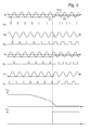
- Figure 3 shows a temporal diagram of the different signals through the automatic gain control unit for defining the detection of a high amplitude level of alternative intermediate signals Ip, Qp, In, Qn and for attenuating the gain of an amplifier of the receiver.
- the stored voltage V CC on the storage capacitor begins at a high level for example at 1.8 V, whereas the output signal V ST of the bi-stable trigger element is at a low level for example at 0 V.
- the amplitude level of the four alternative intermediate signals Ip, Qp, In, Qn is shown too high and lower than the first reference threshold th1 on the lower side.
- the first reference threshold th1 can be for example at 0.72 V.
- the peak to peak voltage level of the alternative intermediate signals Ip, Qp, In, Qn can be for example slightly less than 200 mV centred on the common mode voltage V cm at 0.8 V.
- each NMOS transistor is conductive during the width of the respective pulse of the control signal S C1 , S C2 , S C3 , S C4 .
- the second current I2 multiplied by ⁇ T/T becomes greater than the first current value I1. So the voltage level V CC on the storage capacitor progressively decreases from the high level at 1.8 V to a low level at 0 V, that can be programmable to set the AGC attack time.
- the output voltage V ST from the bi-stable trigger element commutes from the low voltage level to a high voltage level at 1.8 V to attenuate the gain of the amplifier by 12 dB.
- the commutation from the low level to the high level at the output of the bi-stable trigger element controls the multiplexer of the selecting means in order to provide the second reference threshold th2 after the first reference threshold th1. So said second reference threshold th2 will be maintained until the amplitude level of the alternative intermediate signals drops under the second reference threshold th2, which can be approximately at 0.79 V, which defines the hysteresis by 3.5 dB to prevent chatter.
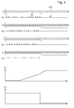
- Figure 4 shows a temporal diagram of signals through the automatic gain control unit for defining the detection of a low amplitude level of alternative intermediate signals Ip, Qp, In, Qn and in order to not attenuate the gain of an amplifier of the receiver.
- the stored voltage V CC on the storage capacitor begins at a low level for example at 0 V, whereas the output signal V ST of the bi-stable trigger element is at a high level for example at 1.8 V for attenuating the gain of the amplifier.
- the amplitude level of the four alternative intermediate signals Ip, Qp, In, Qn is shown too low and approximately at the level of the second reference threshold th2 selected on the lower side.
- the second reference threshold th2 can be for example at 0.79 V.
- the peak to peak voltage level of the alternative intermediate signals Ip, Qp, In, Qn can be for example at 20 mv or slightly less than 20 mV centred on the common mode voltage V cm at 0.8 V.
- each NMOS transistor is conductive during a small width of the respective pulse of the control signal S C1 , S C2 , S C3 , S C4 .
- the second current I2 multiplied by ⁇ T/T becomes smaller than the first current value I1. So the voltage level V CC on the storage capacitor progressively increases from the low level at 0 V to a high level at 1.8 V, that can be programmable to set the AGC decay time.
- the output voltage V ST from the bi-stable trigger element commutes from the high voltage level at 1.8 V to a low voltage level at 0 V to not attenuate the gain of the amplifier.
- the commutation from the high level to the low level at the output of the bi-stable trigger element controls the multiplexer of the selecting means in order to provide the first reference threshold th1 after the second reference threshold th2. So said first reference threshold th1 will be maintained until the amplitude level of the alternative intermediate signals increases to be under the first reference threshold th1, which can be approximately at 0.72 V.
- the automatic gain control unit can be also conceived with only one comparator 11 to compare a first alternative intermediate signal Ip with the first reference threshold th1 or the second reference threshold th2.
- the second current I2 multiplied by ⁇ T/T has to be greater than the first current I1 for controlling an attenuation of the amplifier.
- the automatic gain control unit can be also conceived with two comparators to compare an in-phase intermediate signal and a quarter-phase intermediate signal with the first reference threshold th1 or the second reference threshold th2.
- the first reference threshold th1 or the second reference threshold th2 from the selecting means can be defined for a comparison on an upper side of one alternative intermediate signal or two alternative intermediate signals, or the four alternative intermediate signals Ip, In, Qp, Qn.
- the resistor divider can be connected between the output of the voltage follower and the high potential terminal of the supply voltage source.
- the first reference threshold th1 or the second reference threshold th2 are connected at negative input of each comparator, whereas each alternative intermediate signal is connected at positive input of each comparator, if a NMOS transistor is always used at output of each comparator.
- comparators are used to compare the alternative intermediate signals with the first reference threshold or the second reference threshold on the lower side or the upper side, it can be envisaged to connect a PMOS transistor at output of each comparator. However the first reference threshold or the second reference threshold are received at negative input of each comparator for a comparison on the lower side and at positive input of each comparator for a comparison on the upper side inversely from the case with a NMOS transistor.
- the second current source at the high potential terminal of the supply voltage source, whereas the first current source can be connected at the low potential terminal of the supply voltage source.
- the second current can charge the storage capacitor, whereas the first current is used to discharge said storage capacitor.
- the AGC output signal can be directly supplied at the output of the bi-stable trigger element.
Landscapes
- Engineering & Computer Science (AREA)
- Computer Networks & Wireless Communication (AREA)
- Signal Processing (AREA)
- Circuits Of Receivers In General (AREA)
- Control Of Amplification And Gain Control (AREA)
Applications Claiming Priority (1)
| Application Number | Priority Date | Filing Date | Title |
|---|---|---|---|
| US13/716,657 US8848770B2 (en) | 2012-12-17 | 2012-12-17 | Automatic gain control unit for a low power receiver or transceiver |
Publications (3)
| Publication Number | Publication Date |
|---|---|
| EP2744104A2 true EP2744104A2 (de) | 2014-06-18 |
| EP2744104A3 EP2744104A3 (de) | 2015-09-30 |
| EP2744104B1 EP2744104B1 (de) | 2016-08-24 |
Family
ID=49554145
Family Applications (1)
| Application Number | Title | Priority Date | Filing Date |
|---|---|---|---|
| EP13192529.9A Active EP2744104B1 (de) | 2012-12-17 | 2013-11-12 | Automatische Verstärkungs-Steuerungseinheit für einen Empfänger oder -Sender-Empfänger mit geringer Leistungsaufnahme |
Country Status (2)
| Country | Link |
|---|---|
| US (1) | US8848770B2 (de) |
| EP (1) | EP2744104B1 (de) |
Families Citing this family (4)
| Publication number | Priority date | Publication date | Assignee | Title |
|---|---|---|---|---|
| US9264084B2 (en) * | 2013-05-30 | 2016-02-16 | Silicon Laboratories Inc. | Radio receiver having enhanced automatic gain control circuitry |
| US8983402B2 (en) * | 2013-08-13 | 2015-03-17 | National Sun Yat-Sen University | Transceiver with wake up detection |
| US10771293B2 (en) * | 2018-12-07 | 2020-09-08 | Commscope Technologies Llc | Systems and methods for automatic level control |
| WO2021004600A1 (en) * | 2019-07-05 | 2021-01-14 | Telefonaktiebolaget Lm Ericsson (Publ) | Wireless device |
Family Cites Families (5)
| Publication number | Priority date | Publication date | Assignee | Title |
|---|---|---|---|---|
| US5600681A (en) * | 1993-03-05 | 1997-02-04 | Max B. Gut | Method and equipment for the reception of digital signals |
| US6418303B1 (en) * | 2000-02-29 | 2002-07-09 | Motorola, Inc. | Fast attack automatic gain control (AGC) loop and methodology for narrow band receivers |
| US20070237273A1 (en) * | 2006-03-02 | 2007-10-11 | Seeteck Tan | Complex filter with automatic tuning capabilities |
| KR100835983B1 (ko) * | 2006-12-05 | 2008-06-09 | 한국전자통신연구원 | 자동 이득 조절을 위한 검출기 |
| JP5491969B2 (ja) * | 2010-05-31 | 2014-05-14 | ローム株式会社 | トランスミッタ、インタフェイス装置、車載通信システム |
-
2012
- 2012-12-17 US US13/716,657 patent/US8848770B2/en active Active
-
2013
- 2013-11-12 EP EP13192529.9A patent/EP2744104B1/de active Active
Non-Patent Citations (1)
| Title |
|---|
| None |
Also Published As
| Publication number | Publication date |
|---|---|
| US8848770B2 (en) | 2014-09-30 |
| US20140169417A1 (en) | 2014-06-19 |
| EP2744104A3 (de) | 2015-09-30 |
| EP2744104B1 (de) | 2016-08-24 |
Similar Documents
| Publication | Publication Date | Title |
|---|---|---|
| US7761072B2 (en) | GPS receiver with improved immunity to burst transmissions | |
| US7005922B2 (en) | Variable gain amplifier circuit and gain control method thereof | |
| US7589657B2 (en) | Analog to digital converter with interference rejection capability | |
| US20080252367A1 (en) | Demodulator with Multiple Operating Modes for Amplitude Shift Keyed Signals | |
| EP2744104B1 (de) | Automatische Verstärkungs-Steuerungseinheit für einen Empfänger oder -Sender-Empfänger mit geringer Leistungsaufnahme | |
| US7692486B2 (en) | Configurable feedback for an amplifier | |
| KR910009665B1 (ko) | 무선 수신기의 전원 절약회로 및 그 제어방법 | |
| CN107919859B (zh) | 基于过载状况的持续时间来控制放大器增益的自动增益控制(agc)电路和方法 | |
| EP2555424B1 (de) | Automatischer schrittvariabler Abschwächer und Funkkommunikationsvorrichtung | |
| KR100956667B1 (ko) | 트랜스시버 디바이스에 대한 디지털 자동 이득 제어 | |
| US11658764B2 (en) | Biasing technique for receiver based on radio frequency (RF) jammer detection | |
| Moody et al. | A highly reconfigurable bit-level duty-cycled TRF receiver achieving− 106-dBm sensitivity and 33-nW average power consumption | |
| EP1959575A2 (de) | FM-Empfänger | |
| US20230032217A1 (en) | Preamble Signal for Wakeup Communication in a Wireless Communication System | |
| EP1504527B1 (de) | Digitale automatische verstärkungsregelung für sender-empfängervorrichtungen | |
| US7373125B2 (en) | Off-channel signal detector with programmable hysteresis | |
| US20040017861A1 (en) | Slice circuit capable of accurate conversion of an analog signal to a digital signal | |
| EP1071202A2 (de) | PLL-Amplitudendemodulator | |
| US20100220817A1 (en) | Data Slicer with Multi-Mode Threshold Generator | |
| JP5074279B2 (ja) | 信号処理装置 | |
| US7894558B2 (en) | Receiving circuit for multi-slot receiving provided with circuit for adjusting frequency characteristic of active filter | |
| US9722648B2 (en) | Integrated circuit device, electronic device and method for frequency detection | |
| US8838055B2 (en) | Dynamic sub-sampling radio frequency mixer systems and methods | |
| JP4873387B2 (ja) | 利得制御方法 | |
| US20110034143A1 (en) | Method and circuit for a fast reduction in voltage of a dc component and low-frequency components at a mixing circuit output in a receiver of a uhf transceiver |
Legal Events
| Date | Code | Title | Description |
|---|---|---|---|
| PUAI | Public reference made under article 153(3) epc to a published international application that has entered the european phase |
Free format text: ORIGINAL CODE: 0009012 |
|
| 17P | Request for examination filed |
Effective date: 20131112 |
|
| AK | Designated contracting states |
Kind code of ref document: A2 Designated state(s): AL AT BE BG CH CY CZ DE DK EE ES FI FR GB GR HR HU IE IS IT LI LT LU LV MC MK MT NL NO PL PT RO RS SE SI SK SM TR |
|
| AX | Request for extension of the european patent |
Extension state: BA ME |
|
| PUAL | Search report despatched |
Free format text: ORIGINAL CODE: 0009013 |
|
| AK | Designated contracting states |
Kind code of ref document: A3 Designated state(s): AL AT BE BG CH CY CZ DE DK EE ES FI FR GB GR HR HU IE IS IT LI LT LU LV MC MK MT NL NO PL PT RO RS SE SI SK SM TR |
|
| AX | Request for extension of the european patent |
Extension state: BA ME |
|
| RIC1 | Information provided on ipc code assigned before grant |
Ipc: H03G 3/30 20060101AFI20150827BHEP |
|
| GRAP | Despatch of communication of intention to grant a patent |
Free format text: ORIGINAL CODE: EPIDOSNIGR1 |
|
| R17P | Request for examination filed (corrected) |
Effective date: 20160330 |
|
| RBV | Designated contracting states (corrected) |
Designated state(s): AL AT BE BG CH CY CZ DE DK EE ES FI FR GB GR HR HU IE IS IT LI LT LU LV MC MK MT NL NO PL PT RO RS SE SI SK SM TR |
|
| INTG | Intention to grant announced |
Effective date: 20160512 |
|
| GRAS | Grant fee paid |
Free format text: ORIGINAL CODE: EPIDOSNIGR3 |
|
| GRAA | (expected) grant |
Free format text: ORIGINAL CODE: 0009210 |
|
| AK | Designated contracting states |
Kind code of ref document: B1 Designated state(s): AL AT BE BG CH CY CZ DE DK EE ES FI FR GB GR HR HU IE IS IT LI LT LU LV MC MK MT NL NO PL PT RO RS SE SI SK SM TR |
|
| REG | Reference to a national code |
Ref country code: GB Ref legal event code: FG4D |
|
| REG | Reference to a national code |
Ref country code: CH Ref legal event code: EP |
|
| REG | Reference to a national code |
Ref country code: AT Ref legal event code: REF Ref document number: 823866 Country of ref document: AT Kind code of ref document: T Effective date: 20160915 |
|
| REG | Reference to a national code |
Ref country code: IE Ref legal event code: FG4D |
|
| REG | Reference to a national code |
Ref country code: DE Ref legal event code: R096 Ref document number: 602013010564 Country of ref document: DE |
|
| REG | Reference to a national code |
Ref country code: CH Ref legal event code: NV Representative=s name: ICB INGENIEURS CONSEILS EN BREVETS SA, CH |
|
| REG | Reference to a national code |
Ref country code: FR Ref legal event code: PLFP Year of fee payment: 4 |
|
| REG | Reference to a national code |
Ref country code: LT Ref legal event code: MG4D |
|
| REG | Reference to a national code |
Ref country code: NL Ref legal event code: MP Effective date: 20160824 |
|
| REG | Reference to a national code |
Ref country code: AT Ref legal event code: MK05 Ref document number: 823866 Country of ref document: AT Kind code of ref document: T Effective date: 20160824 |
|
| PG25 | Lapsed in a contracting state [announced via postgrant information from national office to epo] |
Ref country code: FI Free format text: LAPSE BECAUSE OF FAILURE TO SUBMIT A TRANSLATION OF THE DESCRIPTION OR TO PAY THE FEE WITHIN THE PRESCRIBED TIME-LIMIT Effective date: 20160824 Ref country code: RS Free format text: LAPSE BECAUSE OF FAILURE TO SUBMIT A TRANSLATION OF THE DESCRIPTION OR TO PAY THE FEE WITHIN THE PRESCRIBED TIME-LIMIT Effective date: 20160824 Ref country code: IT Free format text: LAPSE BECAUSE OF FAILURE TO SUBMIT A TRANSLATION OF THE DESCRIPTION OR TO PAY THE FEE WITHIN THE PRESCRIBED TIME-LIMIT Effective date: 20160824 Ref country code: NO Free format text: LAPSE BECAUSE OF FAILURE TO SUBMIT A TRANSLATION OF THE DESCRIPTION OR TO PAY THE FEE WITHIN THE PRESCRIBED TIME-LIMIT Effective date: 20161124 Ref country code: NL Free format text: LAPSE BECAUSE OF FAILURE TO SUBMIT A TRANSLATION OF THE DESCRIPTION OR TO PAY THE FEE WITHIN THE PRESCRIBED TIME-LIMIT Effective date: 20160824 Ref country code: LT Free format text: LAPSE BECAUSE OF FAILURE TO SUBMIT A TRANSLATION OF THE DESCRIPTION OR TO PAY THE FEE WITHIN THE PRESCRIBED TIME-LIMIT Effective date: 20160824 Ref country code: HR Free format text: LAPSE BECAUSE OF FAILURE TO SUBMIT A TRANSLATION OF THE DESCRIPTION OR TO PAY THE FEE WITHIN THE PRESCRIBED TIME-LIMIT Effective date: 20160824 |
|
| PG25 | Lapsed in a contracting state [announced via postgrant information from national office to epo] |
Ref country code: GR Free format text: LAPSE BECAUSE OF FAILURE TO SUBMIT A TRANSLATION OF THE DESCRIPTION OR TO PAY THE FEE WITHIN THE PRESCRIBED TIME-LIMIT Effective date: 20161125 Ref country code: BE Free format text: LAPSE BECAUSE OF NON-PAYMENT OF DUE FEES Effective date: 20161130 Ref country code: AT Free format text: LAPSE BECAUSE OF FAILURE TO SUBMIT A TRANSLATION OF THE DESCRIPTION OR TO PAY THE FEE WITHIN THE PRESCRIBED TIME-LIMIT Effective date: 20160824 Ref country code: ES Free format text: LAPSE BECAUSE OF FAILURE TO SUBMIT A TRANSLATION OF THE DESCRIPTION OR TO PAY THE FEE WITHIN THE PRESCRIBED TIME-LIMIT Effective date: 20160824 Ref country code: PT Free format text: LAPSE BECAUSE OF FAILURE TO SUBMIT A TRANSLATION OF THE DESCRIPTION OR TO PAY THE FEE WITHIN THE PRESCRIBED TIME-LIMIT Effective date: 20161226 Ref country code: SE Free format text: LAPSE BECAUSE OF FAILURE TO SUBMIT A TRANSLATION OF THE DESCRIPTION OR TO PAY THE FEE WITHIN THE PRESCRIBED TIME-LIMIT Effective date: 20160824 Ref country code: LV Free format text: LAPSE BECAUSE OF FAILURE TO SUBMIT A TRANSLATION OF THE DESCRIPTION OR TO PAY THE FEE WITHIN THE PRESCRIBED TIME-LIMIT Effective date: 20160824 |
|
| PG25 | Lapsed in a contracting state [announced via postgrant information from national office to epo] |
Ref country code: EE Free format text: LAPSE BECAUSE OF FAILURE TO SUBMIT A TRANSLATION OF THE DESCRIPTION OR TO PAY THE FEE WITHIN THE PRESCRIBED TIME-LIMIT Effective date: 20160824 Ref country code: RO Free format text: LAPSE BECAUSE OF FAILURE TO SUBMIT A TRANSLATION OF THE DESCRIPTION OR TO PAY THE FEE WITHIN THE PRESCRIBED TIME-LIMIT Effective date: 20160824 |
|
| REG | Reference to a national code |
Ref country code: DE Ref legal event code: R097 Ref document number: 602013010564 Country of ref document: DE |
|
| PG25 | Lapsed in a contracting state [announced via postgrant information from national office to epo] |
Ref country code: BG Free format text: LAPSE BECAUSE OF FAILURE TO SUBMIT A TRANSLATION OF THE DESCRIPTION OR TO PAY THE FEE WITHIN THE PRESCRIBED TIME-LIMIT Effective date: 20161124 Ref country code: SM Free format text: LAPSE BECAUSE OF FAILURE TO SUBMIT A TRANSLATION OF THE DESCRIPTION OR TO PAY THE FEE WITHIN THE PRESCRIBED TIME-LIMIT Effective date: 20160824 Ref country code: SK Free format text: LAPSE BECAUSE OF FAILURE TO SUBMIT A TRANSLATION OF THE DESCRIPTION OR TO PAY THE FEE WITHIN THE PRESCRIBED TIME-LIMIT Effective date: 20160824 Ref country code: DK Free format text: LAPSE BECAUSE OF FAILURE TO SUBMIT A TRANSLATION OF THE DESCRIPTION OR TO PAY THE FEE WITHIN THE PRESCRIBED TIME-LIMIT Effective date: 20160824 Ref country code: CZ Free format text: LAPSE BECAUSE OF FAILURE TO SUBMIT A TRANSLATION OF THE DESCRIPTION OR TO PAY THE FEE WITHIN THE PRESCRIBED TIME-LIMIT Effective date: 20160824 Ref country code: BE Free format text: LAPSE BECAUSE OF FAILURE TO SUBMIT A TRANSLATION OF THE DESCRIPTION OR TO PAY THE FEE WITHIN THE PRESCRIBED TIME-LIMIT Effective date: 20160824 Ref country code: PL Free format text: LAPSE BECAUSE OF FAILURE TO SUBMIT A TRANSLATION OF THE DESCRIPTION OR TO PAY THE FEE WITHIN THE PRESCRIBED TIME-LIMIT Effective date: 20160824 |
|
| PLBE | No opposition filed within time limit |
Free format text: ORIGINAL CODE: 0009261 |
|
| STAA | Information on the status of an ep patent application or granted ep patent |
Free format text: STATUS: NO OPPOSITION FILED WITHIN TIME LIMIT |
|
| 26N | No opposition filed |
Effective date: 20170526 |
|
| REG | Reference to a national code |
Ref country code: IE Ref legal event code: MM4A |
|
| PG25 | Lapsed in a contracting state [announced via postgrant information from national office to epo] |
Ref country code: SI Free format text: LAPSE BECAUSE OF FAILURE TO SUBMIT A TRANSLATION OF THE DESCRIPTION OR TO PAY THE FEE WITHIN THE PRESCRIBED TIME-LIMIT Effective date: 20160824 |
|
| PG25 | Lapsed in a contracting state [announced via postgrant information from national office to epo] |
Ref country code: LU Free format text: LAPSE BECAUSE OF NON-PAYMENT OF DUE FEES Effective date: 20161130 |
|
| REG | Reference to a national code |
Ref country code: FR Ref legal event code: PLFP Year of fee payment: 5 |
|
| PG25 | Lapsed in a contracting state [announced via postgrant information from national office to epo] |
Ref country code: IE Free format text: LAPSE BECAUSE OF NON-PAYMENT OF DUE FEES Effective date: 20161112 |
|
| PG25 | Lapsed in a contracting state [announced via postgrant information from national office to epo] |
Ref country code: HU Free format text: LAPSE BECAUSE OF FAILURE TO SUBMIT A TRANSLATION OF THE DESCRIPTION OR TO PAY THE FEE WITHIN THE PRESCRIBED TIME-LIMIT; INVALID AB INITIO Effective date: 20131112 |
|
| PG25 | Lapsed in a contracting state [announced via postgrant information from national office to epo] |
Ref country code: MK Free format text: LAPSE BECAUSE OF FAILURE TO SUBMIT A TRANSLATION OF THE DESCRIPTION OR TO PAY THE FEE WITHIN THE PRESCRIBED TIME-LIMIT Effective date: 20160824 Ref country code: MC Free format text: LAPSE BECAUSE OF FAILURE TO SUBMIT A TRANSLATION OF THE DESCRIPTION OR TO PAY THE FEE WITHIN THE PRESCRIBED TIME-LIMIT Effective date: 20160824 Ref country code: CY Free format text: LAPSE BECAUSE OF FAILURE TO SUBMIT A TRANSLATION OF THE DESCRIPTION OR TO PAY THE FEE WITHIN THE PRESCRIBED TIME-LIMIT Effective date: 20160824 Ref country code: IS Free format text: LAPSE BECAUSE OF FAILURE TO SUBMIT A TRANSLATION OF THE DESCRIPTION OR TO PAY THE FEE WITHIN THE PRESCRIBED TIME-LIMIT Effective date: 20160824 |
|
| GBPC | Gb: european patent ceased through non-payment of renewal fee |
Effective date: 20171112 |
|
| PG25 | Lapsed in a contracting state [announced via postgrant information from national office to epo] |
Ref country code: MT Free format text: LAPSE BECAUSE OF NON-PAYMENT OF DUE FEES Effective date: 20161112 |
|
| REG | Reference to a national code |
Ref country code: FR Ref legal event code: PLFP Year of fee payment: 6 |
|
| PG25 | Lapsed in a contracting state [announced via postgrant information from national office to epo] |
Ref country code: TR Free format text: LAPSE BECAUSE OF FAILURE TO SUBMIT A TRANSLATION OF THE DESCRIPTION OR TO PAY THE FEE WITHIN THE PRESCRIBED TIME-LIMIT Effective date: 20160824 Ref country code: AL Free format text: LAPSE BECAUSE OF FAILURE TO SUBMIT A TRANSLATION OF THE DESCRIPTION OR TO PAY THE FEE WITHIN THE PRESCRIBED TIME-LIMIT Effective date: 20160824 |
|
| PG25 | Lapsed in a contracting state [announced via postgrant information from national office to epo] |
Ref country code: GB Free format text: LAPSE BECAUSE OF NON-PAYMENT OF DUE FEES Effective date: 20171112 |
|
| P01 | Opt-out of the competence of the unified patent court (upc) registered |
Effective date: 20230611 |
|
| REG | Reference to a national code |
Ref country code: CH Ref legal event code: U11 Free format text: ST27 STATUS EVENT CODE: U-0-0-U10-U11 (AS PROVIDED BY THE NATIONAL OFFICE) Effective date: 20251201 |
|
| PGFP | Annual fee paid to national office [announced via postgrant information from national office to epo] |
Ref country code: DE Payment date: 20251022 Year of fee payment: 13 |
|
| PGFP | Annual fee paid to national office [announced via postgrant information from national office to epo] |
Ref country code: FR Payment date: 20251022 Year of fee payment: 13 |
|
| PGFP | Annual fee paid to national office [announced via postgrant information from national office to epo] |
Ref country code: CH Payment date: 20251201 Year of fee payment: 13 |