EP2745400B1 - Avalanche-impulsgeber - Google Patents
Avalanche-impulsgeber Download PDFInfo
- Publication number
- EP2745400B1 EP2745400B1 EP12758938.0A EP12758938A EP2745400B1 EP 2745400 B1 EP2745400 B1 EP 2745400B1 EP 12758938 A EP12758938 A EP 12758938A EP 2745400 B1 EP2745400 B1 EP 2745400B1
- Authority
- EP
- European Patent Office
- Prior art keywords
- pulse
- transistor
- voltage
- input signal
- terminal
- Prior art date
- Legal status (The legal status is an assumption and is not a legal conclusion. Google has not performed a legal analysis and makes no representation as to the accuracy of the status listed.)
- Not-in-force
Links
- 238000000034 method Methods 0.000 claims description 23
- 239000003990 capacitor Substances 0.000 claims description 14
- 230000004044 response Effects 0.000 claims description 14
- 230000008878 coupling Effects 0.000 claims description 4
- 238000010168 coupling process Methods 0.000 claims description 4
- 238000005859 coupling reaction Methods 0.000 claims description 4
- 230000008569 process Effects 0.000 claims description 4
- 238000011084 recovery Methods 0.000 claims description 3
- 238000013016 damping Methods 0.000 claims description 2
- 230000008901 benefit Effects 0.000 description 4
- 230000008859 change Effects 0.000 description 4
- 230000000630 rising effect Effects 0.000 description 4
- 230000000149 penetrating effect Effects 0.000 description 2
- 230000005855 radiation Effects 0.000 description 2
- 230000001960 triggered effect Effects 0.000 description 2
- 230000005284 excitation Effects 0.000 description 1
- 230000001939 inductive effect Effects 0.000 description 1
- 230000007704 transition Effects 0.000 description 1
Images


Classifications
-
- H—ELECTRICITY
- H03—ELECTRONIC CIRCUITRY
- H03K—PULSE TECHNIQUE
- H03K3/00—Circuits for generating electric pulses; Monostable, bistable or multistable circuits
- H03K3/02—Generators characterised by the type of circuit or by the means used for producing pulses
- H03K3/335—Generators characterised by the type of circuit or by the means used for producing pulses by the use, as active elements, of semiconductor devices with more than two electrodes and exhibiting avalanche effect
-
- G—PHYSICS
- G01—MEASURING; TESTING
- G01S—RADIO DIRECTION-FINDING; RADIO NAVIGATION; DETERMINING DISTANCE OR VELOCITY BY USE OF RADIO WAVES; LOCATING OR PRESENCE-DETECTING BY USE OF THE REFLECTION OR RERADIATION OF RADIO WAVES; ANALOGOUS ARRANGEMENTS USING OTHER WAVES
- G01S13/00—Systems using the reflection or reradiation of radio waves, e.g. radar systems; Analogous systems using reflection or reradiation of waves whose nature or wavelength is irrelevant or unspecified
- G01S13/02—Systems using reflection of radio waves, e.g. primary radar systems; Analogous systems
- G01S13/06—Systems determining position data of a target
- G01S13/08—Systems for measuring distance only
- G01S13/10—Systems for measuring distance only using transmission of interrupted, pulse modulated waves
- G01S13/14—Systems for measuring distance only using transmission of interrupted, pulse modulated waves wherein a voltage or current pulse is initiated and terminated in accordance respectively with the pulse transmission and echo reception
-
- G—PHYSICS
- G01—MEASURING; TESTING
- G01S—RADIO DIRECTION-FINDING; RADIO NAVIGATION; DETERMINING DISTANCE OR VELOCITY BY USE OF RADIO WAVES; LOCATING OR PRESENCE-DETECTING BY USE OF THE REFLECTION OR RERADIATION OF RADIO WAVES; ANALOGOUS ARRANGEMENTS USING OTHER WAVES
- G01S13/00—Systems using the reflection or reradiation of radio waves, e.g. radar systems; Analogous systems using reflection or reradiation of waves whose nature or wavelength is irrelevant or unspecified
- G01S13/88—Radar or analogous systems specially adapted for specific applications
- G01S13/885—Radar or analogous systems specially adapted for specific applications for ground probing
-
- G—PHYSICS
- G01—MEASURING; TESTING
- G01S—RADIO DIRECTION-FINDING; RADIO NAVIGATION; DETERMINING DISTANCE OR VELOCITY BY USE OF RADIO WAVES; LOCATING OR PRESENCE-DETECTING BY USE OF THE REFLECTION OR RERADIATION OF RADIO WAVES; ANALOGOUS ARRANGEMENTS USING OTHER WAVES
- G01S7/00—Details of systems according to groups G01S13/00, G01S15/00, G01S17/00
- G01S7/02—Details of systems according to groups G01S13/00, G01S15/00, G01S17/00 of systems according to group G01S13/00
- G01S7/03—Details of HF subsystems specially adapted therefor, e.g. common to transmitter and receiver
- G01S7/032—Constructional details for solid-state radar subsystems
-
- G—PHYSICS
- G01—MEASURING; TESTING
- G01S—RADIO DIRECTION-FINDING; RADIO NAVIGATION; DETERMINING DISTANCE OR VELOCITY BY USE OF RADIO WAVES; LOCATING OR PRESENCE-DETECTING BY USE OF THE REFLECTION OR RERADIATION OF RADIO WAVES; ANALOGOUS ARRANGEMENTS USING OTHER WAVES
- G01S7/00—Details of systems according to groups G01S13/00, G01S15/00, G01S17/00
- G01S7/02—Details of systems according to groups G01S13/00, G01S15/00, G01S17/00 of systems according to group G01S13/00
- G01S7/28—Details of pulse systems
- G01S7/282—Transmitters
Definitions
- This disclosure relates to systems and methods for generating a pulse. Consistent with this disclosure, the generated pulses can be used in radar applications.
- An example for a radar system can be found in document WO 2009/038898 .
- the present disclosure is directed to a circuit for generating a pulse as defined in claim 1.
- the circuit includes a transistor and a pulse generating circuit.
- the transistor is constructed and arranged to be operable in an avalanche mode.
- the pulse generating circuit is constructed and arranged to: receive at least one trigger input signal; generate a voltage pulse having a duration less than an avalanche time of the transistor in response to at least a portion of the at least one trigger input signal; and transmit the voltage pulse to a terminal of the transistor.
- the transistor is constructed and arranged to output an avalanche pulse from at least one terminal of the transistor in response to the voltage pulse with a negative bias generator and a SRD diode.
- the present disclosure is directed to a method for generating a pulse.
- the method includes receiving at least one trigger input signal with a pulse generating circuit and generating, with the pulse generating circuit, a voltage pulse in response to at least a portion of the at least one trigger input signal.
- the method also includes transmitting the voltage pulse from the pulse generating circuit to a terminal of a transistor constructed and arranged to be operable in an avalanche mode, and outputting an avalanche pulse from at least one terminal of the transistor in response to the voltage pulse.
- the voltage pulse has a duration less than an avalanche time of the transistor.
- the method further includes generating a negative voltage with a negative bias generator and using a SRD diode as defined in claim 7.
- the present disclosure is directed to a radar system as defined in claim 13.
- the radar system includes a circuit including a transistor and a pulse generating circuit.
- the transistor is constructed and arranged to be operable in an avalanche mode.
- the pulse generating circuit is constructed and arranged to: receive at least one trigger input signal; generate a voltage pulse having a duration less than an avalanche time of the transistor in response to at least a portion of the at least one trigger input signal; and transmit the voltage pulse to a terminal of the transistor.
- the transistor is constructed and arranged to output an avalanche pulse from at least one terminal of the transistor in response to the voltage pulse.
- the radar system further includes an antenna connected to the circuit, where the antenna is constructed and arranged to transmit the avalanche pulse and receive a return pulse.
- the radar system further includes a processor connected to the antenna, where the processor is constructed and arranged to process the return pulse, generate image data, and transmit the image data to a display.
- the present disclosure is directed to a method for creating a radar image as defined in claim 15.
- the method includes receiving: at least one trigger input signal with a pulse generating circuit; generating, with the pulse generating circuit, a voltage pulse in response to at least a portion of the at least one trigger input signal; and transmitting the voltage pulse from the pulse generating circuit to a terminal of a transistor constructed and arranged to be operable in an avalanche mode.
- the method also includes outputting an avalanche pulse from at least one terminal of the transistor to an antenna in response to the voltage pulse, transmitting the avalanche pulse with the antenna, receiving a return pulse with the antenna, processing the return pulse with a processor to generate image data, and transmitting the image data to a display.
- the voltage pulse has a duration less than an avalanche time of the transistor.
- GPR ground penetrating radar
- a GPR system consistent with this disclosure can be configured to transmit narrow pulses of high energy into the ground to detect buried objects.
- FIG. 1 An embodiment of a GPR system consistent with this disclosure is depicted in FIG. 1 .
- the GPR system can include transmitter unit 10, a receiver unit 70, a processing unit 20, a display unit 30, a control unit 40, and/or other components.
- a transmitter/receiver unit consistent with this disclosure can include one or more elements 15 and 75 (e.g. antennas) that transmit radar signals and receive returned signals.
- Transmitter and receiver elements 15 and 75 can be separate (as depicted) or can be integrated into a single element (i.e., a transceiver element).
- Embodiments of circuits consistent with this disclosure can be used to generate transmit pulses which can be delivered to the transmitter element(s) 15.
- the transmitter element(s) 15 can radiate the pulses. These radiated pulses can travel into the ground 60, and a buried object 65 can reflect the radiated pulses. Reflected radiation received by the receiver element(s) 75 can enable the GPR system to provide data about buried objects to a user.
- the processing unit 20 can process the received radiation to form image data and transmit the image data to the display unit 30 which can allow a user to view the buried object data.
- the control unit 40 can be provided to control the operation of: a pulse generating circuit consistent with this disclosure (for example by providing or controlling an input signal), the processing unit 20, and/or the display unit 30.
- control and processing operations can be performed by one or more processors and/or by one or more circuits.
- control and processing functions can be performed by the same one or more processors and/or circuits.
- Avalanche transistors can be used to generate the pulses used by GPR systems consistent with this disclosure, and in other applications.
- Avalanche pulses can themselves be triggered by trigger pulses. For example, the rising edge of a trigger pulse can cause the avalanche pulse in some transistors. If the trigger pulse remains high for a time longer than a length of the avalanche pulse, the avalanche transistor can enter an "on" state and emit noise.
- a brief trigger pulse with a fast rising and falling edge can trigger an avalanche pulse with little or no noise.
- FIG. 2 depicts an avalanche pulser circuit 100 according to an embodiment consistent with this disclosure.
- Embodiments of the avalanche pulser circuit 100 can include a transistor 101 which can operate in avalanche mode.
- the transistor 101 can be an NPN transistor or any other transistor capable of operating in avalanche mode.
- current can flow from a high voltage source 110 through the transistor 101.
- the high voltage from the high voltage source 110 can be stored on a capacitor or capacitors 115, or the high voltage can flow from the high voltage source 110 through a resistor 111.
- the capacitor 115 can be present between the collector 102 and ground to facilitate avalanche operation in the transistor 101.
- a capacitor or capacitors 112 can be present between the high voltage source 110 and ground and can filter noise in the high voltage source 110.
- the high voltage source 110 can be set to a voltage that can allow triggerable avalanche in the transistor 101.
- an output 160 such as a 50 ohm output 160, can be taken at the emitter 104.
- a resistance, such as the 50 ohm resistor 153 shown in this example, can also be provided between the emitter 104 and ground to create the 50 ohm output.
- the avalanche pulser circuit 100 can comprise a pulse generating circuit 130 which can feed a triggering signal to a base 103 of the transistor 101.
- a trigger input 120 can be fed into the pulse generating circuit 130.
- the pulse generating circuit 130 can comprise a step recovery diode 131 (SRD) and inductor 132.
- the pulse generating circuit 130 can also comprise a damping resistor 133 at the SRD 131 cathode and a capacitor 135 and resistor 134 at the SRD 131 anode.
- the SRD 131 and inductor 132 can be referenced to a negative voltage by a negative bias 140.
- a capacitor or capacitors 141 can be present between the negative bias 140 and ground and can stabilize the negative bias 140.
- Resistors 151, 152 can form a voltage divider at the base 103 in some embodiments.
- the impedance at the input to the base 103 can be made low (for example, 51.1 ohms) in some embodiments.
- the avalanche pulser circuit 100 can trigger avalanche in the transistor 101 with a pulse and bias the transistor 101 off before an avalanche-transmitted pulse is over.
- the transistor 101 can output a short pulse with fast rising and falling edges.
- FIG. 3 depicts a pulse which can be obtained in single-ended mode at the emitter 104 of the transistor 101. This example is a 15 V pulse.
- Such a pulse can have a rise time in the 85-150 picosecond range and a fall time in the 85-200 picosecond range. These rise and fall times can depend in part on the transistor 101 used.
- Some embodiments of the avalanche pulser circuit 100 can produce a pulse having a total width in the 250-350 picosecond range, for example.
- the output of the transistor 101 can be taken in differential output mode at the collector 102 and emitter 104.
- a 50 ohm resistor can be added in series with the collector capacitor 115.
- a collector 102 charge and discharge can be superimposed onto the differential output, but the transistor 101 can still be quickly biased off.
- a pulse generating circuit can be designed to provide a very short excitation pulse to the transistor 101.
- the trigger input 120 can be used to drive the pulse generating circuit 130 to produce a triggering signal at the base 103.
- the trigger input 120 can be a clock signal such as a square wave with a 50% duty cycle. Other embodiments can use other trigger inputs 120 having different waveforms and/or duty cycles.
- the trigger input 120 can oscillate between a positive maximum voltage and a negative minimum voltage.
- the pulse generating circuit 130 can receive the trigger input 120 and output a pulse trigger to the base 103.
- the negative voltage of the negative bias 140 can be selected so that when the trigger input 120 is at its maximum positive value, the SRD 131 can be conducting and the base 103 can be held to a negative voltage by the negative bias 140. During this period, the cathode of the SRD 131 can be at a negative voltage, and therefore the SRD 131 can be conducting in the anode to cathode direction and storing charge.
- the SRD 131 can behave according to the following equations.
- the SRD 131 can remain at a low impedance until the stored charge is depleted. Therefore, as long as t > 24 nanoseconds, the avalanche pulser circuit 100 can be independent of duty cycle.
- the base 103 can also be referenced below ground by the negative bias 140 during this period, which can prevent avalanche from occurring uncontrollably in the transistor 101.
- the negative edge of a trigger input signal can cause the SRD 131 to drain charge. When the charge is drained, the SRD 131 can rapidly switch to an off state and cause a rapid change in current. In response, the inductor 132 can produce a pulse that can trigger an avalanche in the transistor 101.
- An example of this process can proceed as follows. As noted above, in embodiments the trigger input 120 can transition from a positive voltage to a negative voltage. When the trigger input 120 is negative, the SRD 131 can conduct in the cathode to anode direction until all stored charge is swept away. When this happens, the SRD 131 can very rapidly stop conducting and cause a rapid change in current. The rapid current change can trigger a voltage pulse in the inductor 132.
- the pulse can rise quickly due to the rapid change in current and fall quickly due to the presence of the negative bias 140.
- a resistor or resistors 133 can be provided to damp the inductive pulse of the inductor 132. For example, with a 6 Vpp trigger input 120, a voltage pulse of approximately 2.5 V can be triggered in the inductor 132.
- the voltage pulse in the inductor 132 can be large enough to overcome the negative voltage at the base 103 of the transistor 101 to provide a positive voltage trigger at the base 103. This positive voltage can trigger avalanche in the transistor 101.
- the inductor 132 pulse can be a very brief pulse of less than one nanosecond, in some embodiments less than 300 picoseconds (e.g. 80-120 picoseconds).
- the pulse can be less than an avalanche time of the transistor 101, where the avalanche time is defined as a time elapsed from the triggering of the avalanche to its completion.
- This can be a sufficiently brief pulse such that positive voltage is no longer present at the base 103 when the avalanche completes, or the positive voltage can be removed from the base 103 concurrently with avalanche completion or shortly thereafter.
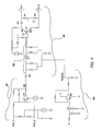
- FIG. 4 depicts an avalanche pulser circuit 300 according to a further embodiment of the invention.
- the avalanche pulser circuit 300 of FIG. 4 is similar to the avalanche pulser circuit 100 of FIG. 2 , but the output of the transistor 301 can be taken in differential output mode at the collector 302 and emitter 304 in the avalanche pulser circuit 300.
- 50 ohm output resistors 391 and 392 are added in series with the collector capacitor 315 and at the emitter 304.
- a differential output such as a 270 ohm differential, which can be chosen to match the impedence of an antenna, can be taken at the collector 302 and emitter 304.
- 270 ohm output resistors can be used in place of the 50 ohm output resistors 391 and 392.
- the operation of the avalanche pulser circuit 300 can be the same as the operation of the avalanche pulser circuit 100 of FIG. 2 , but with a differential output.
- the overall circuit depicted in FIG. 4 includes example trigger input generator 330 and negative bias generator 360 components.
- the trigger input generator 330 of FIG. 4 can include an amplifier 335.
- the amplifier 335 can shape the trigger pulse.
- the amplifier 335 can be an opamp or other amplifying circuit.
- An input signal can be supplied to the amplifier 335.
- the input signal can be a positive emitter coupled logic (PECL) level input signal with pulse repetition frequency of 16 MHz or less and a 50% duty cycle, though other signals and different frequencies can be used.
- PECL positive emitter coupled logic
- the amplifier 335 can amplify and/or condition the input signal.
- the amplifier 335 can output a 6 or 8 Vpp amplified square wave, though other outputs can be possible.
- a resistor or resistors 336 can limit the current out of the amplifier 335.
- the trigger input generator 330 can be AC coupled to the rest of the circuit 300 with an AC coupling capacitor 350.
- DC coupling can be used by omitting the capacitor 350 and setting the amplifier's 335 rails and summing a DC offset in order to drive the SRD 311.
- the negative bias generator 360 of FIG. 4 can include an amplifier 365.
- the amplifier 365 can receive a constant negative voltage or other signal and output a negative bias suitable for operation of the avalanche pulser circuit 300 as described above. For example, if the amplifier 335 is AC coupled and outputs a 6 Vpp signal, the negative bias generator 360 can output a -1 V signal so the input to the anode of the SRD 311 can be at or near zero volts when the amplifier 335 output is at or near its maximum voltage. This can prevent the transistor 301 from triggering on, as the cathode of the SRD 311 can be at a negative voltage below the voltage at the emitter 304 of the transistor 301.
- the negative bias generator 360 can employ an identical or substantially identical SRD 370 to the SRD 311 of the pulse trigger section 320 so that temperature compensation can be achieved.
- the example trigger input generator 330 and/or the example negative bias generator 360 of FIG. 4 can also be used with the avalanche pulser circuit 100 of FIG. 2 .
Landscapes
- Engineering & Computer Science (AREA)
- Radar, Positioning & Navigation (AREA)
- Remote Sensing (AREA)
- Physics & Mathematics (AREA)
- Computer Networks & Wireless Communication (AREA)
- General Physics & Mathematics (AREA)
- Electromagnetism (AREA)
- Radar Systems Or Details Thereof (AREA)
- Dc-Dc Converters (AREA)
Claims (15)
- Schaltung (100, 300) zum Erzeugen eines Pulses, umfassend:einen Transistor (101, 301), der so konstruiert und angeordnet ist, dass er in einem Lawinenmodus bedienbar ist; und eine pulserzeugende Schaltung (130), die so konstruiert und angeordnet ist, dass sie mindestens ein Triggereingangssignal empfängt,einen Spannungspuls mit einer Länge erzeugt, die kürzer ist als die Lawinendauer des Transistors (101, 301) in Reaktion auf zumindest einen Teil des mindestens einen Triggereingangssignals, und dass sie den Spannungspuls an einen Anschluss des Transistors (101, 301) überträgt;wobei der Transistor (101, 301) so konstruiert und angeordnet ist, dass er einen Lawinenpuls von mindestens einem Anschluss des Transistors (101, 301) in Reaktion auf den Spannungspuls ausgibt, dadurch gekennzeichnet, dass die Schaltung (100, 300) ferner umfasst: mindestens einen Generator für eine negative Vorspannung, der so konstruiert und angeordnet ist, dass er eine negative Spannung erzeugt;wobei die pulserzeugende Schaltung (130) umfasst:mindestens eine Speicherschaltdiode (SRD) (131, 311), welche auf die negative Spannung an einer Kathode der mindestens einen SRD (131, 311) referenziert ist, wobei die SRD (131, 311) so konstruiert und angeordnet ist, dass sie mindestens ein Triggereingangssignal an einer Anode der mindestens einen SRD (131, 311) empfängt,um Ladung zu speichern, wenn das mindestens eine Triggereingangssignal eine positive Spannung aufweist, und dass sie das Speichern der Ladung beendet, wenn das mindestens eine Triggereingangssignal eine negative Spannung aufweist; undmindestens einem Induktor (133), der so konstruiert und angeordnet ist, dass er den Spannungspuls erzeugt, nachdem die mindestens eine SRD (131, 311) das Speichern der Ladung beendet hat.
- Schaltung (100, 300) nach Anspruch 1, wobei der Transistor (101, 301) so konstruiert und angeordnet ist, dass er jederzeit in einem ausgeschalteten Zustand ist, außer zu einer Zeit, zu der der Spannungspuls an den Anschluss des Transistors (101, 301) übertragen wird, wobei die negative Spannung optional eine Spannung an einem Basisanschluss des Transistors (101, 301) verursacht, die jederzeit negativer ist als eine Spannung an einem Emitteranschluss des Transistors (101, 301), außer zu der Zeit, zu der der Spannungspuls an den Anschluss des Transmitters übertragen wird.
- Schaltung (100, 300) nach Anspruch 1, wobei der mindestens eine Generator einer negativen Vorspannung einen Verstärker (365) der negativen Vorspannung umfasst, der so konstruiert und angeordnet ist, dass er mindestens ein Eingangssignal negativer Vorspannung empfängt und zum Erzeugen der mindestens einen negativen Spannung das mindestens eine Eingangssignal negativer Vorspannung verstärkt, wobei der mindestens eine Generator negativer Vorspannung optional ferner mindestens eine temperaturkompensierte SRD (370) enthält, die im Wesentlichen mit der mindestens einen SRD (131, 311) identisch ist.
- Schaltung (100, 300) nach Anspruch 1, wobei die pulserzeugende Schaltung (130) ferner mindestens einen Widerstand umfasst, der so konstruiert und angeordnet ist, dass er den Spannungspuls drosselt; oder wobei der Transistor (101, 301) ein NPN-Transistor (101, 301) ist; oder wobei der Lawinenpuls eine Länge von etwa 250 bis 350 Picosekunden aufweist oder wobei der Spannungspuls eine Länge von weniger als 300 Picosekunden aufweist; oder wobei der Lawinenpuls an einem Emitteranschluss des Transistors (101, 301) ausgegeben wird, oder wobei der Lawinenpuls unterschiedlich an einem Kollektoranschluss und einem Emitteranschluss des Transistors (101, 301) ausgegeben wird.
- Schaltung (100, 300) nach Anspruch 1, ferner mindestens eine Spannungsquelle umfassend, die so konstruiert und angeordnet ist, dass sie mindestens ein Signal an einen Kollektoranschluss des Transistors (101, 301) überträgt; oder ferner einen Triggereingangssverstärker (335) umfassend, der so konstruiert und angeordnet ist, dass er mindestens ein Eingangssignal empfängt und das mindestens eine Eingangssignal verstärkt, um das mindestens eine Triggereingangssignal zu erzeugen; optional ferner mindestens einen Koppelkondensator (350) umfassend, der so konstruiert und angeordnet ist, dass er den Triggereingangsverstärker (335) an die pulserzeugende Schaltung (130) koppelt.
- Schaltung (100, 300) nach Anspruch 1, wobei das mindestens eine Triggereingangssignal eine Rechteckwelle mit einem Tastverhältnis von 50 % umfasst.
- Verfahren zum Erzeugen eines Pulses, umfassend:Empfangen mindestens eines Triggereingangssignals mit einer pulserzeugenden Schaltung (130);Erzeugen eines Spannungspulses in Reaktion auf zumindest einen Teil des mindestens einen Triggereingangssignals mit der pulserzeugenden Schaltung (130), Übertragen des Spannungspulses von der pulserzeugenden Schaltung (130) an einen Anschluss des Transistors (101, 301), der so konstruiert und angeordnet ist, dass er in einem Lawinenmodus bedienbar ist; undAusgabe eines Lawinenpulses von mindestens einem Anschluss des Transistors (101, 301) in Reaktion auf den Spannungspuls;wobei der Spannungspuls eine kürzere Länge als die Lawinendauer des Transistors (101, 301) aufweist,dadurch gekennzeichnet, dass das Verfahren ferner umfasst: Erzeugen einer negativen Spannung mit mindestens einem Generator einer negativen Vorspannung;wobei das Erzeugen eines Spannungspulses umfasst:Empfangen des mindestens einen Triggereingangssignals an einer Anode der mindestens einen Speicherschaltdiode SRD (131, 311), welche auf die negative Spannung an einer Kathode der mindestens einen SRD (131, 311) referenziert ist;Speichern der Ladung mit der SRD (131, 311), wenn das mindestens eine Triggereingangssignal eine positive Spannung aufweist, und Beenden des Speicherns der Ladung mit der SRD, wenn das mindestens eine Triggereingangssignal eine negative Spannung aufweist; undErzeugen eines Spannungspulses mit mindestens einem Induktor (133), nachdem die mindestens eine SRD (131, 311) das Speichern der Ladung beendet hat.
- Verfahren nach Anspruch 7, ferner das Erhalten des Transistors (101, 301) in einem jederzeit ausgeschalteten Zustand umfassend, außer zu einer Zeit, zu der der Spannungspuls einen Anschluss des Transistors (101, 301) übertragen wird, wobei die negative Spannung optional eine Spannung an einem Basisanschluss des Transistors (101, 301) verursacht, der jederzeit negativer ist als eine Spannung an einem Emitteranschluss des Transistors (101, 301), außer zu der Zeit, zu der der Spannungspuls an den Anschluss des Transmitters übertragen wird.
- Verfahren nach Anspruch 7, wobei das Erzeugen der negativen Spannung umfasst:Erhalten mindestens eines Eingangssignal negativer Vorspannung mit einem Verstärker (365) negativer Vorspannung; undVerstärken des mindestens einen Eingangssignal negativer Vorspannung mit dem Verstärker (365) negativer Vorspannung zum Erzeugen der mindestens einen negativen Spannung, optional ferner das Kompensieren einer Temperatur mit mindestens einer temperaturkompensierte SRD (370) umfassend, die im Wesentlichen mit der mindestens einen SRD (131, 311) identisch ist.
- Verfahren nach Anspruch 7, wobei das Erzeugen des Spannungspulses ferner das Drosseln des Spannungspulses mit mindestens einem Widerstand umfasst, oder wobei der Transistor (101, 301) ein NPN-Transistor (101, 301) ist; oder wobei der Lawinenpuls eine Länge von etwa 250 bis 350 Picosekunden aufweist; oder wobei der Spannungspuls eine Länge von weniger als 300 Picosekunden aufweist; oder wobei der Lawinenpuls an einem Emitteranschluss des Transistors (101, 301) ausgegeben wird, oder wobei der Lawinenpuls unterschiedlich an einem Kollektoranschluss und einem Emitteranschluss des Transistors (101, 301) ausgegeben wird.
- Verfahren nach Anspruch 7, ferner das Übertragen mindestens eines Signals an einen Kollektoranschluss des Transistors (101, 301) mit einer Spannungsquelle umfassend; oder ferner umfassend: Empfangen mindestens eines Eingangssignals mit einem Triggereingangssverstärker (335) und;
Verstärken des mindestens einen Eingangssignals dem Triggereingangssverstärker (335) zum Erzeugen des mindestens einen Triggereingangssignals; optional ferner umfassend, dass der Triggereingangssverstärker (335) mit mindestens einen Koppelkondensator (350) an die pulserzeugende Schaltung (130) gekoppelt ist. - Verfahren nach Anspruch 7, wobei das mindestens eine Triggereingangssignal eine Rechteckwelle mit einem Tastverhältnis von 50 % umfasst.
- Radarsystem, umfassend:eine Schaltung (100, 300) zum Erzeugen eines Pulses nach einem der Ansprüche 1 bis 6;eine mit der Schaltung (100, 300) verbundene Antenne, wobei die Antenne so konstruiert und angeordnet ist, dass sie den Puls überträgt und einen Rückpuls empfängt;einen mit der Antenne verbundenen Prozessor, wobei der Prozessor so konstruiert undangeordnet ist, dass er den Rückpuls verarbeitet, Bilddaten erzeugt und die Bilddaten an einen Bildschirm überträgt; wobei der Puls optional an einem Emitteranschlusss des Transistors (101, 301) ausgegeben wird; unddie Antenne mit dem Emitteranschluss des Transistors (101, 301) verbunden ist; oderwobei der Puls optional unterschiedlich an einem Kollektoranschluss und einem Emitteranschluss des Transistors (101, 301) ausgegeben wird; unddie Antenne mit dem Kollektoranschluss und dem Emitteranschluss des Transistors (101, 301) verbunden ist.
- Radarsystem nach Anspruch 13, ferner einen Steuerer umfassend, der so konstruiert und angeordnet ist, dass er das mindestens eine Triggereingabesignal steuert.
- Verfahren zum Erstellen eines Radarbildes, umfassend:das Verfahren zum Erzeugen eines Pulses nach einem der Ansprüche 7 bis 12;Übertragen des Pulses mit der Antenne;Empfangen eines Rückpulses mit der Antenne;Verarbeiten des Rückpulses mit einem Prozessor, um Bilddaten zu erzeugen; undÜbertragen der Bilddaten an einen Bildschirm; wobei der Puls optional an einem Emitteranschluss des Transistors (101, 301) ausgegeben wird; unddie Antenne mit dem Emitteranschluss des Transistors (101, 301) verbunden ist; oderwobei der Puls optional unterschiedlich an einem Kollektoranschluss und einem Emitteranschluss des Transistors (101, 301) ausgegeben wird; unddie Antenne mit dem Kollektoranschluss und dem Emitteranschluss des Transistors (101, 301) verbunden ist.
Priority Applications (1)
| Application Number | Priority Date | Filing Date | Title |
|---|---|---|---|
| PL12758938T PL2745400T3 (pl) | 2011-08-15 | 2012-08-15 | Impulsator lawinowy |
Applications Claiming Priority (2)
| Application Number | Priority Date | Filing Date | Title |
|---|---|---|---|
| US201161523512P | 2011-08-15 | 2011-08-15 | |
| PCT/US2012/050892 WO2013025774A1 (en) | 2011-08-15 | 2012-08-15 | Avalanche pulser |
Publications (2)
| Publication Number | Publication Date |
|---|---|
| EP2745400A1 EP2745400A1 (de) | 2014-06-25 |
| EP2745400B1 true EP2745400B1 (de) | 2015-09-16 |
Family
ID=46845999
Family Applications (1)
| Application Number | Title | Priority Date | Filing Date |
|---|---|---|---|
| EP12758938.0A Not-in-force EP2745400B1 (de) | 2011-08-15 | 2012-08-15 | Avalanche-impulsgeber |
Country Status (11)
| Country | Link |
|---|---|
| US (1) | US9337812B2 (de) |
| EP (1) | EP2745400B1 (de) |
| JP (1) | JP6140704B2 (de) |
| KR (1) | KR101967319B1 (de) |
| CN (1) | CN103947112B (de) |
| CA (1) | CA2845527C (de) |
| DK (1) | DK2745400T3 (de) |
| ES (1) | ES2556582T3 (de) |
| IL (1) | IL230964A (de) |
| PL (1) | PL2745400T3 (de) |
| WO (1) | WO2013025774A1 (de) |
Families Citing this family (7)
| Publication number | Priority date | Publication date | Assignee | Title |
|---|---|---|---|---|
| EP2605405A1 (de) * | 2011-12-13 | 2013-06-19 | Tecdata AG | Einrichtung und Verfahren zur Erzeugung von Rauschsignalen und Verwendung einer Einrichtung zur Erzeugung von Rauschsignalen |
| WO2014055732A2 (en) | 2012-10-04 | 2014-04-10 | Whaley Brian A | Shieldings for metal detector heads and manufacturing methods thereof |
| CN107241085B (zh) * | 2017-06-06 | 2023-11-10 | 中国科学院空间应用工程与技术中心 | 大幅度高重频纳秒平衡脉冲信号发生器 |
| US10901079B2 (en) | 2018-01-24 | 2021-01-26 | David Ira Wilens | Portable penetrating radar |
| EP3735822B1 (de) * | 2019-05-09 | 2021-09-15 | P3 B.V. | Verfahren zur züchtung von zur photosynthese fähigen aquatischen organismen in einer kontrollierten wässrigen umgebung |
| US11996677B2 (en) | 2019-12-30 | 2024-05-28 | Waymo Llc | Laser pulser circuit with tunable transmit power |
| CN118399930A (zh) * | 2024-03-26 | 2024-07-26 | 安徽多富士智慧物联科技有限公司 | 一种ttl电平窄脉冲电路 |
Family Cites Families (22)
| Publication number | Priority date | Publication date | Assignee | Title |
|---|---|---|---|---|
| US3126489A (en) * | 1964-03-24 | Pulse forming circuit utilizing transistor | ||
| US3017519A (en) * | 1960-06-27 | 1962-01-16 | Hughes Aircraft Co | High repetition rate pulse generator using avalanche transistor to discharge and blocking oscillator to recharge capacitor |
| US3286180A (en) * | 1962-06-22 | 1966-11-15 | E H Res Lab Inc | Electrical measuring apparatus for determining response time of transistors and the like |
| US3223854A (en) * | 1963-04-24 | 1965-12-14 | Edgerton Germeshausen & Grier | Avalanche transistor circuit |
| US3263098A (en) * | 1964-11-04 | 1966-07-26 | Sperry Rand Corp | Transistor avalanche mode pulse generator |
| US3405287A (en) * | 1965-11-02 | 1968-10-08 | Bell Telephone Labor Inc | Avalanche transistor pulse generator |
| US3940696A (en) * | 1974-11-18 | 1976-02-24 | General Motors Corporation | High frequency, short pulse, band limited radar pulse generator for ultrashort range radar systems |
| GB2213007B (en) * | 1978-11-25 | 1989-10-25 | Emi Ltd | Improvements in or relating to emission of pulsed energy |
| US4492879A (en) * | 1979-01-03 | 1985-01-08 | Hamamatsu Terebi Kabushiki Kaisha | Trigger circuit |
| US4442362A (en) * | 1982-05-17 | 1984-04-10 | Sperry Corporation | Short pulse generator |
| JP2619661B2 (ja) * | 1987-10-30 | 1997-06-11 | 株式会社光電製作所 | レーザーパルス発生装置 |
| JPH0666498B2 (ja) * | 1988-05-07 | 1994-08-24 | 浜松ホトニクス株式会社 | 光源駆動装置 |
| JPH0724376B2 (ja) * | 1990-05-18 | 1995-03-15 | 浜松ホトニクス株式会社 | パルス発生回路 |
| US5216695A (en) * | 1991-06-14 | 1993-06-01 | Anro Engineering, Inc. | Short pulse microwave source with a high prf and low power drain |
| JP3028166B2 (ja) * | 1993-03-15 | 2000-04-04 | 東京瓦斯株式会社 | 地中レーダ |
| JPH1020030A (ja) * | 1996-06-27 | 1998-01-23 | Koden Electron Co Ltd | 地中レーダ |
| US5790244A (en) * | 1996-08-23 | 1998-08-04 | Laser Technology, Inc. | Pre-biasing technique for a transistor based avalanche circuit in a laser based distance measurement and ranging instrument |
| GB9703234D0 (en) * | 1997-02-17 | 1997-04-09 | Federal Ind Ind Group Inc | Microwave pulse generator and pulse-echo ranging system |
| JP5064727B2 (ja) * | 2005-06-21 | 2012-10-31 | 古河電気工業株式会社 | パルス光源およびパルス発生方法 |
| JP2007060215A (ja) * | 2005-08-24 | 2007-03-08 | Olympus Corp | パルス信号発生回路 |
| CN1741380A (zh) * | 2005-09-15 | 2006-03-01 | 吴龙祥 | 一种具有补偿功能及倍增功能的雪崩电脉冲发生器 |
| US8207885B2 (en) * | 2007-09-19 | 2012-06-26 | Niitek, Inc. | Adjustable pulse width ground penetrating radar |
-
2012
- 2012-08-15 US US13/586,327 patent/US9337812B2/en active Active
- 2012-08-15 EP EP12758938.0A patent/EP2745400B1/de not_active Not-in-force
- 2012-08-15 DK DK12758938.0T patent/DK2745400T3/en active
- 2012-08-15 CA CA2845527A patent/CA2845527C/en not_active Expired - Fee Related
- 2012-08-15 JP JP2014526156A patent/JP6140704B2/ja not_active Expired - Fee Related
- 2012-08-15 CN CN201280048416.XA patent/CN103947112B/zh not_active Expired - Fee Related
- 2012-08-15 PL PL12758938T patent/PL2745400T3/pl unknown
- 2012-08-15 WO PCT/US2012/050892 patent/WO2013025774A1/en not_active Ceased
- 2012-08-15 KR KR1020147006682A patent/KR101967319B1/ko not_active Expired - Fee Related
- 2012-08-15 ES ES12758938.0T patent/ES2556582T3/es active Active
-
2014
- 2014-02-13 IL IL230964A patent/IL230964A/en active IP Right Grant
Also Published As
| Publication number | Publication date |
|---|---|
| EP2745400A1 (de) | 2014-06-25 |
| PL2745400T3 (pl) | 2016-06-30 |
| CA2845527A1 (en) | 2013-02-21 |
| IL230964A (en) | 2017-11-30 |
| US20130214966A1 (en) | 2013-08-22 |
| CN103947112A (zh) | 2014-07-23 |
| WO2013025774A1 (en) | 2013-02-21 |
| CA2845527C (en) | 2020-12-15 |
| KR20140068064A (ko) | 2014-06-05 |
| CN103947112B (zh) | 2017-06-09 |
| JP6140704B2 (ja) | 2017-05-31 |
| US9337812B2 (en) | 2016-05-10 |
| DK2745400T3 (en) | 2016-01-04 |
| ES2556582T3 (es) | 2016-01-19 |
| JP2014529069A (ja) | 2014-10-30 |
| KR101967319B1 (ko) | 2019-04-09 |
| IL230964A0 (en) | 2014-03-31 |
Similar Documents
| Publication | Publication Date | Title |
|---|---|---|
| EP2745400B1 (de) | Avalanche-impulsgeber | |
| CN112868148B (zh) | 快速脉冲、高电流激光驱动器 | |
| US11808892B2 (en) | Methods for driving optical loads and driver circuits for optical loads | |
| WO2018162456A1 (en) | Laser driver | |
| US10739453B2 (en) | Ultrasonic measuring system, in particular for measuring distance and/or as a parking aid in vehicles | |
| JP5806076B2 (ja) | Rfパルス信号生成用スイッチング回路、rfパルス信号生成回路、および物標探知装置 | |
| CN113437952A (zh) | 可重新配置的激光脉冲生成电路 | |
| CN103929154A (zh) | 皮秒级单周期脉冲发射机 | |
| CN104470729B (zh) | 用于驱动负载,尤其是驱动超声换能器的驱动器设备和驱动方法 | |
| US8022737B2 (en) | Electronic device and delay circuit thereof | |
| CN103929089B (zh) | 快前沿阶跃脉冲发生器 | |
| JP2005180992A (ja) | レーダ装置 | |
| US11105893B2 (en) | Radar device | |
| US20240146022A1 (en) | Configurable high-frequency pulsed laser diode driver capacitor refresh circuit | |
| CN117254792A (zh) | 一种基于srd的高斯单脉冲生成电路 | |
| US20140038529A1 (en) | Low noise bias circuit for phased array antenna element | |
| JP4375848B2 (ja) | 超音波伝搬時間検出回路 | |
| JP5121380B2 (ja) | パルス変調器 | |
| TW200939620A (en) | System and method of using residual voltage from a prior operation to establish a bias voltage for a subsequent operation | |
| US20050007237A1 (en) | Device for emitting high frequency signals, particularly in an identification system | |
| KR101187784B1 (ko) | 임펄스 발생 장치 | |
| CN114157271A (zh) | 一种新型的超宽带传感器时域信号装置 | |
| CN116388709A (zh) | 具有可配置高通滤波器的中频放大器 | |
| Titov et al. | A pulse microwave generator for short-range radar-location and radio navigation systems | |
| Won et al. | A low-power UWB radar transceiver with fast switching wideband LNA for short-range detection |
Legal Events
| Date | Code | Title | Description |
|---|---|---|---|
| PUAI | Public reference made under article 153(3) epc to a published international application that has entered the european phase |
Free format text: ORIGINAL CODE: 0009012 |
|
| 17P | Request for examination filed |
Effective date: 20140305 |
|
| AK | Designated contracting states |
Kind code of ref document: A1 Designated state(s): AL AT BE BG CH CY CZ DE DK EE ES FI FR GB GR HR HU IE IS IT LI LT LU LV MC MK MT NL NO PL PT RO RS SE SI SK SM TR |
|
| DAX | Request for extension of the european patent (deleted) | ||
| GRAP | Despatch of communication of intention to grant a patent |
Free format text: ORIGINAL CODE: EPIDOSNIGR1 |
|
| INTG | Intention to grant announced |
Effective date: 20150313 |
|
| GRAS | Grant fee paid |
Free format text: ORIGINAL CODE: EPIDOSNIGR3 |
|
| GRAA | (expected) grant |
Free format text: ORIGINAL CODE: 0009210 |
|
| AK | Designated contracting states |
Kind code of ref document: B1 Designated state(s): AL AT BE BG CH CY CZ DE DK EE ES FI FR GB GR HR HU IE IS IT LI LT LU LV MC MK MT NL NO PL PT RO RS SE SI SK SM TR |
|
| REG | Reference to a national code |
Ref country code: GB Ref legal event code: FG4D |
|
| REG | Reference to a national code |
Ref country code: CH Ref legal event code: EP |
|
| REG | Reference to a national code |
Ref country code: IE Ref legal event code: FG4D |
|
| REG | Reference to a national code |
Ref country code: AT Ref legal event code: REF Ref document number: 750502 Country of ref document: AT Kind code of ref document: T Effective date: 20151015 |
|
| REG | Reference to a national code |
Ref country code: DE Ref legal event code: R096 Ref document number: 602012010737 Country of ref document: DE |
|
| REG | Reference to a national code |
Ref country code: SE Ref legal event code: TRGR |
|
| REG | Reference to a national code |
Ref country code: DK Ref legal event code: T3 Effective date: 20160103 |
|
| REG | Reference to a national code |
Ref country code: ES Ref legal event code: FG2A Ref document number: 2556582 Country of ref document: ES Kind code of ref document: T3 Effective date: 20160119 |
|
| PG25 | Lapsed in a contracting state [announced via postgrant information from national office to epo] |
Ref country code: LV Free format text: LAPSE BECAUSE OF FAILURE TO SUBMIT A TRANSLATION OF THE DESCRIPTION OR TO PAY THE FEE WITHIN THE PRESCRIBED TIME-LIMIT Effective date: 20150916 Ref country code: LT Free format text: LAPSE BECAUSE OF FAILURE TO SUBMIT A TRANSLATION OF THE DESCRIPTION OR TO PAY THE FEE WITHIN THE PRESCRIBED TIME-LIMIT Effective date: 20150916 Ref country code: FI Free format text: LAPSE BECAUSE OF FAILURE TO SUBMIT A TRANSLATION OF THE DESCRIPTION OR TO PAY THE FEE WITHIN THE PRESCRIBED TIME-LIMIT Effective date: 20150916 Ref country code: GR Free format text: LAPSE BECAUSE OF FAILURE TO SUBMIT A TRANSLATION OF THE DESCRIPTION OR TO PAY THE FEE WITHIN THE PRESCRIBED TIME-LIMIT Effective date: 20151217 |
|
| REG | Reference to a national code |
Ref country code: NO Ref legal event code: T2 Effective date: 20150916 |
|
| REG | Reference to a national code |
Ref country code: LT Ref legal event code: MG4D |
|
| REG | Reference to a national code |
Ref country code: AT Ref legal event code: MK05 Ref document number: 750502 Country of ref document: AT Kind code of ref document: T Effective date: 20150916 |
|
| REG | Reference to a national code |
Ref country code: NL Ref legal event code: FP |
|
| PG25 | Lapsed in a contracting state [announced via postgrant information from national office to epo] |
Ref country code: RS Free format text: LAPSE BECAUSE OF FAILURE TO SUBMIT A TRANSLATION OF THE DESCRIPTION OR TO PAY THE FEE WITHIN THE PRESCRIBED TIME-LIMIT Effective date: 20150916 Ref country code: HR Free format text: LAPSE BECAUSE OF FAILURE TO SUBMIT A TRANSLATION OF THE DESCRIPTION OR TO PAY THE FEE WITHIN THE PRESCRIBED TIME-LIMIT Effective date: 20150916 |
|
| PG25 | Lapsed in a contracting state [announced via postgrant information from national office to epo] |
Ref country code: IS Free format text: LAPSE BECAUSE OF FAILURE TO SUBMIT A TRANSLATION OF THE DESCRIPTION OR TO PAY THE FEE WITHIN THE PRESCRIBED TIME-LIMIT Effective date: 20160116 Ref country code: EE Free format text: LAPSE BECAUSE OF FAILURE TO SUBMIT A TRANSLATION OF THE DESCRIPTION OR TO PAY THE FEE WITHIN THE PRESCRIBED TIME-LIMIT Effective date: 20150916 Ref country code: CZ Free format text: LAPSE BECAUSE OF FAILURE TO SUBMIT A TRANSLATION OF THE DESCRIPTION OR TO PAY THE FEE WITHIN THE PRESCRIBED TIME-LIMIT Effective date: 20150916 Ref country code: SK Free format text: LAPSE BECAUSE OF FAILURE TO SUBMIT A TRANSLATION OF THE DESCRIPTION OR TO PAY THE FEE WITHIN THE PRESCRIBED TIME-LIMIT Effective date: 20150916 |
|
| REG | Reference to a national code |
Ref country code: DE Ref legal event code: R082 Ref document number: 602012010737 Country of ref document: DE Representative=s name: HERNANDEZ, YORCK, DIPL.-ING., DE |
|
| PG25 | Lapsed in a contracting state [announced via postgrant information from national office to epo] |
Ref country code: RO Free format text: LAPSE BECAUSE OF FAILURE TO SUBMIT A TRANSLATION OF THE DESCRIPTION OR TO PAY THE FEE WITHIN THE PRESCRIBED TIME-LIMIT Effective date: 20150916 Ref country code: PT Free format text: LAPSE BECAUSE OF FAILURE TO SUBMIT A TRANSLATION OF THE DESCRIPTION OR TO PAY THE FEE WITHIN THE PRESCRIBED TIME-LIMIT Effective date: 20160118 Ref country code: AT Free format text: LAPSE BECAUSE OF FAILURE TO SUBMIT A TRANSLATION OF THE DESCRIPTION OR TO PAY THE FEE WITHIN THE PRESCRIBED TIME-LIMIT Effective date: 20150916 |
|
| REG | Reference to a national code |
Ref country code: DE Ref legal event code: R097 Ref document number: 602012010737 Country of ref document: DE |
|
| PLBE | No opposition filed within time limit |
Free format text: ORIGINAL CODE: 0009261 |
|
| STAA | Information on the status of an ep patent application or granted ep patent |
Free format text: STATUS: NO OPPOSITION FILED WITHIN TIME LIMIT |
|
| 26N | No opposition filed |
Effective date: 20160617 |
|
| PG25 | Lapsed in a contracting state [announced via postgrant information from national office to epo] |
Ref country code: SI Free format text: LAPSE BECAUSE OF FAILURE TO SUBMIT A TRANSLATION OF THE DESCRIPTION OR TO PAY THE FEE WITHIN THE PRESCRIBED TIME-LIMIT Effective date: 20150916 |
|
| PG25 | Lapsed in a contracting state [announced via postgrant information from national office to epo] |
Ref country code: BE Free format text: LAPSE BECAUSE OF FAILURE TO SUBMIT A TRANSLATION OF THE DESCRIPTION OR TO PAY THE FEE WITHIN THE PRESCRIBED TIME-LIMIT Effective date: 20150916 |
|
| REG | Reference to a national code |
Ref country code: DE Ref legal event code: R119 Ref document number: 602012010737 Country of ref document: DE |
|
| REG | Reference to a national code |
Ref country code: DK Ref legal event code: EBP Effective date: 20160831 Ref country code: NO Ref legal event code: MMEP |
|
| REG | Reference to a national code |
Ref country code: SE Ref legal event code: EUG |
|
| PG25 | Lapsed in a contracting state [announced via postgrant information from national office to epo] |
Ref country code: MC Free format text: LAPSE BECAUSE OF FAILURE TO SUBMIT A TRANSLATION OF THE DESCRIPTION OR TO PAY THE FEE WITHIN THE PRESCRIBED TIME-LIMIT Effective date: 20150916 |
|
| REG | Reference to a national code |
Ref country code: CH Ref legal event code: PL |
|
| REG | Reference to a national code |
Ref country code: NL Ref legal event code: MM Effective date: 20160901 |
|
| PG25 | Lapsed in a contracting state [announced via postgrant information from national office to epo] |
Ref country code: NO Free format text: LAPSE BECAUSE OF NON-PAYMENT OF DUE FEES Effective date: 20160831 Ref country code: LI Free format text: LAPSE BECAUSE OF NON-PAYMENT OF DUE FEES Effective date: 20160831 Ref country code: CH Free format text: LAPSE BECAUSE OF NON-PAYMENT OF DUE FEES Effective date: 20160831 Ref country code: SE Free format text: LAPSE BECAUSE OF NON-PAYMENT OF DUE FEES Effective date: 20160816 |
|
| REG | Reference to a national code |
Ref country code: FR Ref legal event code: ST Effective date: 20170428 |
|
| REG | Reference to a national code |
Ref country code: IE Ref legal event code: MM4A |
|
| PG25 | Lapsed in a contracting state [announced via postgrant information from national office to epo] |
Ref country code: NL Free format text: LAPSE BECAUSE OF NON-PAYMENT OF DUE FEES Effective date: 20160901 |
|
| PG25 | Lapsed in a contracting state [announced via postgrant information from national office to epo] |
Ref country code: DK Free format text: LAPSE BECAUSE OF NON-PAYMENT OF DUE FEES Effective date: 20160831 Ref country code: IE Free format text: LAPSE BECAUSE OF NON-PAYMENT OF DUE FEES Effective date: 20160815 Ref country code: DE Free format text: LAPSE BECAUSE OF NON-PAYMENT OF DUE FEES Effective date: 20170301 Ref country code: FR Free format text: LAPSE BECAUSE OF NON-PAYMENT OF DUE FEES Effective date: 20160831 |
|
| PG25 | Lapsed in a contracting state [announced via postgrant information from national office to epo] |
Ref country code: LU Free format text: LAPSE BECAUSE OF NON-PAYMENT OF DUE FEES Effective date: 20160815 Ref country code: IT Free format text: LAPSE BECAUSE OF NON-PAYMENT OF DUE FEES Effective date: 20160815 |
|
| PG25 | Lapsed in a contracting state [announced via postgrant information from national office to epo] |
Ref country code: PL Free format text: LAPSE BECAUSE OF NON-PAYMENT OF DUE FEES Effective date: 20160815 |
|
| PG25 | Lapsed in a contracting state [announced via postgrant information from national office to epo] |
Ref country code: SM Free format text: LAPSE BECAUSE OF FAILURE TO SUBMIT A TRANSLATION OF THE DESCRIPTION OR TO PAY THE FEE WITHIN THE PRESCRIBED TIME-LIMIT Effective date: 20150916 Ref country code: CY Free format text: LAPSE BECAUSE OF FAILURE TO SUBMIT A TRANSLATION OF THE DESCRIPTION OR TO PAY THE FEE WITHIN THE PRESCRIBED TIME-LIMIT Effective date: 20150916 Ref country code: HU Free format text: LAPSE BECAUSE OF FAILURE TO SUBMIT A TRANSLATION OF THE DESCRIPTION OR TO PAY THE FEE WITHIN THE PRESCRIBED TIME-LIMIT; INVALID AB INITIO Effective date: 20120815 Ref country code: ES Free format text: LAPSE BECAUSE OF FAILURE TO SUBMIT A TRANSLATION OF THE DESCRIPTION OR TO PAY THE FEE WITHIN THE PRESCRIBED TIME-LIMIT Effective date: 20150916 |
|
| REG | Reference to a national code |
Ref country code: ES Ref legal event code: FD2A Effective date: 20180627 |
|
| PG25 | Lapsed in a contracting state [announced via postgrant information from national office to epo] |
Ref country code: MT Free format text: LAPSE BECAUSE OF NON-PAYMENT OF DUE FEES Effective date: 20160831 Ref country code: MK Free format text: LAPSE BECAUSE OF FAILURE TO SUBMIT A TRANSLATION OF THE DESCRIPTION OR TO PAY THE FEE WITHIN THE PRESCRIBED TIME-LIMIT Effective date: 20150916 |
|
| PG25 | Lapsed in a contracting state [announced via postgrant information from national office to epo] |
Ref country code: ES Free format text: LAPSE BECAUSE OF FAILURE TO SUBMIT A TRANSLATION OF THE DESCRIPTION OR TO PAY THE FEE WITHIN THE PRESCRIBED TIME-LIMIT Effective date: 20160816 Ref country code: BG Free format text: LAPSE BECAUSE OF FAILURE TO SUBMIT A TRANSLATION OF THE DESCRIPTION OR TO PAY THE FEE WITHIN THE PRESCRIBED TIME-LIMIT Effective date: 20150916 |
|
| PG25 | Lapsed in a contracting state [announced via postgrant information from national office to epo] |
Ref country code: AL Free format text: LAPSE BECAUSE OF FAILURE TO SUBMIT A TRANSLATION OF THE DESCRIPTION OR TO PAY THE FEE WITHIN THE PRESCRIBED TIME-LIMIT Effective date: 20150916 |
|
| PGFP | Annual fee paid to national office [announced via postgrant information from national office to epo] |
Ref country code: GB Payment date: 20200805 Year of fee payment: 9 |
|
| GBPC | Gb: european patent ceased through non-payment of renewal fee |
Effective date: 20210815 |
|
| PG25 | Lapsed in a contracting state [announced via postgrant information from national office to epo] |
Ref country code: GB Free format text: LAPSE BECAUSE OF NON-PAYMENT OF DUE FEES Effective date: 20210815 |
|
| PG25 | Lapsed in a contracting state [announced via postgrant information from national office to epo] |
Ref country code: TR Free format text: LAPSE BECAUSE OF NON-PAYMENT OF DUE FEES Effective date: 20160815 |