EP2747062A2 - Organische lichtemittierende Diodenanzeige - Google Patents
Organische lichtemittierende Diodenanzeige Download PDFInfo
- Publication number
- EP2747062A2 EP2747062A2 EP13194955.4A EP13194955A EP2747062A2 EP 2747062 A2 EP2747062 A2 EP 2747062A2 EP 13194955 A EP13194955 A EP 13194955A EP 2747062 A2 EP2747062 A2 EP 2747062A2
- Authority
- EP
- European Patent Office
- Prior art keywords
- common voltage
- light emitting
- emitting diode
- voltage line
- organic light
- Prior art date
- Legal status (The legal status is an assumption and is not a legal conclusion. Google has not performed a legal analysis and makes no representation as to the accuracy of the status listed.)
- Withdrawn
Links
Images




Classifications
-
- H—ELECTRICITY
- H10—SEMICONDUCTOR DEVICES; ELECTRIC SOLID-STATE DEVICES NOT OTHERWISE PROVIDED FOR
- H10K—ORGANIC ELECTRIC SOLID-STATE DEVICES
- H10K59/00—Integrated devices, or assemblies of multiple devices, comprising at least one organic light-emitting element covered by group H10K50/00
- H10K59/10—OLED displays
- H10K59/12—Active-matrix OLED [AMOLED] displays
- H10K59/131—Interconnections, e.g. wiring lines or terminals
-
- H—ELECTRICITY
- H10—SEMICONDUCTOR DEVICES; ELECTRIC SOLID-STATE DEVICES NOT OTHERWISE PROVIDED FOR
- H10K—ORGANIC ELECTRIC SOLID-STATE DEVICES
- H10K59/00—Integrated devices, or assemblies of multiple devices, comprising at least one organic light-emitting element covered by group H10K50/00
- H10K59/10—OLED displays
- H10K59/12—Active-matrix OLED [AMOLED] displays
- H10K59/131—Interconnections, e.g. wiring lines or terminals
- H10K59/1315—Interconnections, e.g. wiring lines or terminals comprising structures specially adapted for lowering the resistance
-
- G—PHYSICS
- G09—EDUCATION; CRYPTOGRAPHY; DISPLAY; ADVERTISING; SEALS
- G09G—ARRANGEMENTS OR CIRCUITS FOR CONTROL OF INDICATING DEVICES USING STATIC MEANS TO PRESENT VARIABLE INFORMATION
- G09G2300/00—Aspects of the constitution of display devices
- G09G2300/04—Structural and physical details of display devices
- G09G2300/0421—Structural details of the set of electrodes
- G09G2300/0426—Layout of electrodes and connections
Definitions
- the described technology relates generally to an organic light emitting diode (OLED) display.
- OLED organic light emitting diode
- An organic light emitting diode display typically includes two electrodes and an organic emission layer interposed therebetween, electrons injected from one electrode (the cathode) and holes injected from the other electrode (the anode) combine in the organic emission layer to form an exciton, and light is emitted while the exciton discharges energy.
- Each pixel of the organic light emitting diode display typically includes a switching thin film transistor, a driving thin film transistor, a capacitor, and an organic light emitting diode.
- a driving voltage ELVDD is supplied from a driving voltage line to the driving thin film transistor and the capacitor, and the driving thin film transistor serves to control the current flowing to the organic light emitting diode through the driving voltage line.
- a common voltage line supplies a common voltage ELVSS to the cathode and forms a potential difference between a pixel electrode as an anode and a common electrode, thereby causing a current between the pixel electrode and the common electrode.
- the common voltage ELVSS is transmitted to the common electrode formed on barrier ribs by continuous contact among a gate common voltage contact unit including gate lines, a data common voltage contact unit including data lines, and the common electrode, which are formed in a peripheral region.
- a thickness of the barrier ribs because of a thickness of the barrier ribs, during manufacture a developer may not be sufficiently vaporized so a lifting phenomenon may be generated at a border of a contact hole formed in the barrier rib.
- a common electrode provided on the barrier rib is passed through the contact hole to deteriorate adherence with a bottom metal film and generate heat.
- the described technology has been made in an effort to provide an organic light emitting diode (OLED) display with reduced heat generation.
- OLED organic light emitting diode
- An exemplary embodiment provides an organic light emitting diode (OLED) display including: a pixel unit formed on a substrate and including an organic light emitting diode for displaying an image; and a periphery surrounding the pixel unit, wherein the periphery includes a gate common voltage line formed on the substrate and receiving a common voltage from an external circuit, an interlayer insulating layer for covering the gate common voltage line and including a common voltage contact hole for exposing a part of the gate common voltage line, a data common voltage line formed on the interlayer insulating layer and contacting the gate common voltage line through the common voltage contact hole, a barrier rib covering the data common voltage line and including a common voltage opening exposing a part of the data common voltage line, a common electrode formed on the barrier rib and contacting the data common voltage line through the common voltage opening, and a plurality of protrusions provided in the common voltage contact hole and formed on the substrate.
- OLED organic light emitting diode
- the organic light emitting diode includes a first electrode, an organic emission layer provided on the first electrode, and a second electrode provided on the organic emission layer, and the common electrode is integrally formed with the second electrode.
- the second electrode is formed on the pixel unit.
- the pixel unit includes a thin film transistor for connecting the first electrode to a drain electrode of the thin film transistor.
- the protrusion is formed with a material that includes a material of a semiconductor of the thin film transistor.
- the organic light emitting diode display further includes a buffer layer formed on the substrate, wherein the protrusion includes a first protrusion made of the same material as the buffer layer, and a second protrusion provided on the first protrusion and made of the same material as the semiconductor.
- the organic light emitting diode display further includes a buffer layer formed on the substrate, wherein the protrusion is made of the same material as the buffer layer.
- the buffer layer includes at least one of silicon nitride and silicon oxide.
- the substrate includes a recess portion provided between neighboring protrusions.
- the pixel unit includes: a gate line formed on the substrate and transmitting a scan signal; a data line and a driving voltage line crossing the gate line in an insulated manner and transmitting a data signal and a driving voltage, respectively; a switching thin film transistor connected to the gate line and the data line; a driving thin film transistor connected to the switching thin film transistor and the driving voltage line; a first electrode connected to the driving thin film transistor; an organic emission layer formed on the first electrode; and a second electrode formed on the organic light emitting diode, wherein the gate common voltage line is formed on the same layer as the gate line, and the data common voltage line is formed on the same layer as the data line.
- an organic light emitting diode display as set out in claim 1.
- Preferred features are set out in claims 2 to 11.
- a contact area of the common electrode and the common voltage line is increased by the protrusion of the organic light emitting device according to the embodiments of the invention so contact resistance is reduced. Therefore, generation of heat caused by an increase of resistance according to the lifting phenomenon of the barrier rib can be reduced.
- FIG. 1 shows a top plan view of an organic light emitting diode (OLED) display according to an exemplary embodiment.
- OLED organic light emitting diode
- the organic light emitting diode (OLED) display includes a substrate 100, a pixel unit (PA) formed on the substrate 100 and including a plurality of pixels (PX) configured by an organic light emitting diode (LD), and a periphery (PB) surrounding the pixel unit (PA).
- a pixel unit PA
- PX pixels
- PB periphery
- the pixel (PX) will now be described with reference to FIG. 2 .
- FIG. 2 shows an equivalent circuit for a pixel of an organic light emitting diode (OLED) display according to an exemplary embodiment.
- OLED organic light emitting diode
- FIG. 2 and FIG. 3 A detailed configuration of the pixel of the display panel is shown in FIG. 2 and FIG. 3 , and the exemplary embodiment is not restricted to the configuration shown in FIG. 2 and FIG. 3 .
- the wire and the organic light emitting diode may be formed in various structures within the range in which those skilled in the art can readily make modifications.
- the accompanying drawing shows a two-transistors-one-capacitor (2Tr-1Cap) structured active matrix (AM) type of display device in which one pixel includes two thin film transistors (TFTs) and one capacitor, and the embodiment is not limited thereto. Therefore, the display device does not restrict numbers of thin film transistors, capacitors, and wires.
- the pixel represents the minimum unit for displaying an image, and the display device uses a plurality of pixels to display the image.
- the display device includes a plurality of signal lines 121, 171, and 172 and a plurality of pixels (PX) connected thereto and arranged in a matrix form.
- PX pixels
- the signal line includes a plurality of gate lines 121 for transmitting a gate signal (or a scan signal), a plurality of data lines 171 for transmitting a data signal, and a plurality of driving voltage lines 172 for transmitting a driving voltage (ELVDD).
- the gate lines 121 are provided in a row direction and are substantially parallel with each other, and parts of the data lines 171 and the driving voltage lines 172 in a vertical direction are provided in a column direction and are substantially parallel with each other.
- the pixel (PX) includes a switching thin film transistor (Qs), a driving thin film transistor (Qd), a storage capacitor (Cst), and an organic light emitting diode (OLED) (LD).
- Qs switching thin film transistor
- Qd driving thin film transistor
- Cst storage capacitor
- OLED organic light emitting diode
- the switching thin film transistor (Qs) includes a control terminal, an input terminal, and an output terminal, and the control terminal is connected to the gate line 121, the input terminal is connected to the data line 171, and the output terminal is connected to the driving thin film transistor (Qd).
- the switching thin film transistor (Qs) responds to the scan signal applied to the gate line 121 to transmit the data signal applied to the data line 171 to the driving thin film transistor (Qd).
- the driving thin film transistor (Qd) includes a control terminal, an input terminal, and an output terminal, and the control terminal is connected to the switching thin film transistor (Qs), the input terminal to the driving voltage line 172, and the output terminal to the organic light emitting diode (LD).
- the driving thin film transistor (Qd) outputs an output current (I LD ) that is variable according to a voltage between the control terminal and the output terminal.
- the capacitor (Cst) is connected between the control terminal of the driving thin film transistor (Qd) and the input terminal.
- the capacitor (Cst) charges the data signal applied to the control terminal of the driving thin film transistor (Qd) and maintains it when the switching thin film transistor (Qs) is turned off.
- the organic light emitting diode (LD) includes an anode connected to the output terminal of the driving thin film transistor (Qd) and a cathode connected to a common voltage (ELVSS).
- the organic light emitting diode (LD) of this embodiment changes intensity and emits light depending on the output current (I LD ) of the driving thin film transistor (Qd) to thus display the image.
- OLED organic light emitting diode
- FIG. 3 shows a cross-sectional view of a pixel of an organic light emitting diode (OLED) display according to an exemplary embodiment.
- OLED organic light emitting diode
- FIG. 3 shows a thin film transistor connected to an organic light emitting diode according to an embodiment.
- the organic light emitting diode (OLED) display includes a substrate 100, and a buffer layer 120 is formed on the substrate 100.
- the substrate 100 can be a polymer substrate made of a polymer material, or a glass substrate.
- the buffer layer 120 can be formed with a single film of silicon nitride (SiN x ) or a plurality of multilayers that are generated by stacking silicon nitride (SiN x ) and silicon oxide (SiO 2 ).
- the buffer layer 120 prevents permeation of undesired components such as impurity or moisture, and smoothes its surface.
- a semiconductor 135 of polysilicon is formed on the buffer layer 120.
- the semiconductor 135 includes a channel region 1355, and a source region 1356 and a drain region 1357 that are formed on both sides of the channel region 1355.
- the channel region 1355 of the semiconductor 135 is polysilicon to which an impurity is not doped, that is, an intrinsic semiconductor.
- the source region 1356 and the drain region 1357 of the semiconductor 135 are polysilicon to which a conductive impurity is doped, that is, an impurity semiconductor.
- the source region 1356 and the drain region 1357 can be one of a p-type impurity and an n-type impurity.
- a gate insulating layer 140 is formed on the semiconductor 135.
- the gate insulating layer 140 can be formed with a single layer of tetra ethyl ortho silicate (TEOS), silicon oxide (SiO 2 ), or silicon nitride (SiN x ), or a plurality of multilayers that are formed by stacking silicon oxide (SiO 2 ) and silicon nitride (SiN x ).
- TEOS tetra ethyl ortho silicate
- SiO 2 silicon oxide
- SiN x silicon nitride
- a gate electrode 155 is formed on the gate insulating layer 140, and the gate electrode 155 overlaps the channel region 1355.
- the gate electrode 155 can be formed with a single layer or multilayers of a low-resistance material such as Al, Ti, Mo, Cu, Ni, or an alloy thereof, or a high-corrosion material.
- a low-resistance material such as Al, Ti, Mo, Cu, Ni, or an alloy thereof, or a high-corrosion material.
- a first interlayer insulating layer 160 is formed on the gate electrode 155.
- the first interlayer insulating layer 160 can be formed with a single layer of tetra ethyl ortho silicate (TEOS), silicon oxide (SiO 2 ), or silicon nitride (SiNx), or a plurality of multilayers that are formed by stacking silicon oxide (SiO 2 ) and silicon nitride (SiNx).
- TEOS tetra ethyl ortho silicate
- SiO 2 silicon oxide
- SiNx silicon nitride
- the first interlayer insulating layer 160 and the gate insulating layer 140 include a source contact hole 166 for exposing the source region 1356 and a drain contact hole 167 for exposing the drain region 1357.
- a source electrode 173 and a drain electrode 175 are formed on the first interlayer insulating layer 160.
- the source electrode 173 and the drain electrode 175 are respectively connected to the source region 1356 and the drain region 1357 through the contact holes 166 and 167.
- the drain electrode 175 can be formed with a single layer or multilayers of a low-resistance material such as Al, Ti, Mo, Cu, Ni, or an alloy thereof, or a high-corrosion material.
- the drain electrode 175 can be triple layers of Ti/Cu/Ti, Ti/Ag/Ti, or Mo/Al/Mo.
- a second interlayer insulating layer 180 is formed on the drain electrode 175.
- the second interlayer insulating layer 180 can be formed with a single layer of tetra ethyl ortho silicate (TEOS), silicon oxide (SiO 2 ), or silicon nitride (SiNx), or a plurality of multilayers that are formed by stacking silicon oxide (SiO 2 ) and silicon nitride (SiNx).
- TEOS tetra ethyl ortho silicate
- SiO 2 silicon oxide
- SiNx silicon nitride
- the second interlayer insulating layer 180 can also be formed with a low dielectric constant organic material.
- a contact hole 82 for exposing the drain electrode 175 is formed in the second interlayer insulating layer 180.
- a first electrode 710 is formed on the second interlayer insulating layer 180.
- the first electrode 710 can be the anode of the organic light emitting diode shown in FIG. 2 .
- An interlayer insulating layer is formed between the first electrode 710 and the drain electrode 175, and the first electrode 710 can be formed on the same layer as the drain electrode 175 and can be integrally formed with the drain electrode 175.
- a barrier rib 190 is formed on the first electrode 710.
- the barrier rib 190 has an opening 195 for exposing the first electrode 710.
- the barrier rib 190 includes a resin of a polyacrylate or a polyimide and a silica-based inorganic material.
- An organic emission layer 720 is formed in the opening 195 of the barrier rib 190.
- the organic emission layer 720 is formed to be multiple layers including at least one of an emission layer, a hole injection layer (HIL), a hole transport layer (HTL), an electron transport layer (ETL), and an electron injection layer (EIL).
- HIL hole injection layer
- HTL hole transport layer
- ETL electron transport layer
- EIL electron injection layer
- the hole injection layer (HIL) is provided on the first electrode 710, and the anode, the hole transport layer (HTL), the emission layer, the electron transport layer (ETL), and the electron injection layer (EIL) are sequentially stacked thereon.
- a second electrode 730 is formed on the barrier rib 190 and the organic emission layer 720.
- the second electrode 730 becomes the common electrode, which is the cathode of the organic light emitting diode. Therefore, the first electrode 710, the organic emission layer 720, and the second electrode 730 configure an organic light emitting diode 70 in this embodiment.
- the organic light emitting diode (OLED) display can be a front display type, a rear display type, or a both-side display type according to a direction in which the organic light emitting diode 70 emits light.
- the first electrode 710 is formed to be a reflective layer and the second electrode 730 is formed to be a semi-reflective layer or a transmissive layer.
- the first electrode 710 is formed to be a semi-transmissive layer and the second electrode 730 is formed to be a reflective layer.
- the first electrode 710 and the second electrode 730 are formed to be transparent layers or semi-transmissive layer.
- the reflective layer and the semi-transmissive layer are made of at least one metal of magnesium (Mg), silver (Ag), gold (Au), calcium (Ca), lithium (Li), chromium (Cr), and aluminum (Al), or an alloy thereof.
- the reflective layer and the semi-transmissive layer are determined by thickness, and the semi-transmissive layer can be formed to be less than 200 nm thick. Optical transmittance is increased when the thickness is reduced, but when it is too thin, resistance is increased.
- the transparent layer is made of indium tin oxide (ITO), indium zinc oxide (IZO), zinc oxide (ZnO), or indium oxide (In 2 O 3 ).
- An encapsulation layer 130 is formed on the second electrode 730.
- the encapsulation layer 130 can be formed by alternately stacking at least one organic layer and at least one inorganic layer. There may be multiple inorganic layers or organic layers.
- the organic layer is formed of a polymer, and desirably it may be a single layer or a deposition layer including one of polyethylene terephthalate, a polyimide, a polycarbonate, an epoxy, polyethylene, and a polyacrylate.
- the organic layer can be formed with a polyacrylate, and in detail, it includes a polymerized monomer composition including di-acrylate monomer and tri-acrylate monomer.
- a mono-acrylate monomer can be included in the monomer composition.
- a photoinitiator such as TPO can be further included in the monomer composition, but is not limited thereto.
- the inorganic layer can be a single layer or a deposition layer including a metal oxide or a metal nitride.
- the inorganic layer can include one of SiN x , Al 2 O 3 , SiO 2 , and TiO 2 .
- the externally exposed uppermost layer of the encapsulation layer 130 can be formed with an inorganic layer so as to prevent permeation of vapor into the organic light emitting diode.
- the encapsulation layer can include at least one sandwich configuration in which at least one organic layer is inserted between at least two inorganic layers. Further, the encapsulation layer can include at least one sandwich configuration in which at least one inorganic layer is included between at least two organic layers.
- the encapsulation layer can sequentially include a first inorganic layer, a first organic layer, and a second inorganic layer in order from top to bottom of the display.
- the encapsulation layer can sequentially include a first inorganic layer, a first organic layer, a second inorganic layer, a second organic layer, and a third inorganic layer in order from top to bottom of the display.
- the encapsulation layer can sequentially include a first inorganic layer, a first organic layer, a second inorganic layer, a second organic layer, a third inorganic layer, a third organic layer, and a fourth inorganic layer in order from top to bottom of the display.
- a metal halide layer including LiF can be included between the display unit and the first inorganic layer.
- the metal halide layer prevents the display unit from being damaged when the first inorganic layer is formed according to a sputtering method or a plasma deposition method.
- the first organic layer is narrower than the second inorganic layer, and the second organic layer can be narrower than the third inorganic layer. Further, the first organic layer is entirely covered by the second inorganic layer, and the second organic layer can be entirely covered by the third inorganic layer.
- OLED organic light emitting diode
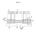
- FIG. 4 shows a magnified top plan view of a side portion (A) in a periphery of FIG. 1
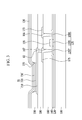
- FIG. 5 shows a cross-sectional view with respect to a line V-V of FIG. 4
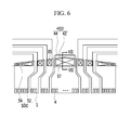
- FIG. 6 shows a magnified top plan view of a side portion (B) in a periphery of FIG. 1
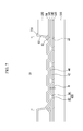
- FIG. 7 shows cross-sectional view with respect to a line VII-VII of FIG. 6 .
- a buffer layer 120 is formed on the substrate 100 of the organic light emitting diode (OLED) display.
- a portion in which a contact hole for transmitting a common voltage to a second electrode of a pixel from the outside (or an external circuit) will be called a contact area (LA).
- the contact area (LA) is provided on a side portion A and a side portion B of the periphery (PB), shown in FIG. 1 .
- Each contact area (LA) is provided on the side portion A and the side portion B in FIG. 4 , and a plurality of contact areas (LA) can be formed thereon.
- the buffer layer 120 includes an opening 22 from which a portion of the buffer layer 120 that corresponds to the contact area (LA) is removed, and a plurality of protrusions 600 are formed in the opening 22.
- each protrusion 600 includes a first protrusion 62 made of the same material as the buffer layer 120, and a second protrusion 64 provided on the first protrusion and made of the same material as the semiconductor.
- the first protrusion 62 can be considered to be a first portion of each protrusion 600
- the second protrusion 62 can be considered to be a second portion 64 of each protrusion 600.
- the protrusion 600 may extend in a direction (e.g., a direction perpendicular to a cutting plane) to form a rib, or may be shaped as an island type protrusion.
- a plurality of buffer layers 120 can be formed, for example increasing the height of the portion of the protrusion 600 made of the same material as the buffer layers 120.
- the height (H) of the protrusion 600 can be 300 nm (3000 ⁇ ) to 500 nm (5000 ⁇ ) in consideration of step coverage of the upper layer.
- the first protrusion 62 is formed to be 300 nm (3000 ⁇ ) to 450 nm (4500 ⁇ ) thick
- the second protrusion 64 is formed to be 50 nm (500 ⁇ ) thick.
- a gate insulating layer 140 is formed on the buffer layer 120 and the protrusions 600.
- the gate insulating layer 140 is formed along the protrusions 600 to form protrusions and depressions.
- the protrusions and depressions in the gate insulating layer 140 correspond to the shape of the protrusions 600.
- a gate common voltage line 42 and a gate driving voltage line 52 are formed on the gate insulating layer 140.
- the gate common voltage line 42 is formed along the protrusions and depressions formed by the protrusions 600 to thus form protrusions and depressions.
- the protrusions and depressions in the gate common voltage line 42 correspond to the shape of the protrusions 600.
- the gate common voltage line 42 and the gate driving voltage line 52 are formed on the same layer as the gate line, and they can be made of the same material as the gate line.
- the gate common voltage line 42 and the gate driving voltage line 52 respectively receive a common voltage and a driving voltage from a flexible printed circuit (FPC) through pads 4 and 5.
- FPC flexible printed circuit
- a first interlayer insulating layer 160 is formed on the gate common voltage line 42 and the gate driving voltage line 52.
- the first interlayer insulating layer 160 includes common voltage contact holes 83 for exposing the gate common voltage line 42 and driving voltage contact holes 85 for exposing the gate driving voltage line 52.
- a data common voltage line 44 connected to the gate common voltage line 42 in the region of the common voltage contact hole 83 and a data driving voltage line 54 connected to the gate driving voltage line 52 through the driving voltage contact hole 85 are formed on the first interlayer insulating layer 160.
- the data common voltage line 44 is formed along the protrusions and depressions of the gate common voltage line 42 to thus form protrusions and depressions.
- the protrusions and depressions in the data common voltage line 44 correspond to the protrusions and depressions of the gate common voltage line 42.
- An area that contacts the gate common voltage line 42 is increased by the protrusions and depressions, thereby reducing contact resistance.
- a barrier rib 190 is formed on the data common voltage line 44 and the data driving voltage line 54
- the barrier rib 190 has a common voltage opening 97 for exposing the data common voltage line 44.
- the common voltage opening 97 is provided in the contact area (LA).
- a second electrode 730 is formed on the barrier rib 190.
- the second electrode 730 is connected to the data common voltage line 44 in the region of the common voltage opening 97.
- the common voltage applied through the pad 4 is transmitted to the second electrode 730 through a common voltage line 400 configured by the gate common voltage line 42 and the data common voltage line 44.
- a contact area of the second electrode 730 with the data common voltage line 44 is increased by the protrusions and depressions of the contact area (LA) formed by the protrusions 600, so the second electrode 730 and the data common voltage line 44 are strongly combined and contact resistance is reduced. Therefore, heat is not generated when an incised portion of the barrier rib 190 configuring the common voltage opening 97 is lifted.
- the constant voltage applied through the pad 5 is transmitted to the driving voltage line through a driving voltage line 500 configured by the gate driving voltage line 52 and the data driving voltage line 54.
- FIG. 8 shows a cross-sectional view of a side portion (B), shown in FIG. 1 , in a periphery according to another exemplary embodiment.
- An interlayer configuration is generally equivalent to that of FIG. 3 to FIG. 7 so different parts will be described in detail.
- the substrate 100 in the contact area (LA) has a plurality of recess portions (U).
- the recess portions (U) are provided between the protrusions 600, and the recess portions (U) increase the step height of the protrusions (600).
- the recess portion (U) may not be formed in the substrate 100.
- an organic light emitting diode display comprising: a pixel unit formed on a substrate and including an organic light emitting diode for displaying an image; and a periphery region surrounding the pixel unit, the periphery region comprising: a gate common voltage line formed on the substrate, the gate common voltage line arranged to receive a common voltage from an external circuit, an interlayer insulating layer arranged to cover part of the gate common voltage line and including a common voltage contact hole for exposing a part of the gate common voltage line, a data common voltage line formed on the interlayer insulating layer and contacting the gate common voltage line in the region of the common voltage contact hole, a barrier rib arranged to cover part of the data common voltage line and including a common voltage opening for exposing a part of the data common voltage line, a common electrode formed on the barrier rib and contacting the data common voltage line in the region of the common voltage opening, and a plurality of protrusions provided in the region of the common voltage
- the gate common voltage line and the data common voltage line contact each other. Furthermore, in the region of the common voltage contact hole, the gate common voltage line and the data common voltage line are both formed over the plurality of protrusions. Thus, the common voltage line and the data common voltage line are formed with a series of protrusions and depressions corresponding to the shape of the plurality of protrusions.
- the substrate includes a plurality of recess portions respectively provided between neighboring protrusions in the region of the common voltage contact hole.
- the plurality of recess portions can increase the effective height of the protrusions.
- the pixel unit includes a thin film transistor for connecting the second electrode to a drain electrode.
- each protrusion comprises a material that includes a material of a semiconductor of the thin film transistor.
- the each protrusion can be made out of the semiconductor material used in the thin film transistor. In such arrangements, each protrusion can be deposited at the same time as the semiconductor material.
- the organic light emitting diode display can comprise a buffer layer formed on the substrate.
- each protrusion can be made of the same material as the buffer layer.
- each protrusion can include a first portion made of the same material as the buffer layer, and a second portion provided on the first portion and made of the same material as the semiconductor.
- each protrusion is provided in the form of a rib on the substrate. In other embodiments, the protrusions can take different forms.
Landscapes
- Engineering & Computer Science (AREA)
- Microelectronics & Electronic Packaging (AREA)
- Electroluminescent Light Sources (AREA)
- Devices For Indicating Variable Information By Combining Individual Elements (AREA)
Applications Claiming Priority (1)
| Application Number | Priority Date | Filing Date | Title |
|---|---|---|---|
| KR1020120137356A KR101398448B1 (ko) | 2012-11-29 | 2012-11-29 | 유기 발광 표시 장치 |
Publications (2)
| Publication Number | Publication Date |
|---|---|
| EP2747062A2 true EP2747062A2 (de) | 2014-06-25 |
| EP2747062A3 EP2747062A3 (de) | 2017-03-22 |
Family
ID=49667070
Family Applications (1)
| Application Number | Title | Priority Date | Filing Date |
|---|---|---|---|
| EP13194955.4A Withdrawn EP2747062A3 (de) | 2012-11-29 | 2013-11-28 | Organische lichtemittierende Diodenanzeige |
Country Status (5)
| Country | Link |
|---|---|
| US (1) | US9064833B2 (de) |
| EP (1) | EP2747062A3 (de) |
| KR (1) | KR101398448B1 (de) |
| CN (1) | CN103855190B (de) |
| TW (1) | TWI604597B (de) |
Cited By (1)
| Publication number | Priority date | Publication date | Assignee | Title |
|---|---|---|---|---|
| EP4221485A1 (de) * | 2014-07-08 | 2023-08-02 | LG Display Co., Ltd. | Organische lichtemittierende anzeigevorrichtung und herstellungsverfahren dafür |
Families Citing this family (25)
| Publication number | Priority date | Publication date | Assignee | Title |
|---|---|---|---|---|
| JP2016004910A (ja) * | 2014-06-17 | 2016-01-12 | キヤノン株式会社 | 有機発光装置 |
| CN105336869A (zh) * | 2014-07-22 | 2016-02-17 | 上海和辉光电有限公司 | 电极结构及oled显示器 |
| KR102300404B1 (ko) | 2015-01-14 | 2021-09-09 | 삼성디스플레이 주식회사 | 유기 발광 표시 장치 |
| KR102315889B1 (ko) * | 2015-04-14 | 2021-10-21 | 삼성디스플레이 주식회사 | 표시 패널 |
| KR102393931B1 (ko) * | 2015-05-01 | 2022-05-04 | 삼성디스플레이 주식회사 | 유기 발광 표시 장치 |
| CN104882467B (zh) * | 2015-06-04 | 2017-12-15 | 京东方科技集团股份有限公司 | 基板及其制造方法、显示装置 |
| KR102477299B1 (ko) | 2015-06-12 | 2022-12-14 | 삼성디스플레이 주식회사 | 디스플레이 장치 |
| KR102526110B1 (ko) | 2016-04-12 | 2023-04-27 | 삼성디스플레이 주식회사 | 표시 장치 및 표시 장치의 제조 방법 |
| KR102572341B1 (ko) * | 2016-07-29 | 2023-08-30 | 엘지디스플레이 주식회사 | 표시장치 |
| US10270055B2 (en) | 2017-03-16 | 2019-04-23 | Wuhan China Star Optoelectronics Technology Co., Ltd. | Flexible display device and method of manufacturing the same |
| CN106848102A (zh) * | 2017-03-16 | 2017-06-13 | 武汉华星光电技术有限公司 | 一种柔性显示器件及其制备方法 |
| CN107068727A (zh) * | 2017-05-05 | 2017-08-18 | 京东方科技集团股份有限公司 | 显示基板和显示装置 |
| CN107180837A (zh) * | 2017-05-17 | 2017-09-19 | 京东方科技集团股份有限公司 | 一种阵列基板及其制作方法、显示装置 |
| KR102492735B1 (ko) | 2017-09-12 | 2023-01-27 | 삼성디스플레이 주식회사 | 표시 장치 |
| KR102441783B1 (ko) | 2017-12-05 | 2022-09-08 | 삼성디스플레이 주식회사 | 표시 장치 및 그 제조 방법 |
| CN108493200A (zh) * | 2018-05-28 | 2018-09-04 | 武汉华星光电半导体显示技术有限公司 | 一种阵列基板的制作方法、阵列基板及显示装置 |
| TWI662341B (zh) * | 2018-05-31 | 2019-06-11 | 友達光電股份有限公司 | 顯示裝置 |
| CN109037279B (zh) * | 2018-07-23 | 2020-10-16 | 武汉华星光电半导体显示技术有限公司 | 一种显示面板 |
| US11069668B2 (en) * | 2018-09-09 | 2021-07-20 | Innolux Corporation | Electronic device for reducing a border edge of the non-display areas |
| KR102075741B1 (ko) * | 2018-12-17 | 2020-02-10 | 엘지디스플레이 주식회사 | 표시패널 |
| CN110323196B (zh) * | 2019-05-09 | 2021-11-16 | 京东方科技集团股份有限公司 | 一种显示基板及其制备方法、显示装置 |
| CN110265467A (zh) | 2019-06-28 | 2019-09-20 | 京东方科技集团股份有限公司 | 阵列基板及其制造方法、显示面板和显示装置 |
| TWI709126B (zh) * | 2019-11-15 | 2020-11-01 | 友達光電股份有限公司 | 顯示裝置 |
| KR20220067649A (ko) | 2020-11-17 | 2022-05-25 | 삼성디스플레이 주식회사 | 표시 장치 |
| JP2023106165A (ja) * | 2022-01-20 | 2023-08-01 | 株式会社ジャパンディスプレイ | 表示装置 |
Family Cites Families (15)
| Publication number | Priority date | Publication date | Assignee | Title |
|---|---|---|---|---|
| KR100637147B1 (ko) * | 2004-02-17 | 2006-10-23 | 삼성에스디아이 주식회사 | 박막의 밀봉부를 갖는 유기 전계 발광 표시장치, 그제조방법 및 막 형성장치 |
| KR100671638B1 (ko) | 2006-01-26 | 2007-01-19 | 삼성에스디아이 주식회사 | 유기 전계 발광 표시장치 |
| KR100897157B1 (ko) | 2008-02-28 | 2009-05-14 | 삼성모바일디스플레이주식회사 | 유기전계발광 표시장치 |
| KR101493086B1 (ko) * | 2008-05-16 | 2015-02-13 | 엘지디스플레이 주식회사 | 유기발광 표시장치 및 그 제조 방법 |
| JP2010117549A (ja) | 2008-11-13 | 2010-05-27 | Seiko Epson Corp | 表示装置の製造方法 |
| KR101677266B1 (ko) * | 2010-02-12 | 2016-11-18 | 삼성디스플레이 주식회사 | 유기 발광 표시 장치 및 이의 제조 방법 |
| KR101275792B1 (ko) * | 2010-07-28 | 2013-06-18 | 삼성디스플레이 주식회사 | 표시 장치 및 유기 발광 표시 장치 |
| KR101769586B1 (ko) * | 2010-09-24 | 2017-08-21 | 삼성디스플레이 주식회사 | 유기 발광 디스플레이 장치 |
| KR101764272B1 (ko) * | 2010-12-02 | 2017-08-16 | 삼성디스플레이 주식회사 | 유기 발광 표시 장치 및 그 제조방법 |
| KR101822012B1 (ko) * | 2010-12-07 | 2018-01-26 | 삼성디스플레이 주식회사 | 유기전계발광 표시 장치 및 그 제조 방법 |
| JP5639514B2 (ja) * | 2011-03-24 | 2014-12-10 | 株式会社東芝 | 表示装置 |
| KR101877451B1 (ko) | 2011-10-17 | 2018-07-12 | 삼성디스플레이 주식회사 | 유기 발광 표시 장치 |
| KR101924996B1 (ko) * | 2012-03-29 | 2018-12-05 | 삼성디스플레이 주식회사 | 유기 발광 표시 장치 |
| KR101930847B1 (ko) | 2012-05-16 | 2018-12-20 | 삼성디스플레이 주식회사 | 유기 발광 표시 장치 및 그 제조방법 |
| KR101967407B1 (ko) * | 2012-10-08 | 2019-04-10 | 삼성디스플레이 주식회사 | 유기 발광 표시 장치 |
-
2012
- 2012-11-29 KR KR1020120137356A patent/KR101398448B1/ko active Active
-
2013
- 2013-11-26 TW TW102143120A patent/TWI604597B/zh active
- 2013-11-28 EP EP13194955.4A patent/EP2747062A3/de not_active Withdrawn
- 2013-11-29 US US14/093,270 patent/US9064833B2/en active Active
- 2013-11-29 CN CN201310629805.8A patent/CN103855190B/zh active Active
Non-Patent Citations (1)
| Title |
|---|
| None |
Cited By (1)
| Publication number | Priority date | Publication date | Assignee | Title |
|---|---|---|---|---|
| EP4221485A1 (de) * | 2014-07-08 | 2023-08-02 | LG Display Co., Ltd. | Organische lichtemittierende anzeigevorrichtung und herstellungsverfahren dafür |
Also Published As
| Publication number | Publication date |
|---|---|
| US9064833B2 (en) | 2015-06-23 |
| US20140145171A1 (en) | 2014-05-29 |
| EP2747062A3 (de) | 2017-03-22 |
| TWI604597B (zh) | 2017-11-01 |
| TW201423961A (zh) | 2014-06-16 |
| KR101398448B1 (ko) | 2014-05-30 |
| CN103855190A (zh) | 2014-06-11 |
| CN103855190B (zh) | 2018-05-01 |
Similar Documents
| Publication | Publication Date | Title |
|---|---|---|
| US9064833B2 (en) | Organic light emitting diode display | |
| EP2835831B1 (de) | Organische lichtemittierende Diodenanzeige | |
| US10971574B2 (en) | Display device | |
| US9070896B2 (en) | Organic light emitting diode display | |
| CN103811675B (zh) | 柔性有机电致发光装置及其制造方法 | |
| KR102280959B1 (ko) | 표시장치 및 그 제조 방법 | |
| US8040051B2 (en) | Organic light emitting display and method of manufacturing the same | |
| JP6756560B2 (ja) | 表示装置 | |
| JP2018097361A (ja) | 有機発光表示装置およびその製造方法 | |
| CN102456846B (zh) | 有机发光显示装置 | |
| US11653547B2 (en) | Display device | |
| JP4832781B2 (ja) | 有機エレクトロルミネッセンス表示装置 | |
| US8841832B2 (en) | Organic light emitting diode display having improved strength by preventing the exfoliation of a sealant | |
| KR20120063219A (ko) | 반사 전극을 구비한 유기전계발광 표시장치 제조 방법 | |
| KR101796934B1 (ko) | 반사 전극을 구비한 유기전계발광 표시장치 및 그 제조 방법 | |
| US8610123B2 (en) | Organic light emitting diode display and manufacturing method thereof | |
| KR102515631B1 (ko) | 유기 발광 표시 장치 | |
| US10573205B2 (en) | Flexible display device and method for manufacturing flexible display device | |
| KR101587822B1 (ko) | 유기전계발광 표시장치 및 그 제조 방법 | |
| US12207503B2 (en) | Display device | |
| US20250268067A1 (en) | Display Device | |
| KR20130011707A (ko) | 표시장치 및 그 제조방법 | |
| KR20160083641A (ko) | 유기전계 발광소자 |
Legal Events
| Date | Code | Title | Description |
|---|---|---|---|
| PUAI | Public reference made under article 153(3) epc to a published international application that has entered the european phase |
Free format text: ORIGINAL CODE: 0009012 |
|
| 17P | Request for examination filed |
Effective date: 20131128 |
|
| AK | Designated contracting states |
Kind code of ref document: A2 Designated state(s): AL AT BE BG CH CY CZ DE DK EE ES FI FR GB GR HR HU IE IS IT LI LT LU LV MC MK MT NL NO PL PT RO RS SE SI SK SM TR |
|
| AX | Request for extension of the european patent |
Extension state: BA ME |
|
| RAP1 | Party data changed (applicant data changed or rights of an application transferred) |
Owner name: SAMSUNG DISPLAY CO., LTD. |
|
| PUAL | Search report despatched |
Free format text: ORIGINAL CODE: 0009013 |
|
| AK | Designated contracting states |
Kind code of ref document: A3 Designated state(s): AL AT BE BG CH CY CZ DE DK EE ES FI FR GB GR HR HU IE IS IT LI LT LU LV MC MK MT NL NO PL PT RO RS SE SI SK SM TR |
|
| AX | Request for extension of the european patent |
Extension state: BA ME |
|
| RIC1 | Information provided on ipc code assigned before grant |
Ipc: H01L 27/00 20060101AFI20170213BHEP |
|
| STAA | Information on the status of an ep patent application or granted ep patent |
Free format text: STATUS: REQUEST FOR EXAMINATION WAS MADE |
|
| R17P | Request for examination filed (corrected) |
Effective date: 20170922 |
|
| RBV | Designated contracting states (corrected) |
Designated state(s): AL AT BE BG CH CY CZ DE DK EE ES FI FR GB GR HR HU IE IS IT LI LT LU LV MC MK MT NL NO PL PT RO RS SE SI SK SM TR |
|
| STAA | Information on the status of an ep patent application or granted ep patent |
Free format text: STATUS: EXAMINATION IS IN PROGRESS |
|
| 17Q | First examination report despatched |
Effective date: 20180528 |
|
| STAA | Information on the status of an ep patent application or granted ep patent |
Free format text: STATUS: THE APPLICATION IS DEEMED TO BE WITHDRAWN |
|
| 18D | Application deemed to be withdrawn |
Effective date: 20200310 |