EP2747121A1 - Sekundärelektronenoptik und -detektionsvorrichtung - Google Patents
Sekundärelektronenoptik und -detektionsvorrichtung Download PDFInfo
- Publication number
- EP2747121A1 EP2747121A1 EP12198963.6A EP12198963A EP2747121A1 EP 2747121 A1 EP2747121 A1 EP 2747121A1 EP 12198963 A EP12198963 A EP 12198963A EP 2747121 A1 EP2747121 A1 EP 2747121A1
- Authority
- EP
- European Patent Office
- Prior art keywords
- deflector
- charged particle
- focusing lens
- bender
- detection element
- Prior art date
- Legal status (The legal status is an assumption and is not a legal conclusion. Google has not performed a legal analysis and makes no representation as to the accuracy of the status listed.)
- Withdrawn
Links
Images




Classifications
-
- H—ELECTRICITY
- H01—ELECTRIC ELEMENTS
- H01J—ELECTRIC DISCHARGE TUBES OR DISCHARGE LAMPS
- H01J37/00—Discharge tubes with provision for introducing objects or material to be exposed to the discharge, e.g. for the purpose of examination or processing thereof
- H01J37/26—Electron or ion microscopes; Electron or ion diffraction tubes
-
- H—ELECTRICITY
- H01—ELECTRIC ELEMENTS
- H01J—ELECTRIC DISCHARGE TUBES OR DISCHARGE LAMPS
- H01J37/00—Discharge tubes with provision for introducing objects or material to be exposed to the discharge, e.g. for the purpose of examination or processing thereof
- H01J37/02—Details
- H01J37/244—Detectors; Associated components or circuits therefor
-
- G—PHYSICS
- G01—MEASURING; TESTING
- G01N—INVESTIGATING OR ANALYSING MATERIALS BY DETERMINING THEIR CHEMICAL OR PHYSICAL PROPERTIES
- G01N23/00—Investigating or analysing materials by the use of wave or particle radiation, e.g. X-rays or neutrons, not covered by groups G01N3/00 – G01N17/00, G01N21/00 or G01N22/00
- G01N23/22—Investigating or analysing materials by the use of wave or particle radiation, e.g. X-rays or neutrons, not covered by groups G01N3/00 – G01N17/00, G01N21/00 or G01N22/00 by measuring secondary emission from the material
- G01N23/225—Investigating or analysing materials by the use of wave or particle radiation, e.g. X-rays or neutrons, not covered by groups G01N3/00 – G01N17/00, G01N21/00 or G01N22/00 by measuring secondary emission from the material using electron or ion
-
- H—ELECTRICITY
- H01—ELECTRIC ELEMENTS
- H01J—ELECTRIC DISCHARGE TUBES OR DISCHARGE LAMPS
- H01J37/00—Discharge tubes with provision for introducing objects or material to be exposed to the discharge, e.g. for the purpose of examination or processing thereof
- H01J37/02—Details
- H01J37/04—Arrangements of electrodes and associated parts for generating or controlling the discharge, e.g. electron-optical arrangement or ion-optical arrangement
- H01J37/147—Arrangements for directing or deflecting the discharge along a desired path
-
- H—ELECTRICITY
- H01—ELECTRIC ELEMENTS
- H01J—ELECTRIC DISCHARGE TUBES OR DISCHARGE LAMPS
- H01J37/00—Discharge tubes with provision for introducing objects or material to be exposed to the discharge, e.g. for the purpose of examination or processing thereof
- H01J37/26—Electron or ion microscopes; Electron or ion diffraction tubes
- H01J37/261—Details
-
- H—ELECTRICITY
- H01—ELECTRIC ELEMENTS
- H01J—ELECTRIC DISCHARGE TUBES OR DISCHARGE LAMPS
- H01J37/00—Discharge tubes with provision for introducing objects or material to be exposed to the discharge, e.g. for the purpose of examination or processing thereof
- H01J37/26—Electron or ion microscopes; Electron or ion diffraction tubes
- H01J37/28—Electron or ion microscopes; Electron or ion diffraction tubes with scanning beams
-
- H—ELECTRICITY
- H01—ELECTRIC ELEMENTS
- H01J—ELECTRIC DISCHARGE TUBES OR DISCHARGE LAMPS
- H01J2237/00—Discharge tubes exposing object to beam, e.g. for analysis treatment, etching, imaging
- H01J2237/05—Arrangements for energy or mass analysis
- H01J2237/057—Energy or mass filtering
-
- H—ELECTRICITY
- H01—ELECTRIC ELEMENTS
- H01J—ELECTRIC DISCHARGE TUBES OR DISCHARGE LAMPS
- H01J2237/00—Discharge tubes exposing object to beam, e.g. for analysis treatment, etching, imaging
- H01J2237/15—Means for deflecting or directing discharge
- H01J2237/151—Electrostatic means
- H01J2237/1516—Multipoles
-
- H—ELECTRICITY
- H01—ELECTRIC ELEMENTS
- H01J—ELECTRIC DISCHARGE TUBES OR DISCHARGE LAMPS
- H01J2237/00—Discharge tubes exposing object to beam, e.g. for analysis treatment, etching, imaging
- H01J2237/244—Detection characterized by the detecting means
- H01J2237/2446—Position sensitive detectors
- H01J2237/24465—Sectored detectors, e.g. quadrants
-
- H—ELECTRICITY
- H01—ELECTRIC ELEMENTS
- H01J—ELECTRIC DISCHARGE TUBES OR DISCHARGE LAMPS
- H01J2237/00—Discharge tubes exposing object to beam, e.g. for analysis treatment, etching, imaging
- H01J2237/244—Detection characterized by the detecting means
- H01J2237/2449—Detector devices with moving charges in electric or magnetic fields
-
- H—ELECTRICITY
- H01—ELECTRIC ELEMENTS
- H01J—ELECTRIC DISCHARGE TUBES OR DISCHARGE LAMPS
- H01J2237/00—Discharge tubes exposing object to beam, e.g. for analysis treatment, etching, imaging
- H01J2237/245—Detection characterised by the variable being measured
- H01J2237/24592—Inspection and quality control of devices
-
- H—ELECTRICITY
- H01—ELECTRIC ELEMENTS
- H01J—ELECTRIC DISCHARGE TUBES OR DISCHARGE LAMPS
- H01J2237/00—Discharge tubes exposing object to beam, e.g. for analysis treatment, etching, imaging
- H01J2237/26—Electron or ion microscopes
- H01J2237/28—Scanning microscopes
- H01J2237/2803—Scanning microscopes characterised by the imaging method
- H01J2237/2806—Secondary charged particle
-
- H—ELECTRICITY
- H01—ELECTRIC ELEMENTS
- H01J—ELECTRIC DISCHARGE TUBES OR DISCHARGE LAMPS
- H01J2237/00—Discharge tubes exposing object to beam, e.g. for analysis treatment, etching, imaging
- H01J2237/26—Electron or ion microscopes
- H01J2237/28—Scanning microscopes
- H01J2237/2812—Emission microscopes
-
- H—ELECTRICITY
- H01—ELECTRIC ELEMENTS
- H01J—ELECTRIC DISCHARGE TUBES OR DISCHARGE LAMPS
- H01J2237/00—Discharge tubes exposing object to beam, e.g. for analysis treatment, etching, imaging
- H01J2237/26—Electron or ion microscopes
- H01J2237/28—Scanning microscopes
- H01J2237/2813—Scanning microscopes characterised by the application
- H01J2237/2814—Measurement of surface topography
Definitions
- Embodiments of the present invention relate to charged particle beam devices, for example, for inspection system applications, testing system applications, lithography system applications, defect review or critical dimensioning applications or the like.
- they relate to secondary beam optics and a detection device.
- embodiments relate to a secondary charged particle detection system for a charged particle beam device and a method of detection of secondary charged particles in a charged particle beam device.
- Particle detectors e.g. electron detectors
- charged particle beam systems e.g. electron microscopes for Electron Beam Inspection (EBI), Defect Review or Critical Dimension measurement, Focused Ion Beam systems etc.
- Charged particle beam apparatuses have many functions in a plurality of industrial fields, including, but not limited to, inspection of semiconductor devices during manufacturing, exposure systems for lithography, detecting devices and testing systems. Thus, there is a high demand for structuring and inspecting specimens within the micrometer and nanometer scale.
- Micrometer and nanometer scale process control, inspection or structuring is often done with charged particle beams, e.g. electron beams, which are generated and focused in charged particle beam devices, such as scanning electron microscopes or electron beam pattern generators.
- charged particle beams offer superior spatial resolution compared to, e.g. photon beams, due to their short wavelengths. Also other types of charged particles, e.g. positive ions, could be detected by the device in a variety of different instruments.
- secondary electrons Upon irradiation of a sample by a primary beam of electrons, secondary electrons (SE) are created which carry information about the topography of the sample, its chemical constituents, its electrostatic potential and other information.
- SE secondary electrons
- all of the SE are collected and lead to a sensor, usually a scintillator, a pin diode or the like.
- An image is created where the gray level is proportional to the number of electrons collected.
- BF detector In EBI this kind of Bright Field (BF) detector is also used. However, an increase in sensitivity to changes in topography or surface potential (voltage contrast - VC) is desired.
- VC can be enhanced by energy filtering the SE signal, while topography information resulting from physical defects can be enhanced by using multiple sensors that collect only SE within certain ranges of take-off angles at the sample.
- this can be done by an optical system consisting of a beam splitter 15 that separates the primary beam 130 and the SE bundle 140, a beam bender 440 that deflects the SE bundle to a large angle (typically 90° for horizontal exit), SE focus lens 301 and an alignment deflector 902 for focusing and aligning the beam to the sensor.
- the imaging information is increased while high-speed detection is provided.
- SE secondary electrons
- High speed detection provided with topography information and/or information on the energy of the secondary particles is a challenging task, for which continuous improvement is desired. Accordingly, improvements of the detection in the SEM-based tools, particularly in high throughput defect inspection or review tools, are desired. Thereby, enhanced imaging contrast is an important aspect for high throughput metrology and inspection.
- the object of the present invention is therefore to provide a SE optics and a detection device with improved features while keeping the number of optical elements and the related power supplies as low as possible.
- a secondary charged particle detection system for a charged particle beam device according to claim 1 a charged particle beam device, including a secondary charged particle detection system according to claim 9 and a method of detection of secondary charged particles in a charged particle beam device according to claim 10 are provided.
- a secondary charged particle detection system for a charged particle beam device.
- the detection system includes a beam splitter for separating a primary beam and a secondary beam formed upon impact on a specimen; a beam bender for deflecting the secondary beam; a focusing lens for focusing the secondary beam; a detection element for detecting the secondary beam particles, and three deflection elements, wherein at least a first deflector is provided between the beam bender and the focusing lens, at least a second deflector is provided between the focusing lens and the detection element, at least a third deflector is provided between the beam splitter and the detection element.
- a method of detection of secondary charged particles in a charged particle beam device includes separating a secondary beam from a primary beam by means of a beam separator; deflecting the separated secondary beam by means of a main deflector; and focusing the secondary beam on a detection element by means of a focusing lens; wherein the secondary beam is deflected by at least a first deflector provided between the beam bender and the focusing lens, at least a second deflector provided between the focusing lens and the detection element, and at least a third deflector provided between the beam splitter and the detection element.
- Embodiments are also directed to apparatuses for carrying out the disclosed methods and including apparatus parts for performing each described method step. These method steps may be performed by way of hardware components, a computer programmed by appropriate software, by any combination of the two or in any other manner. Furthermore, embodiments are also directed to methods by which the described apparatus operates. It includes method steps for carrying out every function of the apparatus or manufacturing every part of the apparatus.
- the charged particle beam device or components thereof will exemplarily be referred to as a charged particle beam device including the detection of secondary electrons or backscattered electrons.
- SE secondary electrons
- SE secondary electrons
- a "specimen” as referred to herein includes, but is not limited to, semiconductor wafers, semiconductor workpieces, and other workpieces such as memory disks and the like. Embodiments of the invention may be applied to any workpiece on which material is deposited or which are structured.
- a specimen includes a surface to be structured or on which layers are deposited, an edge, and typically a bevel.
- a secondary charged particle detection system for a charged particle beam device.
- the detection system includes a beam splitter for separating a primary beam and a secondary beam formed upon impact on a specimen; a beam bender for deflecting the secondary beam; a focusing lens for focusing the secondary beam; a detection element for detecting the secondary beam particles, and three deflection elements, wherein at least a first deflector is provided between the beam bender and the focusing lens, at least a second deflector is provided between the focusing lens and the detection element, at least a third deflector is provided between the beam splitter and the detection element.
- an improved secondary electron optics is provided.
- contrast is one of the key factors for faster inspection, i.e. higher throughput during inspection of wafers, specimen or the like.
- this is important, because, for example on a 300 mm wafer defects having a size of 40 nm need to be detected, which, thus, have only 5.6*10 -16 times the size of the entire area to be scanned.
- the secondary electron optics shown in figure 1 does not provide for energy filtering and detectors, wherein filtering depending upon the starting angle of the secondary electrons can be conducted.
- the hemispherical beam bender can provide stigmatic focusing for a specific set of operation conditions. Thus, no independent stigmation control can be provided.
- the specific set of operation conditions also limits the flexibility to align the secondary beam, which exits the beam bender, with respect to the secondary electron focusing lens. The scanning of the primary electron beam on the specimen, for example with large field a view, results in movement of the secondary electron beam bundle.
- FIG. 2 shows a charged particle beam device 200, which includes a secondary electron optics according to embodiments described herein.
- the device includes a charged particle source 105 producing a primary beam 130 which is directed towards a specimen 13 through an objective lens 10. Particles released from or backscattered from the specimen form a secondary beam 140 carrying information about the specimen.
- Fig. 2 shows a secondary charged particle detection system for a charged particle beam device according to an embodiment.
- the secondary beam 140 is separated from the primary beam 130 by means of a beam separator 15 and enters a beam bender 440.
- the beam separator can, for example, include at least one magnetic deflector, a Wien filter, or any other means, wherein the electrons are directed away from the primary beam, e.g. due to the velocity depending Lorenz force.
- the beam bender 440 deflects the secondary beam 140 towards a focusing lens 301.
- the focusing lens 301 focuses secondary beam 140 on a detection element or sensor 222 (scintillator, pin diode etc.) of a detector assembly 220.
- the detection system according to embodiments illustrated, for example with respect to FIG. 2 , allows to focus the secondary particle bundle on a detector for Bright Field (BF) imaging, to adapt the size of the secondary particle bundle, or to adapt the size of the secondary particle bundle to a segmented detector in order to achieve angular resolution as described in more detail below.
- BF Bright Field
- three deflectors 903, 901, and 903 are provided along the path of the secondary beam.
- a secondary charged particle detection system for a charged particle beam device.
- the detection system includes a beam splitter for separating a primary beam and a secondary beam formed upon impact on a specimen; a beam bender for deflecting the secondary beam; a focusing lens for focusing the secondary beam; a detection element for detecting the secondary beam particles, and three deflection elements, wherein at least a first deflector is provided between the beam bender and the focusing lens, at least a second deflector is provided between the focusing lens and the detection element, at least a third deflector is provided between the beam splitter and the beam bender.
- a first deflector 901 is arranged between the beam bender 440 and the focusing lens 301, a second deflector 902 is provided between the focusing lens 301 and the detection element 222, and a third deflector 903 is provided between the beam splitter 15 and the beam bender 440.
- the third deflector is the first one of the three deflectors through which the SE pass the embodiments described with respect to Fig. 2 .
- This arrangement of the deflectors has the advantage that the deflector, for which the electrons pass first, i.e. the third deflector 903, is provided as soon as possible after separation of the primary beam and the secondary beam.
- the SE bundle When scanning a large Field of View (FOV) with the primary beam, the SE bundle starts moving accordingly and , in general, the SE bundle is scanning across the sensor. For small sensors this may lead to signal loss towards the edges of the FOV. In angular filtering mode it may result in sensitivity variations across the FOV. In energy filtering mode it may change the filtering threshold across the FOV. To avoid these effects, a de-scanning (anti scan, counter scan) signal needs to be applied to the SE bundle by the SE optics according to embodiments described herein, where three deflectors are provided for improved SE signal capturing.
- FOV Field of View
- the counter scan is provided before the SE bundle enters the SE focus lens and/or a potentially existing filtering device.
- two deflectors are provided before the lens in order to allow for alignment onto the axis and along the axis of the SE optics before entering the focus lens 301.
- focusing and angular / energy resolution will depend on the PE beam position in the FOV.
- the focusing lens is an einzel-lens. According to an embodiment the focusing lens is in a deceleration mode, to keep a necessary focusing voltage low. According to yet further embodiments, which can be combined with other embodiments, described herein the focus lens 301 is closer to the sensor as compared to known SE optics, thus acting as a transfer lens of magnification ⁇ 1. This avoids introducing additional magnification and unnecessary amplification of the unwanted movement of the SE bundle during scan can be reduced. Further, shifting the focus lens closer to the sensor will also reduce the necessary focus voltage.
- the beam bender 440 is a hemispherical beam bender.
- the beam bender includes two approximately spherical and approximately concentric electrodes creating a large angle deflection field with approximately stigmatic focusing, if properly excited by two voltages (Vbend pos and Vbend neg).
- Vbend pos and Vbend neg The deviation from the spherical shape and the relative position of the electrodes can be designed such that no hexapole component is created.
- the beam bender voltages are set such that the required total deflection angle, e.g. 90°, is reached and the focusing is approximately stigmatic.
- the hemispherical beam bender typically focuses the first SE crossover above the objective lens stigmatically into a second crossover in front of the SE focus lens. This is a rough alignment onto the optical axis of the SE focus lens after the secondary beam exits the beam bender.
- the third deflector 903 which is the first deflector through which the SEs pass, this can only be provided for a specific choice of the bending voltages Vbend pos and Vbend neg, which might conflict with other requirements, e.g. stigmation.
- the hemispherical sector generally does not have an independent stigmation control, unless provided with the SE optics according to any of the embodiments described herein.
- the same reasoning applies for the following consideration, wherein the hemispherical beam bender should typically be provided to align the optical axis of the SE bundle to the optical axis of the SE optics for any arbitrary choice of landing energy Epe of the primary electron beam.
- the deflectors can provide at least dipole deflection fields in two directions, e.g. one in the paper plane of the figures and one orthogonal to the paper plane in the figures. Accordingly, according to the embodiments described herein, the deflectors provide at least two-dimensional deflection.
- the optical axis will generally be off-center in 1 direction and tilted in both directions. As a consequence, optical quality of the imaging will be not as good as possible. Accordingly, a common SE optics does not provide independent alignment to the SE focus lens in two orthogonal directions unless provided with the SE optics according to any of the embodiments described herein
- the third deflector 903 is adapted to generate orthogonal deflection fields with the ability to add a counter scan signal.
- the first deflector 901 is adapted to generate orthogonal dipole deflection fields.
- the generation of higher order multipoles in this element might not be highly effective, since a SE-crossover is formed near the element. However, it could also have a larger number of poles, e.g. 8, because a potential correction can be conducted before the SE beams enters the focusing lens.
- the second deflector 902 i.e.
- the deflector provided between lens 901 and detector 222 generates orthogonal dipole fields for alignment purposes, but can also produce a hexapole component if the hexapole of the beam bender is suppressed insufficiently or, deliberately, not at all. It is advantageous to choose, according to some embodiments, the deflector provided between the lens and the detector as an octopole element and the orientation of the deflector provided between the lens and the detector such that the upper and lower poles of the octopole are arranged self-symmetric with respect to the drawing plane of Fig. 2 (i.e. the upper pole and the lower pole of the octopole are mapped onto themselves when mirrored at the drawing plane).
- the control electronics is adapted to provide orthogonal deflection fields, orthogonal quadrupole stigmation fields, orthogonal hexapole correction fields and a common bias for fine focusing to the 8 poles.
- a counter scan signal can be added.
- a first deflector 901 is arranged between the beam bender 440 and the focusing lens 301, a second deflector 902 is provided between the focusing lens 301 and the detection element 222, and a third deflector 903, which is the first deflector, through which the SEs pass, is provided between the beam bender 440 and the focusing lens 301.
- a secondary charged particle detection system for a charged particle beam device.
- the detection system includes a beam splitter for separating a primary beam and a secondary beam formed upon impact on a specimen; a beam bender for deflecting the secondary beam; a focusing lens for focusing the secondary beam; a detection element for detecting the secondary beam particles, and three deflection elements, wherein at least a first deflector is provided between the beam bender and the focusing lens, at least a second deflector is provided between the focusing lens and the detection element, and at least a third deflector is provided between the focusing lens and the detection element.
- a first deflector 901 is arranged between the beam bender 440 and the focusing lens 301, a second deflector 902 is provided between the focusing lens 301 and the detection element 222, and a third deflector 903 is provided between the focusing lens 301 and the detection element 222.
- the arrangements of the third deflector 903 in the embodiments of Fig 3 and Fig. 4 (i.e. between the beam bender 440 and the focusing lens 301 in Fig. 3 , and between the focusing lens 301 and the detection element 222 in Fig. 4 ) has the advantage that potential space restriction for a third deflector when positioned between the beam splitter and the beam bender (insufficient separation between SE and PE beam) are not as critical as compared to the embodiments described with respect to FIG. 2 and the embodiments described with respect to FIGS. 5A , 5B and 6 below.
- the third deflector still improves alignment and/or imaging of the SE signal beam on the sensor assembly having one or more sensor elements. Accordingly, signal generation and, thus, contrast can be improved. This results, as described above, in better throughput, particularly for EBI applications.
- a coarse alignment of the optical axis after it exits the beam splitter onto the sensor can be provided by setting the beam bender voltages such that the required total deflection angle, e.g. 90°, is reached and the focusing is approximately stigmatic.
- a to D to achieve 2-dimensional fine alignment of the optical axis A) align to the center of the focusing lens using the first deflector 901, which is provided between the bender and the lens. Thereby, for example using focus wobble of the lens as a criterion while determining the image of the SEs can be provided.
- a pivot point can be aligned at the center of the first deflector 901, which is provided between the bender and the lens, for example at least in the more critical up-down direction in FIG. 2 by using the beam bender.
- a subsequent centering to the focusing lens can be provided using the first deflector 901, which is provided between the bender and the lens. This is more difficult to control but removes the axis tilt in up-down direction.
- the third deflector 903 which is provided upstream of the bender or at least upstream of the deflector 901, can be used to establish the above mentioned pivot point also in the orthogonal direction, and the axis tilt can be completely compensated.
- the SE bundle axis can be made to coincide with the optical axis of the focusing lens.
- a fine alignment of the bundle to the sensor can be provided by the second deflector.
- a to C to de-scan the secondary beam bundle there are various ways A to C to de-scan the secondary beam bundle:
- A) de-scanning with the third deflector 903 arranged between the beam splitter 15 and the beam bender 440 has the advantage that it can compensate deviations of the SE bundle emanating from an off-axial position with respect to the axis of an SE bundle starting in the center of the FOV. Since the SE-bundle will be closer to the axis in both beam bender and SE focus lens, the aberrations inflicted on the SE bundle will be minimized.
- B) De-scanning with the first deflector will usually not work, because a SE cross-over is formed in the vicinity of the deflector position.
- focusing (or, if required, defocusing to a specified condition, e.g. for angular filtering) of the SE is achieved by the correct combination of the beam bender setting and the focusing lens excitation.
- correction of axial astigmatism can be conducted for 2 orthogonal directions, since the beam bender setting influences only the one component of the astigmatism that relates to the symmetry of the beam bender.
- the second, orthogonal stigmator (quadrupole) component can be excited in an additional correction element.
- an independent 2-dimensional stigmator can be provided, e.g. by an octopole element or as a set of two quadrupoles which are rotated by 45° with respect to each other.
- first and the second deflectors could be used, if the second deflector were rotated by 45° with respect to the first deflector.
- the SE cross-over is approximately inside the first deflector, its quadrupole component will have no impact on the beam. Therefore, designing the second deflector as an octopole allows to generate the necessary stigmator field.
- Fine focus control can be provided in multi column systems where the beam bender and SE focus are set to an average value and thus focus is not fully corrected for all columns simultaneously. Fine focus can be achieved by biasing the deflectors with a constant voltage, preferably the second octopole deflector which would yield the most uniform effect as compared to the other deflectors.
- Correction of the beam bender hexapole can be important for undisturbed angular filtering. It can be achieved by the following means (or a combination thereof): A) Modifying the spherical shape and the relative position of the electrodes of the deflectors, in the event electrostatic deflectors are used, can be used to cancel the hexapole field that accompanies the deflection field. B) A compensating hexapole can be excited inside a suitable element, e.g. the octopole of the second deflector. C) According to yet further additional or alternative modifications, since the orientation of the hexapole is known, it would be sufficient to have a single 6-pole element with the appropriate orientation for correction of the hexapole.
- a secondary charged particle detection system for a charged particle beam device.
- the detection system includes a beam splitter for separating a primary beam and a secondary beam formed upon impact on a specimen; a beam bender for deflecting the secondary beam; a focusing lens for focusing the secondary beam; a detection element for detecting the secondary beam particles, and three deflection elements, wherein at least a first deflector is provided between the beam bender and the focusing lens, at least a second deflector is provided between the focusing lens and the detection element, at least a third deflector is provided between the beam bender and the focusing lens.
- a secondary charged particle detection system for a charged particle beam device further includes an energy filtering electrode.
- an energy filtering electrode is provided between the focusing lens and the detection element.
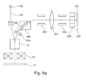
- Fig. 5a shows an embodiment of a secondary charged particle detection system for a charged particle beam device including an energy filtering electrode 200 (or a retarding electrode), arranged between the focusing lens 301 and the detection element 222.
- the energy filtering electrode 200 allows energy filtering of the secondary particle bundle.
- the energy filtering electrode can be a tube or a plate that can be biased to a voltage close to the voltage applied to the specimen.
- the electron beam enters filter 200 provided in form of a cylinder.
- a potential-saddle is applied due to biasing of the cylinder. Electrons having a sufficiently large energy can pass the potential-saddle (potential hill). Other electrons are backwardly redirected. Yet, all electrons are influenced by the same potential-saddle.
- the opening of the cylinder requires a defined sufficiently large size. Thereby, the transparency of the filter is increased. There are no losses due to impingement of electrons on a grid and hardly any losses due to an insufficiently focused beam.
- additional detection elements 224 or sensors can be arranged around an optical axis in the detection system as shown in Fig. 5b .
- the energy filtering detector can include the following features: a divider is provided, e.g. in the form of a filter 200 as described above, to divide the beam of charged particles according to their energies into a low energy beam and a high energy beam.
- the at least one reverse detector and/or the front detector is segmented to provide a spatial resolution of the particles from the incoming beam of charged particles.
- a secondary charged particle detection system for a charged particle beam device further includes a topography detector.
- a topography detector is provided between the focusing lens and the detection element.
- Fig. 6 shows an embodiment of a secondary charged particle detection system for a charged particle beam device including a topography detector 210 with a plate 201, arranged between the focusing lens 301 and the detection element 222.
- a topography detector 210 with a plate 201, arranged between the focusing lens 301 and the detection element 222.
- Topography detectors are usually divided into 4 or more segments (with or without a central BF area) which can be read separately. The signals can then be combined (e.g. subtracted) to enhance contrast.
- an optical system including a beam splitter 15 that separates the primary beam 130 and the SE bundle 140, a beam bender 440 that deflects the SE bundle to a large angle (typically 90° for horizontal exit), SE focus lens 301 and a first, a second and a third alignment deflector for focusing and aligning the beam to the sensor.
- the topography detector 210 allows topographic imaging using multiple separated sensor channels, but can also be switched to BF imaging and energy filtering mode.
- a charged particle beam device including a secondary charged particle detection system.
- the detection system includes a beam splitter for separating a primary beam and a secondary beam formed upon impact on a specimen; a beam bender for deflecting the secondary beam; a focusing lens for focusing the secondary beam; a detection element for detecting the secondary beam particles, and three deflection elements, wherein at least a first deflector is provided between the beam bender and the focusing lens, at least a second deflector is provided between the focusing lens and the detection element, at least a third deflector is provided between the beam splitter and the detection element.
- a secondary charged particle detection device for detection of a signal beam
- the detection device can be part of an SE optics according to embodiments described herein.
- the device includes a detector arrangement having at least two detection elements with active detection areas, wherein the active detection areas are separated by a gap, a particle optics configured for separating the signal beam into a first portion of the signal beam and into at least one second portion of the signal beam, and configured for focusing the first portion of the signal beam and the at least one second portion of the signal beam.
- the particle optics includes an aperture plate and at least a first aperture opening in the aperture plate, and at least one second aperture opening in the aperture plate, wherein the aperture plate is configured to be biased to one potential surrounding the first aperture opening and the at least one second aperture opening.
- the SE particle optics includes at least an aperture plate 201 having two or more aperture openings.
- the aperture plate 201 can be biased to a deceleration potential.
- the deceleration of the aperture plate 201 in combination with an acceleration of the detection elements 222 are configured for a separation and focusing of the secondary particles, e.g. the secondary electron beam.
- the separation of the secondary beam on different detection elements can be provided.
- the aperture plate 201 has a central aperture opening 202 and at least two radially outer aperture openings 204. Typically, four outer aperture openings 204 can be provided.
- a method of detection of secondary charged particles in a charged particle beam device includes separating a secondary beam from a primary beam by means of a beam separator; deflecting the separated secondary beam by means of a main deflector; and focusing the secondary beam on a detection element by means of a focusing lens; wherein the secondary beam is deflected by at least a first deflector provided between the beam bender and the focusing lens, at least a second deflector provided between the focusing lens and the detection element, and at least a third deflector provided between the beam splitter and the detection element.
- Fig. 7 shows a block diagram of a method of detection of charged particles in a charged particle beam device according to embodiments described herein.
- the method includes: separating 101 a secondary beam from a primary beam by means of a beam separator; deflecting 102 the separated secondary beam by means of a main deflector; focusing 103 the secondary beam on a detection element by means of a focusing lens; wherein the focusing of the secondary beam is conducted such that a minimum aberration plane within the main deflector is imaged onto the detection element.
Landscapes
- Chemical & Material Sciences (AREA)
- Analytical Chemistry (AREA)
- Physics & Mathematics (AREA)
- Health & Medical Sciences (AREA)
- Life Sciences & Earth Sciences (AREA)
- Biochemistry (AREA)
- General Health & Medical Sciences (AREA)
- General Physics & Mathematics (AREA)
- Immunology (AREA)
- Pathology (AREA)
- Testing Or Measuring Of Semiconductors Or The Like (AREA)
- Analysing Materials By The Use Of Radiation (AREA)
Priority Applications (6)
| Application Number | Priority Date | Filing Date | Title |
|---|---|---|---|
| EP12198963.6A EP2747121A1 (de) | 2012-12-21 | 2012-12-21 | Sekundärelektronenoptik und -detektionsvorrichtung |
| US13/734,180 US20140175277A1 (en) | 2012-12-21 | 2013-01-04 | Secondary electron optics and detection device |
| TW102147554A TWI603363B (zh) | 2012-12-21 | 2013-12-20 | 二次帶電粒子偵測系統、帶電粒子束裝置及偵測二次帶電粒子的方法 |
| KR1020130160274A KR102207766B1 (ko) | 2012-12-21 | 2013-12-20 | 이차 전자 광학계 & 검출 디바이스 |
| JP2013263448A JP6278553B2 (ja) | 2012-12-21 | 2013-12-20 | 2次電子光学系及び検出デバイス |
| US14/690,063 US20150228452A1 (en) | 2012-12-21 | 2015-04-17 | Secondary electron optics and detection device |
Applications Claiming Priority (1)
| Application Number | Priority Date | Filing Date | Title |
|---|---|---|---|
| EP12198963.6A EP2747121A1 (de) | 2012-12-21 | 2012-12-21 | Sekundärelektronenoptik und -detektionsvorrichtung |
Publications (1)
| Publication Number | Publication Date |
|---|---|
| EP2747121A1 true EP2747121A1 (de) | 2014-06-25 |
Family
ID=47522333
Family Applications (1)
| Application Number | Title | Priority Date | Filing Date |
|---|---|---|---|
| EP12198963.6A Withdrawn EP2747121A1 (de) | 2012-12-21 | 2012-12-21 | Sekundärelektronenoptik und -detektionsvorrichtung |
Country Status (5)
| Country | Link |
|---|---|
| US (2) | US20140175277A1 (de) |
| EP (1) | EP2747121A1 (de) |
| JP (1) | JP6278553B2 (de) |
| KR (1) | KR102207766B1 (de) |
| TW (1) | TWI603363B (de) |
Cited By (2)
| Publication number | Priority date | Publication date | Assignee | Title |
|---|---|---|---|---|
| CN111727489A (zh) * | 2017-12-15 | 2020-09-29 | 德累斯顿莱布尼茨固体材料研究所 | 动量分辨光电子能谱仪及用于动量分辨光电子能谱的方法 |
| TWI818407B (zh) * | 2021-01-21 | 2023-10-11 | 日商紐富來科技股份有限公司 | 多射束圖像取得裝置及多射束圖像取得方法 |
Families Citing this family (13)
| Publication number | Priority date | Publication date | Assignee | Title |
|---|---|---|---|---|
| US9805908B2 (en) * | 2015-02-18 | 2017-10-31 | Integrated Circuit Testing Gesellschaft für Halbleiterprüftechnik mbH | Signal charged particle deflection device, signal charged particle detection system, charged particle beam device and method of detection of a signal charged particle beam |
| JP6701228B2 (ja) * | 2015-03-24 | 2020-05-27 | ケーエルエー コーポレイション | 像ビームの安定化及び識別性が改善された荷電粒子顕微システム及び方法 |
| CN111261481B (zh) * | 2015-03-24 | 2022-12-16 | 科磊股份有限公司 | 用于带电粒子显微镜的方法及系统 |
| US10103004B2 (en) | 2015-07-02 | 2018-10-16 | ICT Integrated Circuit Testing Gesellschaft für Halbleiterprüftechnik mbH | System and method for imaging a secondary charged particle beam with adaptive secondary charged particle optics |
| US10056224B2 (en) * | 2015-08-10 | 2018-08-21 | Kla-Tencor Corporation | Method and system for edge-of-wafer inspection and review |
| DE112016006484B4 (de) * | 2016-03-31 | 2022-02-03 | Hitachi, Ltd. | Ladungsträgerstrahlvorrichtung sowie Steuerverfahren |
| KR102520386B1 (ko) * | 2017-03-20 | 2023-04-11 | 칼 짜이스 마이크로스카피 게엠베하 | 하전 입자 빔 시스템 및 방법 |
| JP6880209B2 (ja) * | 2017-09-29 | 2021-06-02 | 株式会社日立ハイテク | 走査電子顕微鏡 |
| US10770262B1 (en) * | 2018-05-30 | 2020-09-08 | National Technology & Engineering Solutions Of Sandia, Llc | Apparatus, method and system for imaging and utilization of SEM charged particles |
| JP2019215957A (ja) * | 2018-06-11 | 2019-12-19 | 株式会社荏原製作所 | ビームベンダ |
| US11094501B2 (en) * | 2019-11-19 | 2021-08-17 | ICT Integrated Circuit Testing Gesellschaft für Halbleiterprüftechnik mbH | Secondary charged particle imaging system |
| KR102922717B1 (ko) * | 2021-03-26 | 2026-02-05 | 주식회사 히타치하이테크 | 하전 입자빔 시스템 |
| KR20230068893A (ko) * | 2021-11-11 | 2023-05-18 | 삼성전자주식회사 | 주사 전자 현미경(Scannig Electron Microscope, 이하 SEM), SEM을 동작시키는 방법 및 이를 이용한 반도체 소자를 제조하는 방법 |
Citations (6)
| Publication number | Priority date | Publication date | Assignee | Title |
|---|---|---|---|---|
| EP1657736A1 (de) * | 2004-11-15 | 2006-05-17 | ICT Integrated Circuit Testing Gesellschaft für Halbleiterprüftechnik mbH | Elektronenstrahlvorrichtung für hohe Stromdichten |
| EP1703537A1 (de) * | 2005-03-17 | 2006-09-20 | ICT Integrated Circuit Testing Gesellschaft für Halbleiterprüftechnik mbH | Analyse-System und Teilchenstrahlgerät |
| JP2008078058A (ja) * | 2006-09-25 | 2008-04-03 | Ebara Corp | 電子線装置及びこれを用いたパターン評価方法 |
| EP2333808A1 (de) * | 2009-12-11 | 2011-06-15 | ICT Integrated Circuit Testing Gesellschaft für Halbleiterprüftechnik mbH | Vorrichtung mit geladenem Teilchenstrahl, Verfahren zum Betrieb der Vorrichtung mit geladenem Teilchenstrahl |
| EP2654069A1 (de) * | 2012-04-16 | 2013-10-23 | ICT Integrated Circuit Testing Gesellschaft für Halbleiterprüftechnik mbH | Mehrkanaldetektor, Optik dafür und Betriebsverfahren dafür |
| EP2654068A1 (de) * | 2012-04-16 | 2013-10-23 | ICT Integrated Circuit Testing Gesellschaft für Halbleiterprüftechnik mbH | Umschaltbarer Mehrperspektivendetektor, Optik dafür und Betriebsverfahren dafür |
Family Cites Families (11)
| Publication number | Priority date | Publication date | Assignee | Title |
|---|---|---|---|---|
| JPS6030415U (ja) * | 1983-08-05 | 1985-03-01 | 石川光学工業株式会社 | 光学装置 |
| JP3518271B2 (ja) * | 1997-08-28 | 2004-04-12 | 株式会社日立製作所 | エネルギーフィルタおよびこれを備えた電子顕微鏡 |
| JP3441955B2 (ja) * | 1998-02-23 | 2003-09-02 | 株式会社日立製作所 | 投射方式の荷電粒子顕微鏡および基板検査システム |
| US6407373B1 (en) * | 1999-06-15 | 2002-06-18 | Applied Materials, Inc. | Apparatus and method for reviewing defects on an object |
| EP1489641B1 (de) * | 2003-06-18 | 2019-08-14 | ICT Integrated Circuit Testing Gesellschaft für Halbleiterprüftechnik mbH | Ablenksystem für geladene Teilchen |
| US7235799B2 (en) * | 2003-11-28 | 2007-06-26 | Ebara Corporation | System and method for evaluation using electron beam and manufacture of devices |
| US20070228922A1 (en) * | 2006-03-29 | 2007-10-04 | Mamora Nakasuji | Electron gun and electron beam apparatus field of invention |
| TWI485742B (zh) * | 2006-09-12 | 2015-05-21 | 荏原製作所股份有限公司 | 荷電粒子束裝置及使用該裝置之半導體元件製造方法 |
| US7759642B2 (en) * | 2008-04-30 | 2010-07-20 | Applied Materials Israel, Ltd. | Pattern invariant focusing of a charged particle beam |
| US8432441B2 (en) * | 2011-02-22 | 2013-04-30 | Hermes Microvision Inc. | Method and system for measuring critical dimension and monitoring fabrication uniformity |
| US9111715B2 (en) * | 2011-11-08 | 2015-08-18 | Fei Company | Charged particle energy filter |
-
2012
- 2012-12-21 EP EP12198963.6A patent/EP2747121A1/de not_active Withdrawn
-
2013
- 2013-01-04 US US13/734,180 patent/US20140175277A1/en not_active Abandoned
- 2013-12-20 KR KR1020130160274A patent/KR102207766B1/ko active Active
- 2013-12-20 JP JP2013263448A patent/JP6278553B2/ja active Active
- 2013-12-20 TW TW102147554A patent/TWI603363B/zh not_active IP Right Cessation
-
2015
- 2015-04-17 US US14/690,063 patent/US20150228452A1/en not_active Abandoned
Patent Citations (6)
| Publication number | Priority date | Publication date | Assignee | Title |
|---|---|---|---|---|
| EP1657736A1 (de) * | 2004-11-15 | 2006-05-17 | ICT Integrated Circuit Testing Gesellschaft für Halbleiterprüftechnik mbH | Elektronenstrahlvorrichtung für hohe Stromdichten |
| EP1703537A1 (de) * | 2005-03-17 | 2006-09-20 | ICT Integrated Circuit Testing Gesellschaft für Halbleiterprüftechnik mbH | Analyse-System und Teilchenstrahlgerät |
| JP2008078058A (ja) * | 2006-09-25 | 2008-04-03 | Ebara Corp | 電子線装置及びこれを用いたパターン評価方法 |
| EP2333808A1 (de) * | 2009-12-11 | 2011-06-15 | ICT Integrated Circuit Testing Gesellschaft für Halbleiterprüftechnik mbH | Vorrichtung mit geladenem Teilchenstrahl, Verfahren zum Betrieb der Vorrichtung mit geladenem Teilchenstrahl |
| EP2654069A1 (de) * | 2012-04-16 | 2013-10-23 | ICT Integrated Circuit Testing Gesellschaft für Halbleiterprüftechnik mbH | Mehrkanaldetektor, Optik dafür und Betriebsverfahren dafür |
| EP2654068A1 (de) * | 2012-04-16 | 2013-10-23 | ICT Integrated Circuit Testing Gesellschaft für Halbleiterprüftechnik mbH | Umschaltbarer Mehrperspektivendetektor, Optik dafür und Betriebsverfahren dafür |
Cited By (3)
| Publication number | Priority date | Publication date | Assignee | Title |
|---|---|---|---|---|
| CN111727489A (zh) * | 2017-12-15 | 2020-09-29 | 德累斯顿莱布尼茨固体材料研究所 | 动量分辨光电子能谱仪及用于动量分辨光电子能谱的方法 |
| CN111727489B (zh) * | 2017-12-15 | 2023-11-17 | 德累斯顿莱布尼茨固体材料研究所 | 动量分辨光电子能谱仪及用于动量分辨光电子能谱的方法 |
| TWI818407B (zh) * | 2021-01-21 | 2023-10-11 | 日商紐富來科技股份有限公司 | 多射束圖像取得裝置及多射束圖像取得方法 |
Also Published As
| Publication number | Publication date |
|---|---|
| US20140175277A1 (en) | 2014-06-26 |
| JP6278553B2 (ja) | 2018-02-14 |
| TWI603363B (zh) | 2017-10-21 |
| US20150228452A1 (en) | 2015-08-13 |
| JP2014123565A (ja) | 2014-07-03 |
| KR20140081728A (ko) | 2014-07-01 |
| TW201426810A (zh) | 2014-07-01 |
| KR102207766B1 (ko) | 2021-01-26 |
Similar Documents
| Publication | Publication Date | Title |
|---|---|---|
| EP2747121A1 (de) | Sekundärelektronenoptik und -detektionsvorrichtung | |
| TWI650550B (zh) | 用於高產量電子束檢測(ebi)的多射束裝置 | |
| JP6641011B2 (ja) | 複数の荷電粒子ビームの装置 | |
| US9922796B1 (en) | Method for inspecting a specimen and charged particle multi-beam device | |
| US9953805B2 (en) | System for imaging a secondary charged particle beam with adaptive secondary charged particle optics | |
| KR20200051560A (ko) | 1차 하전 입자 빔렛들의 어레이를 이용한 시료의 검사를 위한 하전 입자 빔 디바이스 | |
| EP2511939B1 (de) | Anordnung und Verfahren zur Kontrastverbesserung in einem Teilchenstrahlapparat zur Inspektion eines Probestücks | |
| US9305740B2 (en) | Charged particle beam system and method of operating thereof | |
| TW201833968A (zh) | 用於檢查試樣之方法以及帶電粒子多束裝置 | |
| TWI523064B (zh) | 可切換式多視角偵測器與用於其之光學器件及其操作方法 | |
| EP2219204B1 (de) | Anordnung und Verfahren zur Kontrastverbesserung in einer Vorrichtung mit geladenem Partikelstrahl zur Inspektion eines Probestücks | |
| US10297418B2 (en) | Method of reducing coma and chromatic aberration in a charged particle beam device, and charged particle beam device | |
| EP1883094B1 (de) | Teilchenstrahlapparat und Verfahren zur Untersuchung einer Probe |
Legal Events
| Date | Code | Title | Description |
|---|---|---|---|
| PUAI | Public reference made under article 153(3) epc to a published international application that has entered the european phase |
Free format text: ORIGINAL CODE: 0009012 |
|
| 17P | Request for examination filed |
Effective date: 20121221 |
|
| AK | Designated contracting states |
Kind code of ref document: A1 Designated state(s): AL AT BE BG CH CY CZ DE DK EE ES FI FR GB GR HR HU IE IS IT LI LT LU LV MC MK MT NL NO PL PT RO RS SE SI SK SM TR |
|
| AX | Request for extension of the european patent |
Extension state: BA ME |
|
| R17P | Request for examination filed (corrected) |
Effective date: 20141223 |
|
| RBV | Designated contracting states (corrected) |
Designated state(s): AL AT BE BG CH CY CZ DE DK EE ES FI FR GB GR HR HU IE IS IT LI LT LU LV MC MK MT NL NO PL PT RO RS SE SI SK SM TR |
|
| 17Q | First examination report despatched |
Effective date: 20160726 |
|
| STAA | Information on the status of an ep patent application or granted ep patent |
Free format text: STATUS: THE APPLICATION IS DEEMED TO BE WITHDRAWN |
|
| 18D | Application deemed to be withdrawn |
Effective date: 20170207 |