EP2747268B1 - Convertisseur de puissance source de tension, multiniveaux, controlè en courant - Google Patents
Convertisseur de puissance source de tension, multiniveaux, controlè en courant Download PDFInfo
- Publication number
- EP2747268B1 EP2747268B1 EP13196286.2A EP13196286A EP2747268B1 EP 2747268 B1 EP2747268 B1 EP 2747268B1 EP 13196286 A EP13196286 A EP 13196286A EP 2747268 B1 EP2747268 B1 EP 2747268B1
- Authority
- EP
- European Patent Office
- Prior art keywords
- conductive path
- electrically coupled
- power converter
- node
- power
- Prior art date
- Legal status (The legal status is an assumption and is not a legal conclusion. Google has not performed a legal analysis and makes no representation as to the accuracy of the status listed.)
- Active
Links
Images




Classifications
-
- H—ELECTRICITY
- H02—GENERATION; CONVERSION OR DISTRIBUTION OF ELECTRIC POWER
- H02M—APPARATUS FOR CONVERSION BETWEEN AC AND AC, BETWEEN AC AND DC, OR BETWEEN DC AND DC, AND FOR USE WITH MAINS OR SIMILAR POWER SUPPLY SYSTEMS; CONVERSION OF DC OR AC INPUT POWER INTO SURGE OUTPUT POWER; CONTROL OR REGULATION THEREOF
- H02M3/00—Conversion of DC power input into DC power output
- H02M3/02—Conversion of DC power input into DC power output without intermediate conversion into AC
- H02M3/04—Conversion of DC power input into DC power output without intermediate conversion into AC by static converters
- H02M3/06—Conversion of DC power input into DC power output without intermediate conversion into AC by static converters using resistors or capacitors, e.g. potential divider
- H02M3/07—Conversion of DC power input into DC power output without intermediate conversion into AC by static converters using resistors or capacitors, e.g. potential divider using capacitors charged and discharged alternately by semiconductor devices with control electrode, e.g. charge pumps
-
- H—ELECTRICITY
- H02—GENERATION; CONVERSION OR DISTRIBUTION OF ELECTRIC POWER
- H02M—APPARATUS FOR CONVERSION BETWEEN AC AND AC, BETWEEN AC AND DC, OR BETWEEN DC AND DC, AND FOR USE WITH MAINS OR SIMILAR POWER SUPPLY SYSTEMS; CONVERSION OF DC OR AC INPUT POWER INTO SURGE OUTPUT POWER; CONTROL OR REGULATION THEREOF
- H02M1/00—Details of apparatus for conversion
- H02M1/0095—Hybrid converter topologies, e.g. NPC mixed with flying capacitor, thyristor converter mixed with MMC or charge pump mixed with buck
-
- H—ELECTRICITY
- H02—GENERATION; CONVERSION OR DISTRIBUTION OF ELECTRIC POWER
- H02M—APPARATUS FOR CONVERSION BETWEEN AC AND AC, BETWEEN AC AND DC, OR BETWEEN DC AND DC, AND FOR USE WITH MAINS OR SIMILAR POWER SUPPLY SYSTEMS; CONVERSION OF DC OR AC INPUT POWER INTO SURGE OUTPUT POWER; CONTROL OR REGULATION THEREOF
- H02M3/00—Conversion of DC power input into DC power output
- H02M3/02—Conversion of DC power input into DC power output without intermediate conversion into AC
- H02M3/04—Conversion of DC power input into DC power output without intermediate conversion into AC by static converters
- H02M3/10—Conversion of DC power input into DC power output without intermediate conversion into AC by static converters using discharge tubes with control electrode or semiconductor devices with control electrode
- H02M3/145—Conversion of DC power input into DC power output without intermediate conversion into AC by static converters using discharge tubes with control electrode or semiconductor devices with control electrode using devices of a triode or transistor type requiring continuous application of a control signal
- H02M3/155—Conversion of DC power input into DC power output without intermediate conversion into AC by static converters using discharge tubes with control electrode or semiconductor devices with control electrode using devices of a triode or transistor type requiring continuous application of a control signal using semiconductor devices only
- H02M3/156—Conversion of DC power input into DC power output without intermediate conversion into AC by static converters using discharge tubes with control electrode or semiconductor devices with control electrode using devices of a triode or transistor type requiring continuous application of a control signal using semiconductor devices only with automatic control of output voltage or current, e.g. switching regulators
- H02M3/158—Conversion of DC power input into DC power output without intermediate conversion into AC by static converters using discharge tubes with control electrode or semiconductor devices with control electrode using devices of a triode or transistor type requiring continuous application of a control signal using semiconductor devices only with automatic control of output voltage or current, e.g. switching regulators including plural semiconductor devices as final control devices for a single load
-
- H—ELECTRICITY
- H02—GENERATION; CONVERSION OR DISTRIBUTION OF ELECTRIC POWER
- H02M—APPARATUS FOR CONVERSION BETWEEN AC AND AC, BETWEEN AC AND DC, OR BETWEEN DC AND DC, AND FOR USE WITH MAINS OR SIMILAR POWER SUPPLY SYSTEMS; CONVERSION OF DC OR AC INPUT POWER INTO SURGE OUTPUT POWER; CONTROL OR REGULATION THEREOF
- H02M5/00—Conversion of AC power input into AC power output, e.g. for change of voltage, for change of frequency, for change of number of phases
- H02M5/40—Conversion of AC power input into AC power output, e.g. for change of voltage, for change of frequency, for change of number of phases with intermediate conversion into DC
- H02M5/42—Conversion of AC power input into AC power output, e.g. for change of voltage, for change of frequency, for change of number of phases with intermediate conversion into DC by static converters
- H02M5/44—Conversion of AC power input into AC power output, e.g. for change of voltage, for change of frequency, for change of number of phases with intermediate conversion into DC by static converters using discharge tubes or semiconductor devices to convert the intermediate DC into AC
- H02M5/453—Conversion of AC power input into AC power output, e.g. for change of voltage, for change of frequency, for change of number of phases with intermediate conversion into DC by static converters using discharge tubes or semiconductor devices to convert the intermediate DC into AC using devices of a triode or transistor type requiring continuous application of a control signal
- H02M5/458—Conversion of AC power input into AC power output, e.g. for change of voltage, for change of frequency, for change of number of phases with intermediate conversion into DC by static converters using discharge tubes or semiconductor devices to convert the intermediate DC into AC using devices of a triode or transistor type requiring continuous application of a control signal using semiconductor devices only
-
- H—ELECTRICITY
- H02—GENERATION; CONVERSION OR DISTRIBUTION OF ELECTRIC POWER
- H02M—APPARATUS FOR CONVERSION BETWEEN AC AND AC, BETWEEN AC AND DC, OR BETWEEN DC AND DC, AND FOR USE WITH MAINS OR SIMILAR POWER SUPPLY SYSTEMS; CONVERSION OF DC OR AC INPUT POWER INTO SURGE OUTPUT POWER; CONTROL OR REGULATION THEREOF
- H02M7/00—Conversion of AC power input into DC power output; Conversion of DC power input into AC power output
- H02M7/02—Conversion of AC power input into DC power output without possibility of reversal
- H02M7/04—Conversion of AC power input into DC power output without possibility of reversal by static converters
- H02M7/12—Conversion of AC power input into DC power output without possibility of reversal by static converters using discharge tubes with control electrode or semiconductor devices with control electrode
- H02M7/21—Conversion of AC power input into DC power output without possibility of reversal by static converters using discharge tubes with control electrode or semiconductor devices with control electrode using devices of a triode or transistor type requiring continuous application of a control signal
- H02M7/217—Conversion of AC power input into DC power output without possibility of reversal by static converters using discharge tubes with control electrode or semiconductor devices with control electrode using devices of a triode or transistor type requiring continuous application of a control signal using semiconductor devices only
-
- H—ELECTRICITY
- H02—GENERATION; CONVERSION OR DISTRIBUTION OF ELECTRIC POWER
- H02M—APPARATUS FOR CONVERSION BETWEEN AC AND AC, BETWEEN AC AND DC, OR BETWEEN DC AND DC, AND FOR USE WITH MAINS OR SIMILAR POWER SUPPLY SYSTEMS; CONVERSION OF DC OR AC INPUT POWER INTO SURGE OUTPUT POWER; CONTROL OR REGULATION THEREOF
- H02M7/00—Conversion of AC power input into DC power output; Conversion of DC power input into AC power output
- H02M7/42—Conversion of DC power input into AC power output without possibility of reversal
- H02M7/44—Conversion of DC power input into AC power output without possibility of reversal by static converters
- H02M7/48—Conversion of DC power input into AC power output without possibility of reversal by static converters using discharge tubes with control electrode or semiconductor devices with control electrode
- H02M7/483—Converters with outputs that each can have more than two voltages levels
-
- H—ELECTRICITY
- H02—GENERATION; CONVERSION OR DISTRIBUTION OF ELECTRIC POWER
- H02M—APPARATUS FOR CONVERSION BETWEEN AC AND AC, BETWEEN AC AND DC, OR BETWEEN DC AND DC, AND FOR USE WITH MAINS OR SIMILAR POWER SUPPLY SYSTEMS; CONVERSION OF DC OR AC INPUT POWER INTO SURGE OUTPUT POWER; CONTROL OR REGULATION THEREOF
- H02M7/00—Conversion of AC power input into DC power output; Conversion of DC power input into AC power output
- H02M7/42—Conversion of DC power input into AC power output without possibility of reversal
- H02M7/44—Conversion of DC power input into AC power output without possibility of reversal by static converters
- H02M7/48—Conversion of DC power input into AC power output without possibility of reversal by static converters using discharge tubes with control electrode or semiconductor devices with control electrode
- H02M7/483—Converters with outputs that each can have more than two voltages levels
- H02M7/4835—Converters with outputs that each can have more than two voltages levels comprising two or more cells, each including a switchable capacitor, the capacitors having a nominal charge voltage which corresponds to a given fraction of the input voltage, and the capacitors being selectively connected in series to determine the instantaneous output voltage
-
- H—ELECTRICITY
- H02—GENERATION; CONVERSION OR DISTRIBUTION OF ELECTRIC POWER
- H02M—APPARATUS FOR CONVERSION BETWEEN AC AND AC, BETWEEN AC AND DC, OR BETWEEN DC AND DC, AND FOR USE WITH MAINS OR SIMILAR POWER SUPPLY SYSTEMS; CONVERSION OF DC OR AC INPUT POWER INTO SURGE OUTPUT POWER; CONTROL OR REGULATION THEREOF
- H02M7/00—Conversion of AC power input into DC power output; Conversion of DC power input into AC power output
- H02M7/42—Conversion of DC power input into AC power output without possibility of reversal
- H02M7/44—Conversion of DC power input into AC power output without possibility of reversal by static converters
- H02M7/48—Conversion of DC power input into AC power output without possibility of reversal by static converters using discharge tubes with control electrode or semiconductor devices with control electrode
- H02M7/483—Converters with outputs that each can have more than two voltages levels
- H02M7/4837—Flying capacitor converters
-
- H—ELECTRICITY
- H02—GENERATION; CONVERSION OR DISTRIBUTION OF ELECTRIC POWER
- H02M—APPARATUS FOR CONVERSION BETWEEN AC AND AC, BETWEEN AC AND DC, OR BETWEEN DC AND DC, AND FOR USE WITH MAINS OR SIMILAR POWER SUPPLY SYSTEMS; CONVERSION OF DC OR AC INPUT POWER INTO SURGE OUTPUT POWER; CONTROL OR REGULATION THEREOF
- H02M1/00—Details of apparatus for conversion
- H02M1/0083—Converters characterised by their input or output configuration
- H02M1/0085—Partially controlled bridges
-
- H—ELECTRICITY
- H02—GENERATION; CONVERSION OR DISTRIBUTION OF ELECTRIC POWER
- H02M—APPARATUS FOR CONVERSION BETWEEN AC AND AC, BETWEEN AC AND DC, OR BETWEEN DC AND DC, AND FOR USE WITH MAINS OR SIMILAR POWER SUPPLY SYSTEMS; CONVERSION OF DC OR AC INPUT POWER INTO SURGE OUTPUT POWER; CONTROL OR REGULATION THEREOF
- H02M7/00—Conversion of AC power input into DC power output; Conversion of DC power input into AC power output
- H02M7/42—Conversion of DC power input into AC power output without possibility of reversal
- H02M7/44—Conversion of DC power input into AC power output without possibility of reversal by static converters
- H02M7/48—Conversion of DC power input into AC power output without possibility of reversal by static converters using discharge tubes with control electrode or semiconductor devices with control electrode
- H02M7/483—Converters with outputs that each can have more than two voltages levels
- H02M7/487—Neutral point clamped inverters
Definitions
- Embodiments of the invention generally relate to power converters and more particularly to multilevel power converters.
- alternating current (AC) transmission systems have been used for high voltage power transmission, however, the AC transmission systems suffer from undesired cable capacitance that results in charging current requirements.
- high voltage direct current (HVDC) transmission provides a more efficient way to transmit high voltage power over long distances.
- power converters are often used to convert AC power to DC power at the transmitting substation and to convert the transmitted DC power back to AC power at the receiving substation.
- these power converters have a modular multilevel structure where each phase has a stacked arrangement of modules.
- Each of the modules comprises an AC-DC power converter that converts a fraction of the AC power to the DC power at the transmitting substation.
- the modular AC-DC power converters include voltage source power converters which are coupled to each other to form a modular stacked multilevel power converter that supports a unidirectional DC current flow.
- two level and three level voltage source modular power converters are used which results in a high number of modules being coupled together to form the modular stacked power converter with a desired AC-DC power conversion capability. Higher numbers of modules results in complexity and high costs.
- WO 2011/124260 describes a modularized voltage source converter for HVDC and STATCOM including at least one chain-link converter with a chain of modules connected in series.
- WO 2011/100738 describes multilevel inverters with bidirectional switching interconnections.
- EP 0891037 describes a method of combining voltage pulses of first and second converters with first and second degrees of modulation so that a common voltage pulse without gaps is produced.
- US 2012/0063185 describes a modular switch for a converter.
- US 2005/083716 describes a power supply with a direct converter.
- WO 2011/124258 describes a hybrid HVDC converter.
- Embodiments of the present invention include a power converter module that comprises a voltage source current controlled power converter which provides unidirectional current and has at least four output voltage levels.
- the voltage source current controlled power converter includes an input terminal that receives modular input current and an output terminal that provides modular output current.
- the voltage source current controlled power converter also includes a first conductive path and a second conductive path coupled in parallel to each other between the input terminal and the output terminal, wherein each of the conductive paths comprises at least one diode coupled in series to the respective conductive path.
- the at least one diode in the first conductive path is coupled closer to the input terminal than the output terminal, and the at least one diode in the second conductive path is coupled closer to the output terminal than the input terminal.
- the voltage source current controlled power converter further includes energy storage elements coupled between the first conductive path and the second conductive path.
- module input current is defined as the input current that is received by one power converter module
- modular output current is defined as the output current that is provided by one power converter module.
- system input power is defined as the input power received by the AC-DC power conversion system including the power converter modules.
- system output power is defined as the output power that is provided by the AC-DC power conversion system.
- circuit circuitry
- controller processor
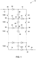
- FIG. 1 is a schematic representation of a voltage source current controlled power converter 10 including N voltage levels in a diode clamped configuration in accordance with an embodiment of the invention.
- the voltage source current controlled power converter 10 includes an input terminal 12 that is coupled to a power source (not shown) and receives a modular input current from the power source.
- the voltage source current controlled power converter 10 further includes an output terminal 14 that provides a modular output current.
- the voltage source current controlled power converter 10 includes a first conductive path 16 and a second conductive path 18 coupled in parallel to each other. The first conductive path 16 and the second conductive path 18 are coupled to the input terminal 12 at a first end 20 and to the output terminal 14 at a second end 22.
- Each of the first conductive path 16 and the second conductive path 18 includes at least one diode 24, 1024 coupled in series to the respective conductive paths wherein the at least one diode 24 of the first conductive path 16 is coupled closer to the input terminal 12 than the output terminal 14 and the at least one diode 1024 of the second conductive path 18 is coupled closer to the output terminal 14 than the input terminal 12.
- the voltage source current controlled power converter 10 also includes energy storage elements 28 coupled between the first conductive path 16 and the second conductive path 18.
- the energy storage element 28 includes a capacitor.
- the voltage source current controlled power converter 10 includes switches 30, 1030 in the first conductive path 16 and the second conductive path 18 wherein the switches 30, 1030 in the respective conductive paths 16, 18 are coupled in series to each other.
- the switches 30, 1030 comprise unidirectional current switches.
- the switches 30, 1030 comprise thyristors, insulated gate bipolar transistors (IGBT) or integrated gate-commutated thyristors (IGCT).
- the voltage source current controlled power converter 10 includes converter legs 32 coupled between the first conductive path 16 and the second conductive path 18 wherein each converter leg 32 is coupled between a respective pair of switches 30 in the first conductive path 16 at a first node 34 and between a corresponding pair of switches 1030 in the second conductive path 18 at a second node 36. Further, each of the converter leg 32 is coupled between a respective pair of energy storage elements 28 at an intermediate node 38, and each converter leg 32 includes two leg diodes 40 coupled in series to each other such that the intermediate node 38 is positioned between the two leg diodes 40.
- the number of switches 30, 1030, the number of converter legs 32, and the number of energy storage elements 28 for the voltage source current controlled power converter 10 is determined based on a number of voltage levels that is required between the input terminal 12 and the output terminal 14.
- FIG. 2 is a schematic representation of a voltage source current controlled power converter 100 including N voltage levels in an actively clamped configuration in accordance with an embodiment of the invention.
- the voltage source current controlled power converter 100 includes an actively clamped configuration which includes the first conductive path 116 and the second conductive path 118 coupled in parallel to each other, and the first conductive path 116 and the second conductive path 118 are coupled to the input terminal 112 at the first end 120 and to the output terminal 114 at the second end 122.
- Each of the conductive paths 116, 118 includes at least one diode 124, 1124 coupled in series to the respective conductive paths and at least one switch 130, 1130 coupled in series to the respective conductive paths.
- the voltage source current controlled power converter 100 also includes energy storage elements 128 coupled between the first conductive path 116 and the second conductive path 118.
- the voltage source current controlled power converter 100 includes converter legs 132 coupled between the first conductive path 116 and the second conductive path 118 at the first node 134 and the second node 136 respectively wherein each converter leg 132 is coupled between a respective pair of energy storage elements 128 at an intermediate node 138.
- Each converter leg 132 includes at least one leg switch 144, at least one leg diode 142 or a combination thereof on both sides of the intermediate node 138.
- the converter leg 132 includes a leg switch 142 and a leg diode 144 on both sides of the intermediate node 138.
- each converter leg 132 may include a switching device that provides the same reverse blocking capabilities as provided by the leg switch 142 and the leg diode 144 on both sides of the intermediate node 138.
- the number of converter legs 132 and the number of energy storage elements 128 for the actively clamped configuration of the voltage source current controlled power converter 100 is determined based on a number of voltage levels that is required between the input terminal 112 and the output terminal 114.
- FIG. 3 is a schematic representation of a voltage source current controlled power converter 200 including N voltage levels in a floating capacitor configuration in accordance with an embodiment of the invention.
- the voltage source current controlled power converter 200 includes a floating capacitor configuration which includes the first conductive path 216 and the second conductive path 218 coupled in parallel to each other and the first conductive path 216 and the second conductive path 218 are coupled to the input terminal 212 at the first end 220 and to the output terminal 214 at the second end 222.
- Each of the conductive paths 216, 218 includes at least one diode 224, 2224 coupled in series to the respective conductive paths.
- the first conductive path 216 includes a plurality of first switching elements (FSE) 2000
- the second conductive path 218 includes a plurality of second switching elements (SSE) 2200.
- the first switching elements 2000 and the second switching elements 2200 may include unidirectional switches and/or additional diodes depending on capacitor voltages of the voltage source current controlled power converter.
- the capacitors 228 are coupled between a respective pair of the first switching elements 2000 at a first capacitor node 246 and between a respective pair of the second switching elements 2200 at a second capacitor node 248.
- the first capacitor node 246 is coupled to the first conductive path 216 and the second capacitor node 248 is coupled to the second conductive path 218.
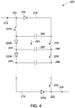
- FIG. 4 is a schematic representation of one specific embodiment of a floating capacitor configuration of the power converter 200 including switches 230 in the first conductive path 216 and diodes 2235 in the second conductive path 218 in accordance with an embodiment of the invention.
- the voltage of a first capacitor 225 is greater than the voltage of a second capacitor 227 as represented by arrow 221
- the plurality of first switching elements 2000 (shown in FIG. 3 ) in the first conductive path 216 include unidirectional switches 230 coupled in series to each other
- the plurality of second switching elements 2200 (shown in FIG. 3 ) in the second conductive path 218 includes diodes 2235 coupled in series to each other.
- FIG. 5 is a schematic representation of another embodiment of a floating capacitor configuration of the power converter 200 including switches 2230 in the second conductive path 218 and diodes 235 in the first conductive path 216 in accordance with an embodiment of the invention.
- the voltage of a first capacitor 225 is lower than the voltage of a second capacitor 227 as represented by arrow 223, and the plurality of first switching elements 2000 ( FIG. 3 ) in the first conductive path 216 includes diodes 235 coupled in series to each other, and the plurality of second switching elements 2200 (shown in FIG. 3 ) in the second conductive path 218 includes unidirectional switches 2230 coupled in series to each other.
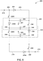
- FIG. 6 is a schematic representation of yet another embodiment of a floating capacitor configuration of the power converter 200 including switches 230, 2230 and diodes 224, 235, 2224, 2235 in the first conductive path 216 and the second conductive path 218 in accordance with an embodiment of the invention.
- the first capacitor 225 and the second capacitor 227 form a first cell 231
- the second capacitor 227 and a third capacitor 229 forms a second cell 233.
- the first switching elements 2000 shown in FIG. 3
- the second switching element 2200 shown in FIG.
- the second conductive path 218 will include a diode 2235 in the first cell 231.
- the first switching element 2000 in the first conductive path 216 of the second cell 233 will include the diode 235 and the second switching element 2200 in the second conductive path 218 of the second cell 233 will include the unidirectional switch 2230. The process is repeated for M number of cells for providing N levels of voltage based on the voltages in the two capacitors in one cell.
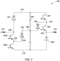
- FIG. 7 is a schematic representation of an exemplary voltage source current controlled power converter 300 including five voltage levels in a diode clamped configuration in accordance with an embodiment of the invention.
- the voltage source current controlled power converter 300 includes a diode clamped configuration which includes the first conductive path 316 and the second conductive path 318 coupled in parallel to each other, and the first conductive path 316 and the second conductive path 318 are coupled to the input terminal 312 at the first end 320 and to the output terminal 314 at the second end 322.
- Each of the conductive paths 316, 318 includes one diode 324, 3324 coupled in series to the respective conductive paths.
- the voltage source current controlled power converter 300 also includes two energy storage elements 328 coupled between the first conductive path 316 and the second conductive path 318.
- the voltage source current controlled power converter 300 includes two switches 330 in the first conductive path 316 and two switches 3330 in the second conductive path 318.
- the voltage source current controlled power converter 300 includes a converter leg 332 coupled between the switches 330 of the first conductive path 316 at the first node 334 and the switches 3330 of the second conductive path 318 at the second node 336.
- the converter leg 332 is coupled between the two energy storage elements 328 at an intermediate node 338, and the converter leg 332 includes two leg diodes 340 coupled in series to each other such that the intermediate node 338 is positioned between the two leg diodes 340.
- FIG. 8 is a schematic representation of a voltage source current controlled power converter 400 including five voltage levels in an actively clamped configuration in accordance with an embodiment of the invention.
- the voltage source current controlled power converter 400 includes an actively clamped configuration which includes the first conductive path 416 and the second conductive path 418 coupled in parallel to each other, and the first conductive path 416 and the second conductive path 418 are coupled to the input terminal 412 at the first end 420 and to the output terminal 414 at the second end 422.
- Each of the conductive paths 416, 418 includes one diode 424, 4424 coupled in series to the respective conductive paths.
- the voltage source current controlled power converter 400 also includes two energy storage elements 428 coupled between the first conductive path 416 and the second conductive path 418.
- the voltage source current controlled power converter 400 includes a converter leg 432 coupled between the first conductive path 416 and the second conductive path 418 at the first node and the second node respectively which coincide with the first end 420 and the second end 422.
- the converter leg 432 is coupled between the two energy storage elements 428 at an intermediate node 438 and includes a leg switch 442 and a leg diode 444 on both sides of the intermediate node 438.
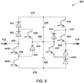
- FIG. 9 is a schematic representation of an alternative embodiment of a voltage source current controlled power converter 450 including five voltage levels in an actively clamped configuration in accordance with an embodiment of the invention.
- the voltage source current controlled power converter 450 includes the converter leg 432 which is coupled between the two energy storage elements 428 at the intermediate node 438, and the converter leg 432 includes a leg switch 442 and a leg diode 444 on both sides of the intermediate node 438 wherein the leg switch 442 and the leg diode 444 on each side of the intermediate node 438 are coupled in series to each other.
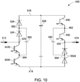
- FIG. 10 is a schematic representation of a voltage source current controlled power converter 500 including five voltage levels in a floating capacitor configuration in accordance with an embodiment of the invention.
- the voltage source current controlled power converter 500 includes a floating capacitor configuration which includes the first conductive path 516 and the second conductive path 518 coupled in parallel to each other and the first conductive path 516 and the second conductive path 518 are coupled to the input terminal 512 at the first end 520 and to the output terminal 514 at the second end 522.
- Each of the conductive paths 516, 518 includes two diodes 524, 5524 coupled in series to the respective conductive paths.
- Each of the conductive paths 516, 518 includes two switches 530, 5530 coupled in series to the respective conductive paths and two capacitors 528 are coupled between the first conductive path 516 and the second conductive path 518.
- a first capacitor 550 is coupled between the two diodes 524 of the first conductive path 516 at the first capacitor node 552 and between the two switches 5530 of the second conductive path 518 at the second capacitor node 554.
- the voltage source current controlled power converter 500 also includes a second capacitor 560 coupled between the switches 530 of the first conductive path 516 at the first capacitor node 562 and between the two diodes 5524 of the second conductive path 518 at the second capacitor node 564.
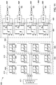
- FIG. 11 is a schematic representation of a modular AC-DC power conversion system 600 including power converter modules 605 coupled to each other for converting AC power to DC power in accordance with an embodiment of the invention.
- the AC-DC power conversion system 600 includes a three phase input power source 611 configured to provide system input power to three phase sets 613, 615, 617 of the power converter modules 605 which are coupled in series to each other, and each phase set 613, 615, 617 converts one phase of the system input power to a system output power.
- the number of power converter modules 605 which are coupled in series for one phase is dependent on the power rating and voltage ratings of the AC-DC power conversion system 600 and may include N number of power converter modules 605 coupled together in series.
- Each of the power converter modules 605 includes a voltage source current controlled power converter for providing unidirectional current having at least four output voltage levels and may include diode clamped configuration, actively clamped configuration, floating capacitor configuration, any variations of the aforementioned configurations or a combination thereof.
- the output terminals 614 of the voltage source current controlled power converter modules 605 are coupled together and the modular output power is transmitted to a receiver end 620 via a DC link 622.
- Receiver end power converter modules 624 may include any of the aforementioned configurations but are used in a different way as compared to the voltage source current controlled power converter modules 605.
- the receiver end power converter modules 624 are coupled to individual loads 626 such as motors, and the first conductive path and the second conductive path of the receiver end power converter module 624 are configured to operate as a DC link to provide the modular output power to the individual loads 626. Moreover, the receiver end power converter modules 624 are configured to provide the same modular output power level when two or more receiver end power converter modules 624 are coupled together. The receiver end power converter modules 624 provide the received modular output power according to the individual load 626 requirements. Each of the receiver end converter modules 624 is coupled to an additional power converter 628 via a DC port where the additional power converter 628 converts the required modular output power received from the receiver end power converter module 624 to the system output power which is used to operate the load 626 at the receiver end 620.
Landscapes
- Engineering & Computer Science (AREA)
- Power Engineering (AREA)
- Inverter Devices (AREA)
- Rectifiers (AREA)
- Direct Current Feeding And Distribution (AREA)
Claims (5)
- Module de convertisseur de puissance comprenant :un convertisseur de puissance commandé par le courant d'une source de tension (10 ; 300) fournissant un courant unidirectionnel avec (2n+1) niveaux de tension de sortie, avec n ≥ 2, le convertisseur de puissance comprenant :une borne d'entrée (12 ; 312) destinée à recevoir un courant d'entrée modulaire ;une borne de sortie (14; 314) destinée à fournir un courant de sortie modulaire ;un premier chemin conducteur (16; 316) et un deuxième chemin conducteur (18; 318) couplés électriquement en parallèle entre eux entre la borne d'entrée (12 ; 312) et la borne de sortie (14 ; 314), dans lequel chacun des premier et deuxième chemins conducteurs (16, 18 ; 316, 318) comprend une diode (24, 1024; 324, 3324) et n interrupteurs (30, 1030 ; 330, 3330) couplés électriquement en série ;dans lequel les n interrupteurs (30 ; 330) du premier chemin conducteur (16 ; 316) sont couplés électriquement par (n-1) premiers noeuds (34; 334) et les n interrupteurs (1030 ; 3330) du deuxième chemin conducteur (18 ; 318) sont couplés électriquement par (n-1) deuxièmes noeuds (36 ; 336) ;dans lequel la diode (24 ; 324) du premier chemin conducteur (16; 316) est couplée électriquement aux n interrupteurs (30 ; 330) du premier chemin conducteur (16 ; 316) par un troisième noeud et la diode (1024 ; 3324) du deuxième chemin conducteur (18 ; 318) est couplée électriquement aux n interrupteurs (1030 ; 3330) du deuxième chemin conducteur (18 ; 318) par un quatrième noeud ;dans lequel la diode (24 ; 324) du premier chemin conducteur (16; 316) est couplée électriquement directement à la borne d'entrée (12 ; 312) et est couplée électriquement à la borne de sortie (14 ; 314) au moyen des n interrupteurs (30 ; 330) et la diode (1024 ; 3324) du deuxième chemin conducteur (18 ; 318) est couplée électriquement directement à la borne de sortie (14; 314) et est couplée électriquement à la borne d'entrée (12 ; 312) au moyen des n interrupteurs (1030 ; 3330) ;dans lequel le convertisseur de puissance (10; 300) comprend en outre :n éléments de stockage d'énergie (28; 328) couplés électriquement entre le troisième noeud du premier chemin conducteur (16 ; 316) et le quatrième noeud du deuxième chemin conducteur (18 ; 318), les éléments de stockage d'énergie étant couplés électriquement par (n-1) cinquièmes noeuds (38 ; 338) ; et(n-1) branches de convertisseur (32 ; 332), chaque branche de convertisseur (32; 332) étant couplée électriquement entre un premier noeud respectif (34 ; 334) des (n-1) premiers noeuds et un deuxième noeud respectif (36 ; 336) des (n-1) deuxièmes noeuds, dans lequel chaque branche de convertisseur (32; 332) comprend deux diodes de branche (40 ; 340) couplées électriquement en série, l'une des diodes de branche (40 ; 340) de chaque branche de convertisseur (32 ; 332) étant couplée électriquement entre le premier noeud respectif (34 ; 334) et un cinquième noeud respectif (38 ; 338) et l'autre diode de branche (40; 340) étant couplée électriquement entre le deuxième noeud respectif (36 ; 336) et le cinquième noeud respectif (38 ; 338).
- Module selon l'une quelconque des revendications précédentes, dans lequel chaque élément de stockage d'énergie comprend un condensateur (28 ; 328).
- Système de conversion électrique (600) d'un courant alternatif (CA) à un courant continu (CC) comprenant :une source d'alimentation (611) pour fournir une alimentation d'entrée de système ;au moins un ensemble de phase de modules de convertisseur de puissance (605) selon l'une quelconque des revendications précédentes couplés électriquement en série entre eux pour convertir au moins une phase de l'alimentation d'entrée de système en une alimentation de sortie de système ; etau moins un module de convertisseur de puissance côté récepteur (624) couplé électriquement audit au moins un ensemble de phase de modules de convertisseur de puissance (605) via une liaison CC (622).
- Système de conversion électrique selon la revendication 3, dans lequel le système de conversion électrique comprend un système de conversion électrique empilé modulaire.
- Système de conversion électrique selon la revendication 3 ou 4, dans lequel ledit au moins un module de convertisseur de puissance côté récepteur (624) est couplé électriquement à un convertisseur de puissance additionnel respectif (628) via un port CC et fournit une alimentation de sortie modulaire reçue au convertisseur de puissance additionnel (628) basée sur au moins une charge individuelle (626) couplée électriquement au convertisseur de puissance additionnel (628).
Applications Claiming Priority (1)
| Application Number | Priority Date | Filing Date | Title |
|---|---|---|---|
| US13/717,802 US9312783B2 (en) | 2012-12-18 | 2012-12-18 | Voltage source current controlled multilevel power converter |
Publications (3)
| Publication Number | Publication Date |
|---|---|
| EP2747268A1 EP2747268A1 (fr) | 2014-06-25 |
| EP2747268A3 EP2747268A3 (fr) | 2015-01-07 |
| EP2747268B1 true EP2747268B1 (fr) | 2019-04-24 |
Family
ID=49759081
Family Applications (1)
| Application Number | Title | Priority Date | Filing Date |
|---|---|---|---|
| EP13196286.2A Active EP2747268B1 (fr) | 2012-12-18 | 2013-12-09 | Convertisseur de puissance source de tension, multiniveaux, controlè en courant |
Country Status (5)
| Country | Link |
|---|---|
| US (1) | US9312783B2 (fr) |
| EP (1) | EP2747268B1 (fr) |
| CN (1) | CN103872931A (fr) |
| BR (1) | BR102013032471A2 (fr) |
| CA (1) | CA2836013A1 (fr) |
Families Citing this family (6)
| Publication number | Priority date | Publication date | Assignee | Title |
|---|---|---|---|---|
| US9312783B2 (en) * | 2012-12-18 | 2016-04-12 | General Electric Company | Voltage source current controlled multilevel power converter |
| DE102015104554A1 (de) * | 2014-05-16 | 2015-11-19 | Semikron Elektronik Gmbh & Co. Kg | Schaltungsanordnung |
| DE102015105889A1 (de) * | 2015-04-17 | 2016-10-20 | Ge Energy Power Conversion Technology Limited | Schaltmodul und Umrichter mit wenigstens einem Schaltmodul |
| EP3419158B1 (fr) * | 2016-02-15 | 2022-04-27 | Mitsubishi Electric Corporation | Dispositif de conversion de puissance et dispositif de climatisation l'utilisant |
| CN106849717B (zh) * | 2016-12-13 | 2019-11-22 | 清华大学 | 飞跨电容三电平单极电流模块 |
| CN114710021B (zh) * | 2022-06-06 | 2022-09-13 | 阳光电源股份有限公司 | 一种悬浮电容三电平boost变换器及其启动控制方法 |
Citations (7)
| Publication number | Priority date | Publication date | Assignee | Title |
|---|---|---|---|---|
| EP0891037A2 (fr) * | 1997-07-10 | 1999-01-13 | ABB Daimler-Benz Transportation (Technology) GmbH | Méthode de modulation par largeur d'impulsion pour convertisseurs connectés en série |
| US20050083716A1 (en) * | 2002-04-22 | 2005-04-21 | Rainer Marquardt | Power supply with a direct converter |
| WO2011100738A1 (fr) * | 2010-02-15 | 2011-08-18 | Siemens Corporation | Inverseur multiniveaux monophasé |
| WO2011124260A1 (fr) * | 2010-04-08 | 2011-10-13 | Areva T&D Uk Limited | Convertisseur modularisé pour hdvc et statcom |
| WO2011124258A1 (fr) * | 2010-04-08 | 2011-10-13 | Areva T&D Uk Ltd | Convertisseur ccht hybride |
| US20120063185A1 (en) * | 2010-09-15 | 2012-03-15 | Converteam Gmbh | Modular switch for an electrical converter, electrical converter, as well as method for operating an electrical converter |
| WO2012072168A2 (fr) * | 2010-11-30 | 2012-06-07 | Technische Universität München | Nouvelle topologie de convertisseur multi-niveaux permettant le montage dynamique en série et en parallèle de modules individuels |
Family Cites Families (13)
| Publication number | Priority date | Publication date | Assignee | Title |
|---|---|---|---|---|
| US6005788A (en) | 1998-02-13 | 1999-12-21 | Wisconsin Alumni Research Foundation | Hybrid topology for multilevel power conversion |
| US6459596B1 (en) * | 2000-08-18 | 2002-10-01 | The United States Of America As Represented By The Secretary Of The Navy | Method and apparatus for a Reduced parts-counts multilevel rectifier |
| WO2008002226A1 (fr) | 2006-06-28 | 2008-01-03 | Abb Technology Ltd. | Convertisseur ccht modulaire |
| WO2010088969A1 (fr) | 2009-02-09 | 2010-08-12 | Areva T&D Uk Limited | Convertisseur |
| KR20130006622A (ko) * | 2010-03-18 | 2013-01-17 | 에이비비 리써치 리미티드 | 캐스케이딩된 컨버터들에 대한 컨버터 셀, 결함 컨버터 셀을 바이패싱하기 위한 제어 시스템 및 방법 |
| KR101719393B1 (ko) | 2010-04-15 | 2017-03-23 | 제네럴 일렉트릭 테크놀러지 게엠베하 | 하이브리드 2-레벨 및 멀티레벨 hvdc 컨버터 |
| WO2011127984A1 (fr) | 2010-04-15 | 2011-10-20 | Abb Research Ltd | Convertisseur électrique modulaire à niveaux multiples avec filtre de diminution des harmoniques et de blocage de la composante continue |
| US8547717B2 (en) * | 2010-05-26 | 2013-10-01 | Hamilton Sundstrand Corporation | Multilevel unidirectional rectifier with N-2 switches per phase leg |
| CN102055347A (zh) | 2010-07-22 | 2011-05-11 | 荣信电力电子股份有限公司 | 基于mmc无变压器的四象限高压变频电源拓扑结构 |
| CN103283140B (zh) | 2010-10-27 | 2015-07-29 | 阿尔斯通技术有限公司 | 模块化多电平变换器 |
| CN103444066B (zh) | 2010-11-04 | 2016-10-26 | 本肖股份有限公司 | 耦接到整流器系统的m2lc系统 |
| US9312783B2 (en) * | 2012-12-18 | 2016-04-12 | General Electric Company | Voltage source current controlled multilevel power converter |
| US9252670B2 (en) * | 2012-12-19 | 2016-02-02 | General Electric Company | Multilevel converter |
-
2012
- 2012-12-18 US US13/717,802 patent/US9312783B2/en active Active
-
2013
- 2013-12-05 CA CA 2836013 patent/CA2836013A1/fr not_active Abandoned
- 2013-12-09 EP EP13196286.2A patent/EP2747268B1/fr active Active
- 2013-12-17 BR BR102013032471A patent/BR102013032471A2/pt not_active Application Discontinuation
- 2013-12-18 CN CN201310698250.2A patent/CN103872931A/zh active Pending
Patent Citations (7)
| Publication number | Priority date | Publication date | Assignee | Title |
|---|---|---|---|---|
| EP0891037A2 (fr) * | 1997-07-10 | 1999-01-13 | ABB Daimler-Benz Transportation (Technology) GmbH | Méthode de modulation par largeur d'impulsion pour convertisseurs connectés en série |
| US20050083716A1 (en) * | 2002-04-22 | 2005-04-21 | Rainer Marquardt | Power supply with a direct converter |
| WO2011100738A1 (fr) * | 2010-02-15 | 2011-08-18 | Siemens Corporation | Inverseur multiniveaux monophasé |
| WO2011124260A1 (fr) * | 2010-04-08 | 2011-10-13 | Areva T&D Uk Limited | Convertisseur modularisé pour hdvc et statcom |
| WO2011124258A1 (fr) * | 2010-04-08 | 2011-10-13 | Areva T&D Uk Ltd | Convertisseur ccht hybride |
| US20120063185A1 (en) * | 2010-09-15 | 2012-03-15 | Converteam Gmbh | Modular switch for an electrical converter, electrical converter, as well as method for operating an electrical converter |
| WO2012072168A2 (fr) * | 2010-11-30 | 2012-06-07 | Technische Universität München | Nouvelle topologie de convertisseur multi-niveaux permettant le montage dynamique en série et en parallèle de modules individuels |
Also Published As
| Publication number | Publication date |
|---|---|
| US20140167508A1 (en) | 2014-06-19 |
| EP2747268A1 (fr) | 2014-06-25 |
| BR102013032471A2 (pt) | 2015-12-01 |
| US9312783B2 (en) | 2016-04-12 |
| EP2747268A3 (fr) | 2015-01-07 |
| CA2836013A1 (fr) | 2014-06-18 |
| CN103872931A (zh) | 2014-06-18 |
Similar Documents
| Publication | Publication Date | Title |
|---|---|---|
| US9344010B2 (en) | Power electronic converter | |
| US10811983B2 (en) | Power electronic conversion unit and system | |
| US10447173B2 (en) | Single-phase five-level active clamping converter unit and converter | |
| US9362848B2 (en) | Hybrid AC/DC converter for HVDC applications | |
| US9509218B2 (en) | DC to DC converter assembly | |
| EP2770624B1 (fr) | Procédé et appareil de production de courant triphasé | |
| US9716425B2 (en) | Multilevel converter with hybrid full-bridge cells | |
| EP2747268B1 (fr) | Convertisseur de puissance source de tension, multiniveaux, controlè en courant | |
| US20130170255A1 (en) | Apparatus for controlling the electric power transmission in a hvdc power transmission system | |
| US20140003095A1 (en) | Bidirectional dc-dc converter | |
| US20140347898A1 (en) | Modular multi-level power conversion system with dc fault current limiting capability | |
| US9859801B2 (en) | Fuel cell system in a bipolar high-voltage network and method for operating a bipolar high-voltage network | |
| US20160352239A1 (en) | Power electronic converter | |
| EP2940852A1 (fr) | Convertisseur | |
| US20140078802A1 (en) | Dc/ac inverter to convert dc current/voltage to ac current/voltage | |
| WO2012037965A1 (fr) | Appareil pour commander la transmission d'électricité dans un système de transmission électrique htcc | |
| US12003185B2 (en) | Modular switching cell | |
| US9755550B2 (en) | Converter | |
| KR20210004589A (ko) | 멀티 레벨 컨버터 | |
| EP2985902A2 (fr) | Système de conversion de puissance multiniveau modulaire avec capacité de limitation de courant de défaut en courant continu | |
| CN106067723A (zh) | 切换模块和具有至少一个切换模块的转换器 | |
| EP2828967B1 (fr) | Convertisseur électronique de puissance | |
| CN115706539A (zh) | 双向中压转换器拓扑 |
Legal Events
| Date | Code | Title | Description |
|---|---|---|---|
| PUAI | Public reference made under article 153(3) epc to a published international application that has entered the european phase |
Free format text: ORIGINAL CODE: 0009012 |
|
| 17P | Request for examination filed |
Effective date: 20131209 |
|
| AK | Designated contracting states |
Kind code of ref document: A1 Designated state(s): AL AT BE BG CH CY CZ DE DK EE ES FI FR GB GR HR HU IE IS IT LI LT LU LV MC MK MT NL NO PL PT RO RS SE SI SK SM TR |
|
| AX | Request for extension of the european patent |
Extension state: BA ME |
|
| PUAB | Information related to the publication of an a document modified or deleted |
Free format text: ORIGINAL CODE: 0009199EPPU |
|
| PUAF | Information related to the publication of a search report (a3 document) modified or deleted |
Free format text: ORIGINAL CODE: 0009199SEPU |
|
| PUAL | Search report despatched |
Free format text: ORIGINAL CODE: 0009013 |
|
| D17D | Deferred search report published (deleted) | ||
| AK | Designated contracting states |
Kind code of ref document: A3 Designated state(s): AL AT BE BG CH CY CZ DE DK EE ES FI FR GB GR HR HU IE IS IT LI LT LU LV MC MK MT NL NO PL PT RO RS SE SI SK SM TR |
|
| AX | Request for extension of the european patent |
Extension state: BA ME |
|
| RIC1 | Information provided on ipc code assigned before grant |
Ipc: H02M 7/483 20070101AFI20141201BHEP Ipc: H02M 3/07 20060101ALI20141201BHEP Ipc: H02M 5/458 20060101ALI20141201BHEP Ipc: H02M 7/217 20060101ALI20141201BHEP Ipc: H02M 3/158 20060101ALI20141201BHEP |
|
| R17P | Request for examination filed (corrected) |
Effective date: 20141209 |
|
| RBV | Designated contracting states (corrected) |
Designated state(s): AL AT BE BG CH CY CZ DE DK EE ES FI FR GB GR HR HU IE IS IT LI LT LU LV MC MK MT NL NO PL PT RO RS SE SI SK SM TR |
|
| 17Q | First examination report despatched |
Effective date: 20150615 |
|
| STAA | Information on the status of an ep patent application or granted ep patent |
Free format text: STATUS: EXAMINATION IS IN PROGRESS |
|
| REG | Reference to a national code |
Ref country code: DE Ref legal event code: R079 Ref document number: 602013054251 Country of ref document: DE Free format text: PREVIOUS MAIN CLASS: H02M0007483000 Ipc: H02M0007487000 |
|
| GRAP | Despatch of communication of intention to grant a patent |
Free format text: ORIGINAL CODE: EPIDOSNIGR1 |
|
| STAA | Information on the status of an ep patent application or granted ep patent |
Free format text: STATUS: GRANT OF PATENT IS INTENDED |
|
| RIC1 | Information provided on ipc code assigned before grant |
Ipc: H02M 7/487 20070101AFI20181025BHEP Ipc: H02M 3/07 20060101ALI20181025BHEP Ipc: H02M 5/458 20060101ALI20181025BHEP Ipc: H02M 7/483 20070101ALI20181025BHEP Ipc: H02M 3/158 20060101ALI20181025BHEP Ipc: H02M 7/217 20060101ALI20181025BHEP |
|
| INTG | Intention to grant announced |
Effective date: 20181112 |
|
| GRAS | Grant fee paid |
Free format text: ORIGINAL CODE: EPIDOSNIGR3 |
|
| GRAA | (expected) grant |
Free format text: ORIGINAL CODE: 0009210 |
|
| STAA | Information on the status of an ep patent application or granted ep patent |
Free format text: STATUS: THE PATENT HAS BEEN GRANTED |
|
| AK | Designated contracting states |
Kind code of ref document: B1 Designated state(s): AL AT BE BG CH CY CZ DE DK EE ES FI FR GB GR HR HU IE IS IT LI LT LU LV MC MK MT NL NO PL PT RO RS SE SI SK SM TR |
|
| REG | Reference to a national code |
Ref country code: GB Ref legal event code: FG4D |
|
| REG | Reference to a national code |
Ref country code: CH Ref legal event code: EP |
|
| REG | Reference to a national code |
Ref country code: AT Ref legal event code: REF Ref document number: 1125316 Country of ref document: AT Kind code of ref document: T Effective date: 20190515 Ref country code: IE Ref legal event code: FG4D |
|
| REG | Reference to a national code |
Ref country code: DE Ref legal event code: R096 Ref document number: 602013054251 Country of ref document: DE |
|
| REG | Reference to a national code |
Ref country code: NL Ref legal event code: MP Effective date: 20190424 |
|
| REG | Reference to a national code |
Ref country code: LT Ref legal event code: MG4D |
|
| PG25 | Lapsed in a contracting state [announced via postgrant information from national office to epo] |
Ref country code: NL Free format text: LAPSE BECAUSE OF FAILURE TO SUBMIT A TRANSLATION OF THE DESCRIPTION OR TO PAY THE FEE WITHIN THE PRESCRIBED TIME-LIMIT Effective date: 20190424 |
|
| PG25 | Lapsed in a contracting state [announced via postgrant information from national office to epo] |
Ref country code: NO Free format text: LAPSE BECAUSE OF FAILURE TO SUBMIT A TRANSLATION OF THE DESCRIPTION OR TO PAY THE FEE WITHIN THE PRESCRIBED TIME-LIMIT Effective date: 20190724 Ref country code: FI Free format text: LAPSE BECAUSE OF FAILURE TO SUBMIT A TRANSLATION OF THE DESCRIPTION OR TO PAY THE FEE WITHIN THE PRESCRIBED TIME-LIMIT Effective date: 20190424 Ref country code: SE Free format text: LAPSE BECAUSE OF FAILURE TO SUBMIT A TRANSLATION OF THE DESCRIPTION OR TO PAY THE FEE WITHIN THE PRESCRIBED TIME-LIMIT Effective date: 20190424 Ref country code: PT Free format text: LAPSE BECAUSE OF FAILURE TO SUBMIT A TRANSLATION OF THE DESCRIPTION OR TO PAY THE FEE WITHIN THE PRESCRIBED TIME-LIMIT Effective date: 20190824 Ref country code: AL Free format text: LAPSE BECAUSE OF FAILURE TO SUBMIT A TRANSLATION OF THE DESCRIPTION OR TO PAY THE FEE WITHIN THE PRESCRIBED TIME-LIMIT Effective date: 20190424 Ref country code: ES Free format text: LAPSE BECAUSE OF FAILURE TO SUBMIT A TRANSLATION OF THE DESCRIPTION OR TO PAY THE FEE WITHIN THE PRESCRIBED TIME-LIMIT Effective date: 20190424 Ref country code: LT Free format text: LAPSE BECAUSE OF FAILURE TO SUBMIT A TRANSLATION OF THE DESCRIPTION OR TO PAY THE FEE WITHIN THE PRESCRIBED TIME-LIMIT Effective date: 20190424 Ref country code: HR Free format text: LAPSE BECAUSE OF FAILURE TO SUBMIT A TRANSLATION OF THE DESCRIPTION OR TO PAY THE FEE WITHIN THE PRESCRIBED TIME-LIMIT Effective date: 20190424 |
|
| PG25 | Lapsed in a contracting state [announced via postgrant information from national office to epo] |
Ref country code: PL Free format text: LAPSE BECAUSE OF FAILURE TO SUBMIT A TRANSLATION OF THE DESCRIPTION OR TO PAY THE FEE WITHIN THE PRESCRIBED TIME-LIMIT Effective date: 20190424 Ref country code: GR Free format text: LAPSE BECAUSE OF FAILURE TO SUBMIT A TRANSLATION OF THE DESCRIPTION OR TO PAY THE FEE WITHIN THE PRESCRIBED TIME-LIMIT Effective date: 20190725 Ref country code: LV Free format text: LAPSE BECAUSE OF FAILURE TO SUBMIT A TRANSLATION OF THE DESCRIPTION OR TO PAY THE FEE WITHIN THE PRESCRIBED TIME-LIMIT Effective date: 20190424 Ref country code: BG Free format text: LAPSE BECAUSE OF FAILURE TO SUBMIT A TRANSLATION OF THE DESCRIPTION OR TO PAY THE FEE WITHIN THE PRESCRIBED TIME-LIMIT Effective date: 20190724 Ref country code: RS Free format text: LAPSE BECAUSE OF FAILURE TO SUBMIT A TRANSLATION OF THE DESCRIPTION OR TO PAY THE FEE WITHIN THE PRESCRIBED TIME-LIMIT Effective date: 20190424 |
|
| REG | Reference to a national code |
Ref country code: AT Ref legal event code: MK05 Ref document number: 1125316 Country of ref document: AT Kind code of ref document: T Effective date: 20190424 |
|
| PG25 | Lapsed in a contracting state [announced via postgrant information from national office to epo] |
Ref country code: IS Free format text: LAPSE BECAUSE OF FAILURE TO SUBMIT A TRANSLATION OF THE DESCRIPTION OR TO PAY THE FEE WITHIN THE PRESCRIBED TIME-LIMIT Effective date: 20190824 |
|
| REG | Reference to a national code |
Ref country code: DE Ref legal event code: R097 Ref document number: 602013054251 Country of ref document: DE |
|
| PG25 | Lapsed in a contracting state [announced via postgrant information from national office to epo] |
Ref country code: RO Free format text: LAPSE BECAUSE OF FAILURE TO SUBMIT A TRANSLATION OF THE DESCRIPTION OR TO PAY THE FEE WITHIN THE PRESCRIBED TIME-LIMIT Effective date: 20190424 Ref country code: CZ Free format text: LAPSE BECAUSE OF FAILURE TO SUBMIT A TRANSLATION OF THE DESCRIPTION OR TO PAY THE FEE WITHIN THE PRESCRIBED TIME-LIMIT Effective date: 20190424 Ref country code: AT Free format text: LAPSE BECAUSE OF FAILURE TO SUBMIT A TRANSLATION OF THE DESCRIPTION OR TO PAY THE FEE WITHIN THE PRESCRIBED TIME-LIMIT Effective date: 20190424 Ref country code: DK Free format text: LAPSE BECAUSE OF FAILURE TO SUBMIT A TRANSLATION OF THE DESCRIPTION OR TO PAY THE FEE WITHIN THE PRESCRIBED TIME-LIMIT Effective date: 20190424 Ref country code: EE Free format text: LAPSE BECAUSE OF FAILURE TO SUBMIT A TRANSLATION OF THE DESCRIPTION OR TO PAY THE FEE WITHIN THE PRESCRIBED TIME-LIMIT Effective date: 20190424 Ref country code: SK Free format text: LAPSE BECAUSE OF FAILURE TO SUBMIT A TRANSLATION OF THE DESCRIPTION OR TO PAY THE FEE WITHIN THE PRESCRIBED TIME-LIMIT Effective date: 20190424 |
|
| PG25 | Lapsed in a contracting state [announced via postgrant information from national office to epo] |
Ref country code: IT Free format text: LAPSE BECAUSE OF FAILURE TO SUBMIT A TRANSLATION OF THE DESCRIPTION OR TO PAY THE FEE WITHIN THE PRESCRIBED TIME-LIMIT Effective date: 20190424 Ref country code: SM Free format text: LAPSE BECAUSE OF FAILURE TO SUBMIT A TRANSLATION OF THE DESCRIPTION OR TO PAY THE FEE WITHIN THE PRESCRIBED TIME-LIMIT Effective date: 20190424 |
|
| PLBE | No opposition filed within time limit |
Free format text: ORIGINAL CODE: 0009261 |
|
| STAA | Information on the status of an ep patent application or granted ep patent |
Free format text: STATUS: NO OPPOSITION FILED WITHIN TIME LIMIT |
|
| PG25 | Lapsed in a contracting state [announced via postgrant information from national office to epo] |
Ref country code: TR Free format text: LAPSE BECAUSE OF FAILURE TO SUBMIT A TRANSLATION OF THE DESCRIPTION OR TO PAY THE FEE WITHIN THE PRESCRIBED TIME-LIMIT Effective date: 20190424 |
|
| 26N | No opposition filed |
Effective date: 20200127 |
|
| PG25 | Lapsed in a contracting state [announced via postgrant information from national office to epo] |
Ref country code: SI Free format text: LAPSE BECAUSE OF FAILURE TO SUBMIT A TRANSLATION OF THE DESCRIPTION OR TO PAY THE FEE WITHIN THE PRESCRIBED TIME-LIMIT Effective date: 20190424 |
|
| REG | Reference to a national code |
Ref country code: CH Ref legal event code: PL |
|
| REG | Reference to a national code |
Ref country code: BE Ref legal event code: MM Effective date: 20191231 |
|
| PG25 | Lapsed in a contracting state [announced via postgrant information from national office to epo] |
Ref country code: MC Free format text: LAPSE BECAUSE OF FAILURE TO SUBMIT A TRANSLATION OF THE DESCRIPTION OR TO PAY THE FEE WITHIN THE PRESCRIBED TIME-LIMIT Effective date: 20190424 |
|
| PG25 | Lapsed in a contracting state [announced via postgrant information from national office to epo] |
Ref country code: LU Free format text: LAPSE BECAUSE OF NON-PAYMENT OF DUE FEES Effective date: 20191209 Ref country code: IE Free format text: LAPSE BECAUSE OF NON-PAYMENT OF DUE FEES Effective date: 20191209 |
|
| PG25 | Lapsed in a contracting state [announced via postgrant information from national office to epo] |
Ref country code: BE Free format text: LAPSE BECAUSE OF NON-PAYMENT OF DUE FEES Effective date: 20191231 Ref country code: CH Free format text: LAPSE BECAUSE OF NON-PAYMENT OF DUE FEES Effective date: 20191231 Ref country code: LI Free format text: LAPSE BECAUSE OF NON-PAYMENT OF DUE FEES Effective date: 20191231 |
|
| PG25 | Lapsed in a contracting state [announced via postgrant information from national office to epo] |
Ref country code: CY Free format text: LAPSE BECAUSE OF FAILURE TO SUBMIT A TRANSLATION OF THE DESCRIPTION OR TO PAY THE FEE WITHIN THE PRESCRIBED TIME-LIMIT Effective date: 20190424 |
|
| PG25 | Lapsed in a contracting state [announced via postgrant information from national office to epo] |
Ref country code: MT Free format text: LAPSE BECAUSE OF FAILURE TO SUBMIT A TRANSLATION OF THE DESCRIPTION OR TO PAY THE FEE WITHIN THE PRESCRIBED TIME-LIMIT Effective date: 20190424 Ref country code: HU Free format text: LAPSE BECAUSE OF FAILURE TO SUBMIT A TRANSLATION OF THE DESCRIPTION OR TO PAY THE FEE WITHIN THE PRESCRIBED TIME-LIMIT; INVALID AB INITIO Effective date: 20131209 |
|
| PG25 | Lapsed in a contracting state [announced via postgrant information from national office to epo] |
Ref country code: MK Free format text: LAPSE BECAUSE OF FAILURE TO SUBMIT A TRANSLATION OF THE DESCRIPTION OR TO PAY THE FEE WITHIN THE PRESCRIBED TIME-LIMIT Effective date: 20190424 |
|
| REG | Reference to a national code |
Ref country code: GB Ref legal event code: 732E Free format text: REGISTERED BETWEEN 20231207 AND 20231213 |
|
| REG | Reference to a national code |
Ref country code: DE Ref legal event code: R082 Ref document number: 602013054251 Country of ref document: DE Ref country code: DE Ref legal event code: R081 Ref document number: 602013054251 Country of ref document: DE Owner name: GE ENERGY POWER CONVERSION TECHNOLOGY LTD., RU, GB Free format text: FORMER OWNER: GENERAL ELECTRIC COMPANY, SCHENECTADY, NY, US |
|
| PGFP | Annual fee paid to national office [announced via postgrant information from national office to epo] |
Ref country code: DE Payment date: 20251126 Year of fee payment: 13 |
|
| PGFP | Annual fee paid to national office [announced via postgrant information from national office to epo] |
Ref country code: GB Payment date: 20251120 Year of fee payment: 13 |
|
| PGFP | Annual fee paid to national office [announced via postgrant information from national office to epo] |
Ref country code: FR Payment date: 20251120 Year of fee payment: 13 |