EP2755248A2 - Composant piézoélectrique et procédé de fabrication d'un composant piézoélectrique - Google Patents
Composant piézoélectrique et procédé de fabrication d'un composant piézoélectrique Download PDFInfo
- Publication number
- EP2755248A2 EP2755248A2 EP13192314.6A EP13192314A EP2755248A2 EP 2755248 A2 EP2755248 A2 EP 2755248A2 EP 13192314 A EP13192314 A EP 13192314A EP 2755248 A2 EP2755248 A2 EP 2755248A2
- Authority
- EP
- European Patent Office
- Prior art keywords
- base body
- face
- metallization
- chamfer
- piezoelectric component
- Prior art date
- Legal status (The legal status is an assumption and is not a legal conclusion. Google has not performed a legal analysis and makes no representation as to the accuracy of the status listed.)
- Granted
Links
- 238000004519 manufacturing process Methods 0.000 title claims abstract description 15
- 238000001465 metallisation Methods 0.000 claims abstract description 66
- 239000000919 ceramic Substances 0.000 claims abstract description 24
- 238000002679 ablation Methods 0.000 claims abstract description 12
- 238000000034 method Methods 0.000 claims description 19
- 239000010410 layer Substances 0.000 description 43
- 239000000446 fuel Substances 0.000 description 6
- 238000010586 diagram Methods 0.000 description 4
- 239000011265 semifinished product Substances 0.000 description 4
- 238000002485 combustion reaction Methods 0.000 description 3
- 229910003460 diamond Inorganic materials 0.000 description 3
- 239000010432 diamond Substances 0.000 description 3
- 238000002347 injection Methods 0.000 description 3
- 239000007924 injection Substances 0.000 description 3
- 238000000926 separation method Methods 0.000 description 3
- 238000005516 engineering process Methods 0.000 description 2
- 239000000463 material Substances 0.000 description 2
- 238000007639 printing Methods 0.000 description 2
- 230000015572 biosynthetic process Effects 0.000 description 1
- 238000009530 blood pressure measurement Methods 0.000 description 1
- 229910010293 ceramic material Inorganic materials 0.000 description 1
- 238000010276 construction Methods 0.000 description 1
- 230000001419 dependent effect Effects 0.000 description 1
- 238000010292 electrical insulation Methods 0.000 description 1
- 239000002003 electrode paste Substances 0.000 description 1
- 230000002349 favourable effect Effects 0.000 description 1
- 238000010030 laminating Methods 0.000 description 1
- 238000005259 measurement Methods 0.000 description 1
- 239000002356 single layer Substances 0.000 description 1
- 239000007858 starting material Substances 0.000 description 1
- 238000002604 ultrasonography Methods 0.000 description 1
Images


Classifications
-
- F—MECHANICAL ENGINEERING; LIGHTING; HEATING; WEAPONS; BLASTING
- F02—COMBUSTION ENGINES; HOT-GAS OR COMBUSTION-PRODUCT ENGINE PLANTS
- F02M—SUPPLYING COMBUSTION ENGINES IN GENERAL WITH COMBUSTIBLE MIXTURES OR CONSTITUENTS THEREOF
- F02M65/00—Testing fuel-injection apparatus, e.g. testing injection timing ; Cleaning of fuel-injection apparatus
- F02M65/003—Measuring variation of fuel pressure in high pressure line
-
- H—ELECTRICITY
- H10—SEMICONDUCTOR DEVICES; ELECTRIC SOLID-STATE DEVICES NOT OTHERWISE PROVIDED FOR
- H10N—ELECTRIC SOLID-STATE DEVICES NOT OTHERWISE PROVIDED FOR
- H10N30/00—Piezoelectric or electrostrictive devices
- H10N30/01—Manufacture or treatment
- H10N30/05—Manufacture of multilayered piezoelectric or electrostrictive devices, or parts thereof, e.g. by stacking piezoelectric bodies and electrodes
- H10N30/053—Manufacture of multilayered piezoelectric or electrostrictive devices, or parts thereof, e.g. by stacking piezoelectric bodies and electrodes by integrally sintering piezoelectric or electrostrictive bodies and electrodes
-
- H—ELECTRICITY
- H10—SEMICONDUCTOR DEVICES; ELECTRIC SOLID-STATE DEVICES NOT OTHERWISE PROVIDED FOR
- H10N—ELECTRIC SOLID-STATE DEVICES NOT OTHERWISE PROVIDED FOR
- H10N30/00—Piezoelectric or electrostrictive devices
- H10N30/01—Manufacture or treatment
- H10N30/06—Forming electrodes or interconnections, e.g. leads or terminals
-
- H—ELECTRICITY
- H10—SEMICONDUCTOR DEVICES; ELECTRIC SOLID-STATE DEVICES NOT OTHERWISE PROVIDED FOR
- H10N—ELECTRIC SOLID-STATE DEVICES NOT OTHERWISE PROVIDED FOR
- H10N30/00—Piezoelectric or electrostrictive devices
- H10N30/01—Manufacture or treatment
- H10N30/06—Forming electrodes or interconnections, e.g. leads or terminals
- H10N30/063—Forming interconnections, e.g. connection electrodes of multilayered piezoelectric or electrostrictive parts
-
- H—ELECTRICITY
- H10—SEMICONDUCTOR DEVICES; ELECTRIC SOLID-STATE DEVICES NOT OTHERWISE PROVIDED FOR
- H10N—ELECTRIC SOLID-STATE DEVICES NOT OTHERWISE PROVIDED FOR
- H10N30/00—Piezoelectric or electrostrictive devices
- H10N30/01—Manufacture or treatment
- H10N30/08—Shaping or machining of piezoelectric or electrostrictive bodies
- H10N30/085—Shaping or machining of piezoelectric or electrostrictive bodies by machining
- H10N30/086—Shaping or machining of piezoelectric or electrostrictive bodies by machining by polishing or grinding
-
- H—ELECTRICITY
- H10—SEMICONDUCTOR DEVICES; ELECTRIC SOLID-STATE DEVICES NOT OTHERWISE PROVIDED FOR
- H10N—ELECTRIC SOLID-STATE DEVICES NOT OTHERWISE PROVIDED FOR
- H10N30/00—Piezoelectric or electrostrictive devices
- H10N30/01—Manufacture or treatment
- H10N30/08—Shaping or machining of piezoelectric or electrostrictive bodies
- H10N30/085—Shaping or machining of piezoelectric or electrostrictive bodies by machining
- H10N30/088—Shaping or machining of piezoelectric or electrostrictive bodies by machining by cutting or dicing
-
- H—ELECTRICITY
- H10—SEMICONDUCTOR DEVICES; ELECTRIC SOLID-STATE DEVICES NOT OTHERWISE PROVIDED FOR
- H10N—ELECTRIC SOLID-STATE DEVICES NOT OTHERWISE PROVIDED FOR
- H10N30/00—Piezoelectric or electrostrictive devices
- H10N30/50—Piezoelectric or electrostrictive devices having a stacked or multilayer structure
- H10N30/501—Piezoelectric or electrostrictive devices having a stacked or multilayer structure having a non-rectangular cross-section in a plane parallel to the stacking direction, e.g. polygonal or trapezoidal in side view
-
- H—ELECTRICITY
- H10—SEMICONDUCTOR DEVICES; ELECTRIC SOLID-STATE DEVICES NOT OTHERWISE PROVIDED FOR
- H10N—ELECTRIC SOLID-STATE DEVICES NOT OTHERWISE PROVIDED FOR
- H10N30/00—Piezoelectric or electrostrictive devices
- H10N30/50—Piezoelectric or electrostrictive devices having a stacked or multilayer structure
- H10N30/503—Piezoelectric or electrostrictive devices having a stacked or multilayer structure having a non-rectangular cross-section in a plane orthogonal to the stacking direction, e.g. polygonal or circular in top view
-
- H—ELECTRICITY
- H10—SEMICONDUCTOR DEVICES; ELECTRIC SOLID-STATE DEVICES NOT OTHERWISE PROVIDED FOR
- H10N—ELECTRIC SOLID-STATE DEVICES NOT OTHERWISE PROVIDED FOR
- H10N30/00—Piezoelectric or electrostrictive devices
- H10N30/80—Constructional details
- H10N30/87—Electrodes or interconnections, e.g. leads or terminals
- H10N30/872—Interconnections, e.g. connection electrodes of multilayer piezoelectric or electrostrictive devices
-
- H—ELECTRICITY
- H10—SEMICONDUCTOR DEVICES; ELECTRIC SOLID-STATE DEVICES NOT OTHERWISE PROVIDED FOR
- H10N—ELECTRIC SOLID-STATE DEVICES NOT OTHERWISE PROVIDED FOR
- H10N30/00—Piezoelectric or electrostrictive devices
- H10N30/20—Piezoelectric or electrostrictive devices with electrical input and mechanical output, e.g. functioning as actuators or vibrators
- H10N30/206—Piezoelectric or electrostrictive devices with electrical input and mechanical output, e.g. functioning as actuators or vibrators using only longitudinal or thickness displacement, e.g. d33 or d31 type devices
-
- H—ELECTRICITY
- H10—SEMICONDUCTOR DEVICES; ELECTRIC SOLID-STATE DEVICES NOT OTHERWISE PROVIDED FOR
- H10N—ELECTRIC SOLID-STATE DEVICES NOT OTHERWISE PROVIDED FOR
- H10N30/00—Piezoelectric or electrostrictive devices
- H10N30/30—Piezoelectric or electrostrictive devices with mechanical input and electrical output, e.g. functioning as generators or sensors
- H10N30/302—Sensors
-
- Y—GENERAL TAGGING OF NEW TECHNOLOGICAL DEVELOPMENTS; GENERAL TAGGING OF CROSS-SECTIONAL TECHNOLOGIES SPANNING OVER SEVERAL SECTIONS OF THE IPC; TECHNICAL SUBJECTS COVERED BY FORMER USPC CROSS-REFERENCE ART COLLECTIONS [XRACs] AND DIGESTS
- Y10—TECHNICAL SUBJECTS COVERED BY FORMER USPC
- Y10T—TECHNICAL SUBJECTS COVERED BY FORMER US CLASSIFICATION
- Y10T29/00—Metal working
- Y10T29/42—Piezoelectric device making
Definitions
- the invention relates to a piezoelectric component, in particular a piezoelectric sensor or a piezoelectric actuator, and a method for producing such a piezoelectric component.
- the invention relates to the field of piezoceramic pressure sensors used for pressure measurement in motor vehicles.
- a fuel injector with a pressure sensor is known.
- the pressure sensor is assigned to a control chamber whose pressure determines the strokes or positions of a nozzle needle.
- the course of the control chamber pressure can be detected.
- a piezoelectric pressure sensor it is conceivable to construct it from individual or multiple active layers. If the signal of a single layer is insufficient, it can be multiplied by increasing the number of active layers accordingly.
- the piezoelectric material can enter into the manufacturing process in the form of round disks. Such round discs can be cut from rod-shaped semi-finished products and produced in large quantities.
- a multi-layered structure of a piezoelectric sensor is desired, then in this case several such individual panes must be laboriously stacked and connected to one another.
- the necessary process steps for the assembly and connection technology lead to various disadvantages. First, the production cost is high, which requires high costs. Furthermore, it comes to tolerance losses and ruggedness.
- the piezoelectric component according to the invention with the features of claim 1 and the method according to the invention with the features of claim 6 have the advantage that an improved construction of the piezoelectric component and improved manufacturability are made possible.
- a structure with two ceramic layers and an inner electrode layer can be realized in an advantageous manner, wherein a reliable and cost-effectively producible contacting of the inner electrode layer arranged between the ceramic layers is possible.
- a cost and process technology favorable production can be made possible in large quantities.
- the piezoelectric component may comprise a plurality of ceramic layers. If the piezoelectric component has exactly two ceramic layers, namely the first ceramic layer and the second ceramic layer, and exactly one internal electrode layer, then there are particular advantages in the production. Because in this embodiment, the inner electrode layer can be contacted in a simple manner by the outer metallization, which forms an outer electrode on the outside of the body. Furthermore, the frontal metallization can also be easily configured. The main body with the one internal electrode layer can in this case be separated from the rod-shaped block in an advantageous manner. In this case, a parting plane during separation preferably lies in each case in the middle between two adjacent inner electrode layers of the rod-shaped block.
- a metallization is applied, which forms a further frontal outer electrode, and that the main body has a further ablation, which separates the outer metallization of the other frontal outer electrode.
- outer electrodes can be configured on the two end faces of the main body. Together with the internal electrode layer, the two ceramic layers can thus contribute to the function of the piezoelectric component. In particular, in this way a correspondingly large measurement signal or a correspondingly large stroke of the piezoelectric component can be achieved.
- the removal is designed as a chamfer, which is provided on the end face of the main body. Accordingly, it is advantageous that the further removal is designed as a chamfer, which is provided on the further end face of the base body. This can be configured by a suitable beveling of the base body, the respective chamfer.
- the base body is based on a cylindrical design, that the outer metallization is uniformly applied to a cylinder jacket-shaped outer side of the base body and that the chamfer, which is provided on the end face of the base body, surrounds the end face of the base body annularly and / or that the chamfer, which is provided on the further end face of the main body, surrounds the further end face of the main body annularly.
- the inner electrode layer which is preferably arranged centrally between the end faces of the base body, can thus be contacted by the outer metallization in an advantageous manner.
- the chamfers can be produced cost-effectively. On the other hand, this can reduce the removed ceramic material.
- the risk of damage to the component is low, resulting in a high yield.
- the base body is based on a cylindrical configuration with at least one lateral flattening on the outside, that the outer metallization is applied to the lateral flattening of the base body and that the bevel, which is provided on the front side of the base body on the front side extends rectilinearly along the lateral flattening of the base body and / or that the chamfer, which is provided on the further end side of the base body, extends on the further end face rectilinearly along the lateral flattening of the base body.
- the metallization of the lateral flattening process can be easily realized.
- the lateral flattening can be configured just so that the metallization can be applied particularly easily.
- a limitation of the metallization on the lateral flattening can also be achieved in a targeted manner in this embodiment.
- a further lateral flattening is provided on the main body, that a further outer metallization is applied to the further lateral flattening of the main body and that a chamfer, which is provided on the front side of the main body, on the front side straight along the further lateral flattening of the base body runs and / or that a bevel, which at the other End face of the base body is provided on the other end side extends rectilinearly along the further lateral flattening of the base body.
- the lateral flattening and the further lateral flattening may be remote from one another.
- two outer electrodes can thus be formed. These two outer electrodes can both be electrically contacted with the same inner electrode layer. In a modified embodiment, however, it is also possible that an alternating electrical contacting of two or more internal electrode layers via the two metallizations on the two lateral flattenings is realized. As a result, the piezoelectric component can also be made up of more than two ceramic layers and more than two internal electrode layers.
- the rod-shaped block is uniformly provided with outer metallization on the entire outer side.
- the rod-shaped block can be formed with a cylinder jacket-shaped outer side.
- the removal by a chamfer which surrounds the end face of the main body annularly, is configured on the end face of the main body and that the remaining within the chamfer end face of the main body is coated with the metallization for the frontal outer electrode.
- the metallization for the frontal outer electrode can be applied after the formation of the chamfer. However, the metallization can also be applied before the chamfer is designed. Then, if appropriate, part of the end-side metallization can be removed again when the bevel is introduced into the base body. This simplifies the production of the piezoelectric component.
- a lateral flattening is configured, which extends along a longitudinal axis of the rod-shaped block and that the outer metallization is applied to the lateral flattening of the block.
- the outside of the rod-shaped block can be coated in particular only on the lateral flattening.
- the removal by a chamfer which runs straight along the lateral flattening of the base body, which results from the lateral flattening of the block, is configured on the front side of the base body and that the remaining side of the chamfer of the front side Body is coated with the metallization for the frontal outer electrode.
- the metallization according to the embodiment of the chamfer on the Base body to be applied.
- the metallization can also be configured prior to the design of the chamfer on the base body.
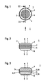
- Fig. 1 shows a piezoelectric component 1 in a schematic representation according to a first embodiment.
- the piezoelectric component 1 can serve in particular as a piezoelectric sensor 1.
- a piezoelectric sensor 1 can be used in particular in fuel injection systems.
- the piezoelectric sensor 1 can serve as a needle-closing sensor, which monitors a closing of a valve needle of a fuel injection valve.
- the sensor 1 can also measure a pressure curve within a fuel space of the fuel injection valve.
- the sensor 1 can also be configured as a combustion chamber pressure sensor 1, which directly or indirectly measures the pressure in a combustion chamber of an internal combustion engine.
- the piezoelectric sensor 1 is also suitable for other applications, especially in the automotive sector.
- the sensor 1 can also be used as an operating medium sensor for hydraulic or pneumatic applications.
- the piezoelectric component 1 serves as a piezoelectric actuator 1.
- the piezoelectric component 1 has a main body 2.
- the main body 2 has an outer side 3, which is designed in this embodiment as a cylinder jacket-shaped outer side 3. Further, an ablation 4 is provided on the base body 2, which is formed by a chamfer 4.
- an outer metallization 5 is provided, which extends in this embodiment over the entire outer side 3 of the main body 2.
- an end-side outer electrode 7 is provided on an end face 6 (FIG. Fig. 2 ) of the main body 2.
- the chamfer 4 separates the outer metallization 5 from the front-side outer electrode 7.
- Fig. 2 shows that in Fig. 1 illustrated piezoelectric component 1 according to the first embodiment in a schematic representation of the in Fig. 1 with II designated viewing direction.
- the main body 2 has a further end face 8, on which a further front-side outer electrode 9 is attached.
- the chamfer 4 is annular and surrounds the end face 6. Furthermore, a further removal 10 is provided, which is formed by a chamfer 10. The chamfer 10 is provided in the region of the further end face 8 and encloses the further end face 8 annularly. By the chamfer 10, the other front-side outer electrode 9 is separated from the outer metallization 5.
- Fig. 3 shows that in Fig. 1 illustrated piezoelectric component 1 according to the first embodiment in a schematic sectional view along in FIG Fig. 1 with III designated cutting line.
- the main body 2 has a first ceramic layer 15, a second ceramic layer 16 and an internal electrode layer 17.
- the inner electrode layer 17 is in this case arranged between the first ceramic layer 15 and the second ceramic layer 16.
- electrical connections can be made in a simple manner to the front-side outer electrode 7, the further outer-side outer electrode 9 and the inner electrode layer 17 External metallization 5 are attached.
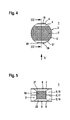
- Fig. 4 shows a piezoelectric component 1 according to a second embodiment in a schematic representation.
- 2 side flats 18, 19 are configured on the base body.
- the outer side 3 of the main body 2 is coated only on the lateral flats 18, 19 with outer metallizations 5, 20. Since the lateral flattenings 18, 19 are configured in a planar manner, the outer metallizations 5, 20 can be easily applied.
- Fig. 5 shows that in Fig. 4 shown piezoelectric component 1 according to the second embodiment in a schematic representation of the in Fig. 4 V direction.
- the chamfer 21 is provided on the one hand on the end face 6 and the front-side outer electrode 7. Further, on the other end 8 or the further front-side outer electrode 9, a further ablation 22 is provided, which is formed by a chamfer 22.
- the chamfers 21, 22 in this case extend in a straight line along the lateral flattening 19, on which the outer metallization 20 is provided.
- FIG. 1 A schematic sectional view of the in Fig. 1 shown piezoelectric device 1 according to the second embodiment along in Fig. 4
- the section line labeled III corresponds to a representation as shown in FIG Fig. 3 is shown.
- Fig. 6 shows a piezoelectric component 1 according to a third embodiment in a schematic representation.
- the base body 2 has exactly one lateral flattening 18, on which the outer metallization 5 is provided.
- the chamfer 4 extends in this case on the end face 6 in a straight line along the lateral flattening 18th
- Fig. 7 shows that in Fig. 6 illustrated piezoelectric component 1 according to the third embodiment in a schematic sectional view along in FIG Fig. 6 with VII designated cutting line.
- the piezoelectric component 1 has exactly one outer metallization 5.
- This outer metallization 5 is configured on one side on the lateral flattening 18 on the outer side 3 of the main body 2.
- a side view from the in Fig. 6 V direction of the piezoelectric component 1 according to the third embodiment is the same as in FIG Fig. 5 shown illustration when in the Fig. 6 V direction is selected.
- Fig. 8 shows a process flow diagram for explaining a method for producing the piezoelectric component 1 according to the first embodiment according to a possible embodiment.
- steps S1 to S5 are shown.
- steps S1, S2 a cross section of a bar-shaped block 30 is shown on the left side in each case. The cross section is in this case selected perpendicular to a longitudinal axis 31 of the rod-shaped block 30.
- steps S1, S2. On the right side, a longitudinal view of the bar-shaped block 30 is shown in steps S1, S2.
- steps S3, S4, S5 a top view of the main body 2 is shown on the left side, as shown in FIG Fig. 1 corresponds to the selected view.
- FIG Fig. 1 corresponds to the selected view.
- Fig. 2 corresponds to the selected view.
- Fig. 3 corresponds to the selected view.
- the rod-shaped block 30 is used as the starting material, which can be prepared as a semi-finished product.
- the rod-shaped block 30 has a multiplicity of ceramic layers 15, 16, 32, 33, 34, 35, 36 and a multiplicity of internal electrode layers 17, 37, 38, 39 arranged between the ceramic layers 15, 16, 32 to 36. 40, 41 on.
- the outer side 3 of the rod-shaped block 30 is designed in the form of a cylinder jacket in this embodiment.
- the rod-shaped block 30 is in this case designed cylindrical.
- step S2 which follows step S1, the outer side 3 is completely provided with an outer metallization 5.
- the outer metallization 5 thus extends along the longitudinal axis 31 over the entire rod-shaped block 30 when the application of the outer metallization 5 is completed.
- the rod-shaped block 30 is separated at parting lines 42 to 48.
- the dividing lines 42 to 48 may in particular be cut lines 42 to 48.
- a diamond saw a separation of the rod-shaped block 30 into individual slices, each with two or more ceramic layers 15, 16, which can be subsequently machined by grinding the front side.
- one of these disks is shown in the form of the main body 2.
- flat end faces 6, 8 are formed, wherein the inner electrode layer 17 is arranged as centrally as possible between the end faces 6, 8. This can be achieved by a suitable choice of the cutting lines 45, 46. Due to the outer metallization 5 applied in step S2 over the entire outer side 3 of the rod-shaped block 30, the outer side 3 of the main body 2 is also initially completely provided with the outer metallization 5. The end faces 6, 8 are still free.
- step S4 which follows step S3, the chamfers 4, 10 on the base body 2 in the region of the end faces 6, 8 are configured.
- step S5 following the step S4, frontal outer electrodes 7, 9 are attached to the end faces 6, 8.
- the outer metallization 5 is now separated on the one hand by the chamfer 4 from the front-side outer electrode 7 and on the other hand by the chamfer 10 of the front-side outer electrode 9.
- step S5 the piezoelectric component 1 is manufactured.
- the rod-shaped block 30 is preferably produced such that the inner electrode layers 17, 37 to 41 are spaced equidistant from each other along the longitudinal axis 31. Accordingly, the dividing lines 42 to 48 are then placed equidistant from each other. Preferably, the dividing lines 43 to 47 are then each in the middle between adjacent inner electrode layers 17, 37 to 41. The outermost dividing lines 42, 48 are then determined in their position due to the predetermined equidistance. As a result, the same size base body 2 are separated, in which the inner electrode layers 17, 37 to 41 each lie between the corresponding end faces 6, 8.
- the metallization of the end faces 6, 8 described with reference to step S5 can be carried out before step S4, in which the chamfers 4, 10 are configured on the base body 2.
- Fig. 9 shows a process flow diagram for explaining a method for producing the piezoelectric component according to the second embodiment according to a possible embodiment.
- method steps S11 to S16 are shown.
- the representation selected in the method steps S11 to S13 corresponds to the representation which is described in the Fig. 8 is selected in the process steps S1, S2.
- the representation selected in the method steps S14 to S16 corresponds to the representation which is described in the Fig. 8 is selected in the process steps S3 to S5.
- the bar-shaped block 30 is manufactured as a semi-finished product.
- layers of the plurality of ceramic layers 15, 16, 32 to 36 and electrode layers 17, 37 to 41 to the block 30 are possible.
- the rod-shaped block 30 is hereby preferably produced as a ceramic multilayer structure. This can be realized by stacking and laminating suitable green sheets, wherein after a certain number of green sheets, in each case an inner electrode paste for the respective inner electrode layer 17, 37 to 41 is applied by printing.
- the rod-shaped blocks 30 thus produced can then be debinded and sintered.
- the production can be partially based on a conventional procedure in which piezoceramic material in the form of rod-shaped semi-finished products is used.
- the rod-shaped block 30 produced in step S11 already has the inner electrode layers 17, 37 to 41 at defined intervals.
- step S12 following step S11 lateral flats 18, 19 are formed on the bar-shaped block 30. This can be done, for example, by grinding the rod-shaped block 30.
- the lateral flats 18, 19 along the longitudinal axis 31 on the entire rod-shaped block 30 are configured.
- step S13 which follows step S12, the associated outer metallization 5, 20 is first applied to the lateral flats 18, 19. The remaining part of the outside 3 remains free here.
- step S13 singulation of the rod-shaped block 30 is performed by a diamond saw or the like.
- the separation takes place along dividing lines 42 to 48.
- this results in the advantage that the inner electrode layers 17, 37 to 41 are optionally visible on the exposed part of the non-metallized outer side 3 and thus can be used to align the cutting tool, in particular the diamond saw.
- step S14 the single base body 2 with the outer metallizations 5, 20 is selected from the plurality of individual discs of the rod-shaped block 30.
- step S15 the edges provided on the end faces 6, 8 between the metallized lateral flats 18, 19 and the end faces 6, 8 are provided with a total of four chamfers 4, 10, 21, 22. Distances between the outer metallizations 5, 20 and the end faces 6, 8 are formed by the chamfers 4, 10, 21, 22.
- step S16 following the step S15 the end faces 6, 8 are provided with front-side outer electrodes 7, 9.
- the chamfers 4, 10, 21, 22 an electrical insulation between the outer metallization 5, the further outer metallization 20, the front-side outer electrode 7 and the front-side outer electrode 9 is ensured.
- the front-side outer electrodes 7, 9 are grounded, while the outer metallizations 5, 20 are used for picking up an electrical signal or for applying an electrical voltage to ground.
- the step S16 in which the front-side outer electrodes 7, 9 are applied, also be carried out before the step S15.
- piezoelectric component 1 Possible applications of the piezoelectric component 1 in possibly correspondingly modified embodiments are multilayer sensors, multilayer actuators or other functional ceramic components 1. In particular, use is also possible in printing and ultrasound applications.
Landscapes
- Engineering & Computer Science (AREA)
- Manufacturing & Machinery (AREA)
- Chemical & Material Sciences (AREA)
- Combustion & Propulsion (AREA)
- Mechanical Engineering (AREA)
- General Engineering & Computer Science (AREA)
- General Electrical Machinery Utilizing Piezoelectricity, Electrostriction Or Magnetostriction (AREA)
- Piezo-Electric Or Mechanical Vibrators, Or Delay Or Filter Circuits (AREA)
Applications Claiming Priority (1)
| Application Number | Priority Date | Filing Date | Title |
|---|---|---|---|
| DE102013200243.2A DE102013200243A1 (de) | 2013-01-10 | 2013-01-10 | Piezoelektrisches Bauteil und Verfahren zur Herstellung eines piezoelektrischen Bauteils |
Publications (3)
| Publication Number | Publication Date |
|---|---|
| EP2755248A2 true EP2755248A2 (fr) | 2014-07-16 |
| EP2755248A3 EP2755248A3 (fr) | 2017-09-13 |
| EP2755248B1 EP2755248B1 (fr) | 2019-04-10 |
Family
ID=49553606
Family Applications (1)
| Application Number | Title | Priority Date | Filing Date |
|---|---|---|---|
| EP13192314.6A Not-in-force EP2755248B1 (fr) | 2013-01-10 | 2013-11-11 | Composant piézoélectrique et procédé de fabrication d'un composant piézoélectrique |
Country Status (3)
| Country | Link |
|---|---|
| US (1) | US9453487B2 (fr) |
| EP (1) | EP2755248B1 (fr) |
| DE (1) | DE102013200243A1 (fr) |
Cited By (1)
| Publication number | Priority date | Publication date | Assignee | Title |
|---|---|---|---|---|
| CN110379916A (zh) * | 2019-07-05 | 2019-10-25 | 中国科学院物理研究所 | 压电陶瓷元件的制备方法 |
Families Citing this family (2)
| Publication number | Priority date | Publication date | Assignee | Title |
|---|---|---|---|---|
| CN107636963B (zh) * | 2015-06-12 | 2020-07-28 | 株式会社村田制作所 | 石英片以及石英振子 |
| KR101965171B1 (ko) * | 2018-08-24 | 2019-08-13 | (주)비티비엘 | 초음파센서의 제조방법 |
Citations (1)
| Publication number | Priority date | Publication date | Assignee | Title |
|---|---|---|---|---|
| DE102010000827A1 (de) | 2010-01-12 | 2011-07-14 | Robert Bosch GmbH, 70469 | Kraftstoffinjektor |
Family Cites Families (13)
| Publication number | Priority date | Publication date | Assignee | Title |
|---|---|---|---|---|
| EP1061591A4 (fr) * | 1998-12-18 | 2007-05-02 | Denso Corp | Corps multicouche piezoelectrique |
| JP2000332313A (ja) * | 1999-05-21 | 2000-11-30 | Matsushita Electric Ind Co Ltd | 薄膜圧電型バイモルフ素子及びその応用 |
| CN1330014C (zh) * | 2000-04-27 | 2007-08-01 | 恩德莱斯和豪瑟尔两合公司 | 用于测量装置的压电陶瓷多层元件及其制造方法 |
| WO2002010264A1 (fr) * | 2000-07-28 | 2002-02-07 | The Penn State Research Foundation | Procede de fabrication de dispositifs electroactifs creux |
| JP2002314156A (ja) * | 2001-04-12 | 2002-10-25 | Denso Corp | 圧電体素子 |
| US6859116B2 (en) * | 2001-07-30 | 2005-02-22 | Kyocera Corporation | Piezoelectric resonator |
| JP2003197992A (ja) * | 2001-12-26 | 2003-07-11 | Murata Mfg Co Ltd | 積層型圧電体及びその製造方法 |
| DE102005046118A1 (de) * | 2005-09-27 | 2007-03-29 | Robert Bosch Gmbh | Piezoaktor mit Schutzwiderstand |
| DE102006018034A1 (de) * | 2006-04-19 | 2007-10-31 | Robert Bosch Gmbh | Piezoaktor und Verfahren zu dessen Herstellung |
| JP5521652B2 (ja) * | 2009-03-18 | 2014-06-18 | 株式会社リコー | 圧電アクチュエータ、液体吐出ヘッド及び画像形成装置 |
| DE102009029521A1 (de) * | 2009-09-17 | 2011-03-24 | Robert Bosch Gmbh | Piezoaktor mit spiralförmiger Außenkontaktierung |
| JP5914355B2 (ja) * | 2010-11-30 | 2016-05-11 | オリンパス株式会社 | 圧電アクチュエータ |
| JP5891935B2 (ja) * | 2011-07-04 | 2016-03-23 | 株式会社大真空 | 水晶振動板および当該水晶振動板を用いた水晶振動子 |
-
2013
- 2013-01-10 DE DE102013200243.2A patent/DE102013200243A1/de not_active Withdrawn
- 2013-11-11 EP EP13192314.6A patent/EP2755248B1/fr not_active Not-in-force
-
2014
- 2014-01-10 US US14/152,044 patent/US9453487B2/en not_active Expired - Fee Related
Patent Citations (1)
| Publication number | Priority date | Publication date | Assignee | Title |
|---|---|---|---|---|
| DE102010000827A1 (de) | 2010-01-12 | 2011-07-14 | Robert Bosch GmbH, 70469 | Kraftstoffinjektor |
Cited By (1)
| Publication number | Priority date | Publication date | Assignee | Title |
|---|---|---|---|---|
| CN110379916A (zh) * | 2019-07-05 | 2019-10-25 | 中国科学院物理研究所 | 压电陶瓷元件的制备方法 |
Also Published As
| Publication number | Publication date |
|---|---|
| US9453487B2 (en) | 2016-09-27 |
| DE102013200243A1 (de) | 2014-07-10 |
| US20140191621A1 (en) | 2014-07-10 |
| EP2755248B1 (fr) | 2019-04-10 |
| EP2755248A3 (fr) | 2017-09-13 |
Similar Documents
| Publication | Publication Date | Title |
|---|---|---|
| EP1908131B1 (fr) | Procede de fabrication d'un actionneur piezoelectrique monolithique a sections d'empilement, actionneur piezoelectrique monolithique a sections d'empilement et utilisation dudit actionneur piezoelectrique | |
| EP1008193B1 (fr) | Procede de production d'actionneurs piezo-electriques, et actionneur piezo-electrique | |
| DE19860001C2 (de) | Piezoelektrisches Bauelement, Verfahren zu dessen Herstellung und Verwendung eines derartigen Bauelements | |
| WO2006103154A1 (fr) | Composant piezo-electrique monolithique comportant une couche de decouplage mecanique, son procede de production et son utilisation | |
| DE102006003070B3 (de) | Verfahren zum elektrischen Kontakieren eines elektronischen Bauelements | |
| EP2755248B1 (fr) | Composant piézoélectrique et procédé de fabrication d'un composant piézoélectrique | |
| EP2543085B9 (fr) | Composant piézoélectrique | |
| DE102008042232A1 (de) | Laminiertes piezoelektrisches Element und Verfahren, dieses herzustellen | |
| EP1233462B1 (fr) | Actionneur multicouche avec zones déplacées de contact des électrodes intérieures ayant la même polarisation que leur électrode extérieur | |
| DE102013206933A1 (de) | Modulare Aktuatoreinheit für ein Einspritzventil | |
| EP2798679B1 (fr) | Pile piézo-électrique avec passivation et procédé de passivation d'une pile piézo-électrique | |
| DE102012221084A1 (de) | Drucksensor und Komponente einer Brennstoffeinspritzanlage mit einem Drucksensor | |
| EP1821351B1 (fr) | Méthode pour produire un dispositif piézoélectrique | |
| DE102017108384A1 (de) | Vielschichtbauelement und Verfahren zur Herstellung eines Vielschichtbauelements | |
| DE102006001656A1 (de) | Piezoaktor und Verfahren zur Herstellung desselben | |
| WO2009156202A1 (fr) | Procédé de fabrication d’un actionneur piézoélectrique empilé et actionneur piézoélectrique | |
| EP3036431B1 (fr) | Actionneur piézo-électrique pour injecteur de carburant et injecteur de carburant | |
| DE102006046217B3 (de) | Verfahren und Vorrichtung zur Herstellung von Keramikstapeln mit vieleckigem Querschnitt | |
| DE102015217334B3 (de) | Verfahren zum Herstellen eines als Stapel ausgebildeten Vielschichtaktors | |
| DD293689A5 (de) | Laminierte keramikanordnung und verfahren zur herstellung derselben | |
| DE102010008775A1 (de) | Piezoelektrisches Vielschichtbauelement und Verfahren zur Herstellung eines piezoelektrischen Vielschichtbauelements | |
| DE102009020238A1 (de) | Piezoaktor mit elektrischen Kontaktierungsstiften | |
| DE102011078915A1 (de) | Sensoranordnung zur Kraft- oder Druckmessung sowie Kraftstoffinjektor mit einer solchen Sensoranordnung | |
| WO2012031942A1 (fr) | Procédé de fabrication d'actionneurs piézoélectriques à partir d'un bloc de matériau | |
| DE102011089773A1 (de) | Piezoelektrischer Aktor und Brennstoffeinspritzventil |
Legal Events
| Date | Code | Title | Description |
|---|---|---|---|
| PUAI | Public reference made under article 153(3) epc to a published international application that has entered the european phase |
Free format text: ORIGINAL CODE: 0009012 |
|
| 17P | Request for examination filed |
Effective date: 20131111 |
|
| AK | Designated contracting states |
Kind code of ref document: A2 Designated state(s): AL AT BE BG CH CY CZ DE DK EE ES FI FR GB GR HR HU IE IS IT LI LT LU LV MC MK MT NL NO PL PT RO RS SE SI SK SM TR |
|
| AX | Request for extension of the european patent |
Extension state: BA ME |
|
| PUAL | Search report despatched |
Free format text: ORIGINAL CODE: 0009013 |
|
| AK | Designated contracting states |
Kind code of ref document: A3 Designated state(s): AL AT BE BG CH CY CZ DE DK EE ES FI FR GB GR HR HU IE IS IT LI LT LU LV MC MK MT NL NO PL PT RO RS SE SI SK SM TR |
|
| AX | Request for extension of the european patent |
Extension state: BA ME |
|
| RIC1 | Information provided on ipc code assigned before grant |
Ipc: H01L 41/29 20130101ALI20170804BHEP Ipc: H01L 41/338 20130101ALI20170804BHEP Ipc: H01L 41/113 20060101ALN20170804BHEP Ipc: H01L 41/293 20130101ALI20170804BHEP Ipc: H01L 41/09 20060101ALN20170804BHEP Ipc: H01L 41/083 20060101AFI20170804BHEP Ipc: H01L 41/047 20060101ALI20170804BHEP Ipc: H01L 41/273 20130101ALI20170804BHEP |
|
| STAA | Information on the status of an ep patent application or granted ep patent |
Free format text: STATUS: REQUEST FOR EXAMINATION WAS MADE |
|
| R17P | Request for examination filed (corrected) |
Effective date: 20180313 |
|
| RBV | Designated contracting states (corrected) |
Designated state(s): AL AT BE BG CH CY CZ DE DK EE ES FI FR GB GR HR HU IE IS IT LI LT LU LV MC MK MT NL NO PL PT RO RS SE SI SK SM TR |
|
| STAA | Information on the status of an ep patent application or granted ep patent |
Free format text: STATUS: EXAMINATION IS IN PROGRESS |
|
| 17Q | First examination report despatched |
Effective date: 20180517 |
|
| RIC1 | Information provided on ipc code assigned before grant |
Ipc: H01L 41/09 20060101ALN20181009BHEP Ipc: H01L 41/29 20130101ALI20181009BHEP Ipc: H01L 41/273 20130101ALI20181009BHEP Ipc: H01L 41/293 20130101ALI20181009BHEP Ipc: H01L 41/337 20130101ALI20181009BHEP Ipc: H01L 41/083 20060101AFI20181009BHEP Ipc: H01L 41/113 20060101ALN20181009BHEP Ipc: H01L 41/047 20060101ALI20181009BHEP Ipc: H01L 41/338 20130101ALI20181009BHEP |
|
| GRAP | Despatch of communication of intention to grant a patent |
Free format text: ORIGINAL CODE: EPIDOSNIGR1 |
|
| STAA | Information on the status of an ep patent application or granted ep patent |
Free format text: STATUS: GRANT OF PATENT IS INTENDED |
|
| INTG | Intention to grant announced |
Effective date: 20181123 |
|
| GRAS | Grant fee paid |
Free format text: ORIGINAL CODE: EPIDOSNIGR3 |
|
| GRAA | (expected) grant |
Free format text: ORIGINAL CODE: 0009210 |
|
| STAA | Information on the status of an ep patent application or granted ep patent |
Free format text: STATUS: THE PATENT HAS BEEN GRANTED |
|
| AK | Designated contracting states |
Kind code of ref document: B1 Designated state(s): AL AT BE BG CH CY CZ DE DK EE ES FI FR GB GR HR HU IE IS IT LI LT LU LV MC MK MT NL NO PL PT RO RS SE SI SK SM TR |
|
| REG | Reference to a national code |
Ref country code: GB Ref legal event code: FG4D Free format text: NOT ENGLISH |
|
| REG | Reference to a national code |
Ref country code: CH Ref legal event code: EP Ref country code: AT Ref legal event code: REF Ref document number: 1119876 Country of ref document: AT Kind code of ref document: T Effective date: 20190415 |
|
| REG | Reference to a national code |
Ref country code: IE Ref legal event code: FG4D Free format text: LANGUAGE OF EP DOCUMENT: GERMAN |
|
| REG | Reference to a national code |
Ref country code: DE Ref legal event code: R096 Ref document number: 502013012581 Country of ref document: DE |
|
| REG | Reference to a national code |
Ref country code: NL Ref legal event code: MP Effective date: 20190410 |
|
| REG | Reference to a national code |
Ref country code: LT Ref legal event code: MG4D |
|
| PG25 | Lapsed in a contracting state [announced via postgrant information from national office to epo] |
Ref country code: NL Free format text: LAPSE BECAUSE OF FAILURE TO SUBMIT A TRANSLATION OF THE DESCRIPTION OR TO PAY THE FEE WITHIN THE PRESCRIBED TIME-LIMIT Effective date: 20190410 |
|
| PG25 | Lapsed in a contracting state [announced via postgrant information from national office to epo] |
Ref country code: LT Free format text: LAPSE BECAUSE OF FAILURE TO SUBMIT A TRANSLATION OF THE DESCRIPTION OR TO PAY THE FEE WITHIN THE PRESCRIBED TIME-LIMIT Effective date: 20190410 Ref country code: HR Free format text: LAPSE BECAUSE OF FAILURE TO SUBMIT A TRANSLATION OF THE DESCRIPTION OR TO PAY THE FEE WITHIN THE PRESCRIBED TIME-LIMIT Effective date: 20190410 Ref country code: NO Free format text: LAPSE BECAUSE OF FAILURE TO SUBMIT A TRANSLATION OF THE DESCRIPTION OR TO PAY THE FEE WITHIN THE PRESCRIBED TIME-LIMIT Effective date: 20190710 Ref country code: FI Free format text: LAPSE BECAUSE OF FAILURE TO SUBMIT A TRANSLATION OF THE DESCRIPTION OR TO PAY THE FEE WITHIN THE PRESCRIBED TIME-LIMIT Effective date: 20190410 Ref country code: PT Free format text: LAPSE BECAUSE OF FAILURE TO SUBMIT A TRANSLATION OF THE DESCRIPTION OR TO PAY THE FEE WITHIN THE PRESCRIBED TIME-LIMIT Effective date: 20190910 Ref country code: SE Free format text: LAPSE BECAUSE OF FAILURE TO SUBMIT A TRANSLATION OF THE DESCRIPTION OR TO PAY THE FEE WITHIN THE PRESCRIBED TIME-LIMIT Effective date: 20190410 Ref country code: AL Free format text: LAPSE BECAUSE OF FAILURE TO SUBMIT A TRANSLATION OF THE DESCRIPTION OR TO PAY THE FEE WITHIN THE PRESCRIBED TIME-LIMIT Effective date: 20190410 Ref country code: ES Free format text: LAPSE BECAUSE OF FAILURE TO SUBMIT A TRANSLATION OF THE DESCRIPTION OR TO PAY THE FEE WITHIN THE PRESCRIBED TIME-LIMIT Effective date: 20190410 |
|
| PG25 | Lapsed in a contracting state [announced via postgrant information from national office to epo] |
Ref country code: BG Free format text: LAPSE BECAUSE OF FAILURE TO SUBMIT A TRANSLATION OF THE DESCRIPTION OR TO PAY THE FEE WITHIN THE PRESCRIBED TIME-LIMIT Effective date: 20190710 Ref country code: RS Free format text: LAPSE BECAUSE OF FAILURE TO SUBMIT A TRANSLATION OF THE DESCRIPTION OR TO PAY THE FEE WITHIN THE PRESCRIBED TIME-LIMIT Effective date: 20190410 Ref country code: LV Free format text: LAPSE BECAUSE OF FAILURE TO SUBMIT A TRANSLATION OF THE DESCRIPTION OR TO PAY THE FEE WITHIN THE PRESCRIBED TIME-LIMIT Effective date: 20190410 Ref country code: PL Free format text: LAPSE BECAUSE OF FAILURE TO SUBMIT A TRANSLATION OF THE DESCRIPTION OR TO PAY THE FEE WITHIN THE PRESCRIBED TIME-LIMIT Effective date: 20190410 Ref country code: GR Free format text: LAPSE BECAUSE OF FAILURE TO SUBMIT A TRANSLATION OF THE DESCRIPTION OR TO PAY THE FEE WITHIN THE PRESCRIBED TIME-LIMIT Effective date: 20190711 |
|
| PG25 | Lapsed in a contracting state [announced via postgrant information from national office to epo] |
Ref country code: IS Free format text: LAPSE BECAUSE OF FAILURE TO SUBMIT A TRANSLATION OF THE DESCRIPTION OR TO PAY THE FEE WITHIN THE PRESCRIBED TIME-LIMIT Effective date: 20190810 |
|
| REG | Reference to a national code |
Ref country code: DE Ref legal event code: R097 Ref document number: 502013012581 Country of ref document: DE |
|
| PG25 | Lapsed in a contracting state [announced via postgrant information from national office to epo] |
Ref country code: EE Free format text: LAPSE BECAUSE OF FAILURE TO SUBMIT A TRANSLATION OF THE DESCRIPTION OR TO PAY THE FEE WITHIN THE PRESCRIBED TIME-LIMIT Effective date: 20190410 Ref country code: DK Free format text: LAPSE BECAUSE OF FAILURE TO SUBMIT A TRANSLATION OF THE DESCRIPTION OR TO PAY THE FEE WITHIN THE PRESCRIBED TIME-LIMIT Effective date: 20190410 Ref country code: CZ Free format text: LAPSE BECAUSE OF FAILURE TO SUBMIT A TRANSLATION OF THE DESCRIPTION OR TO PAY THE FEE WITHIN THE PRESCRIBED TIME-LIMIT Effective date: 20190410 Ref country code: RO Free format text: LAPSE BECAUSE OF FAILURE TO SUBMIT A TRANSLATION OF THE DESCRIPTION OR TO PAY THE FEE WITHIN THE PRESCRIBED TIME-LIMIT Effective date: 20190410 Ref country code: SK Free format text: LAPSE BECAUSE OF FAILURE TO SUBMIT A TRANSLATION OF THE DESCRIPTION OR TO PAY THE FEE WITHIN THE PRESCRIBED TIME-LIMIT Effective date: 20190410 |
|
| PLBE | No opposition filed within time limit |
Free format text: ORIGINAL CODE: 0009261 |
|
| STAA | Information on the status of an ep patent application or granted ep patent |
Free format text: STATUS: NO OPPOSITION FILED WITHIN TIME LIMIT |
|
| PG25 | Lapsed in a contracting state [announced via postgrant information from national office to epo] |
Ref country code: SM Free format text: LAPSE BECAUSE OF FAILURE TO SUBMIT A TRANSLATION OF THE DESCRIPTION OR TO PAY THE FEE WITHIN THE PRESCRIBED TIME-LIMIT Effective date: 20190410 Ref country code: IT Free format text: LAPSE BECAUSE OF FAILURE TO SUBMIT A TRANSLATION OF THE DESCRIPTION OR TO PAY THE FEE WITHIN THE PRESCRIBED TIME-LIMIT Effective date: 20190410 |
|
| PGFP | Annual fee paid to national office [announced via postgrant information from national office to epo] |
Ref country code: FR Payment date: 20191121 Year of fee payment: 7 |
|
| 26N | No opposition filed |
Effective date: 20200113 |
|
| PG25 | Lapsed in a contracting state [announced via postgrant information from national office to epo] |
Ref country code: TR Free format text: LAPSE BECAUSE OF FAILURE TO SUBMIT A TRANSLATION OF THE DESCRIPTION OR TO PAY THE FEE WITHIN THE PRESCRIBED TIME-LIMIT Effective date: 20190410 |
|
| PGFP | Annual fee paid to national office [announced via postgrant information from national office to epo] |
Ref country code: DE Payment date: 20200124 Year of fee payment: 7 |
|
| PG25 | Lapsed in a contracting state [announced via postgrant information from national office to epo] |
Ref country code: SI Free format text: LAPSE BECAUSE OF FAILURE TO SUBMIT A TRANSLATION OF THE DESCRIPTION OR TO PAY THE FEE WITHIN THE PRESCRIBED TIME-LIMIT Effective date: 20190410 |
|
| REG | Reference to a national code |
Ref country code: CH Ref legal event code: PL |
|
| PG25 | Lapsed in a contracting state [announced via postgrant information from national office to epo] |
Ref country code: CH Free format text: LAPSE BECAUSE OF NON-PAYMENT OF DUE FEES Effective date: 20191130 Ref country code: LU Free format text: LAPSE BECAUSE OF NON-PAYMENT OF DUE FEES Effective date: 20191111 Ref country code: MC Free format text: LAPSE BECAUSE OF FAILURE TO SUBMIT A TRANSLATION OF THE DESCRIPTION OR TO PAY THE FEE WITHIN THE PRESCRIBED TIME-LIMIT Effective date: 20190410 Ref country code: LI Free format text: LAPSE BECAUSE OF NON-PAYMENT OF DUE FEES Effective date: 20191130 |
|
| REG | Reference to a national code |
Ref country code: BE Ref legal event code: MM Effective date: 20191130 |
|
| GBPC | Gb: european patent ceased through non-payment of renewal fee |
Effective date: 20191111 |
|
| PG25 | Lapsed in a contracting state [announced via postgrant information from national office to epo] |
Ref country code: IE Free format text: LAPSE BECAUSE OF NON-PAYMENT OF DUE FEES Effective date: 20191111 Ref country code: GB Free format text: LAPSE BECAUSE OF NON-PAYMENT OF DUE FEES Effective date: 20191111 |
|
| PG25 | Lapsed in a contracting state [announced via postgrant information from national office to epo] |
Ref country code: BE Free format text: LAPSE BECAUSE OF NON-PAYMENT OF DUE FEES Effective date: 20191130 |
|
| REG | Reference to a national code |
Ref country code: AT Ref legal event code: MM01 Ref document number: 1119876 Country of ref document: AT Kind code of ref document: T Effective date: 20191111 |
|
| PG25 | Lapsed in a contracting state [announced via postgrant information from national office to epo] |
Ref country code: AT Free format text: LAPSE BECAUSE OF NON-PAYMENT OF DUE FEES Effective date: 20191111 |
|
| PG25 | Lapsed in a contracting state [announced via postgrant information from national office to epo] |
Ref country code: CY Free format text: LAPSE BECAUSE OF FAILURE TO SUBMIT A TRANSLATION OF THE DESCRIPTION OR TO PAY THE FEE WITHIN THE PRESCRIBED TIME-LIMIT Effective date: 20190410 |
|
| REG | Reference to a national code |
Ref country code: DE Ref legal event code: R119 Ref document number: 502013012581 Country of ref document: DE |
|
| PG25 | Lapsed in a contracting state [announced via postgrant information from national office to epo] |
Ref country code: HU Free format text: LAPSE BECAUSE OF FAILURE TO SUBMIT A TRANSLATION OF THE DESCRIPTION OR TO PAY THE FEE WITHIN THE PRESCRIBED TIME-LIMIT; INVALID AB INITIO Effective date: 20131111 Ref country code: MT Free format text: LAPSE BECAUSE OF FAILURE TO SUBMIT A TRANSLATION OF THE DESCRIPTION OR TO PAY THE FEE WITHIN THE PRESCRIBED TIME-LIMIT Effective date: 20190410 |
|
| PG25 | Lapsed in a contracting state [announced via postgrant information from national office to epo] |
Ref country code: FR Free format text: LAPSE BECAUSE OF NON-PAYMENT OF DUE FEES Effective date: 20201130 |
|
| PG25 | Lapsed in a contracting state [announced via postgrant information from national office to epo] |
Ref country code: DE Free format text: LAPSE BECAUSE OF NON-PAYMENT OF DUE FEES Effective date: 20210601 |
|
| PG25 | Lapsed in a contracting state [announced via postgrant information from national office to epo] |
Ref country code: MK Free format text: LAPSE BECAUSE OF FAILURE TO SUBMIT A TRANSLATION OF THE DESCRIPTION OR TO PAY THE FEE WITHIN THE PRESCRIBED TIME-LIMIT Effective date: 20190410 |