EP2757414A2 - Système optique de source lumineuse pour un projecteur - Google Patents
Système optique de source lumineuse pour un projecteur Download PDFInfo
- Publication number
- EP2757414A2 EP2757414A2 EP13181330.5A EP13181330A EP2757414A2 EP 2757414 A2 EP2757414 A2 EP 2757414A2 EP 13181330 A EP13181330 A EP 13181330A EP 2757414 A2 EP2757414 A2 EP 2757414A2
- Authority
- EP
- European Patent Office
- Prior art keywords
- light
- phosphor element
- optical system
- module
- solid
- Prior art date
- Legal status (The legal status is an assumption and is not a legal conclusion. Google has not performed a legal analysis and makes no representation as to the accuracy of the status listed.)
- Granted
Links
Images


Classifications
-
- G—PHYSICS
- G03—PHOTOGRAPHY; CINEMATOGRAPHY; ANALOGOUS TECHNIQUES USING WAVES OTHER THAN OPTICAL WAVES; ELECTROGRAPHY; HOLOGRAPHY
- G03B—APPARATUS OR ARRANGEMENTS FOR TAKING PHOTOGRAPHS OR FOR PROJECTING OR VIEWING THEM; APPARATUS OR ARRANGEMENTS EMPLOYING ANALOGOUS TECHNIQUES USING WAVES OTHER THAN OPTICAL WAVES; ACCESSORIES THEREFOR
- G03B21/00—Projectors or projection-type viewers; Accessories therefor
- G03B21/14—Details
- G03B21/20—Lamp housings
- G03B21/2006—Lamp housings characterised by the light source
- G03B21/2033—LED or laser light sources
- G03B21/204—LED or laser light sources using secondary light emission, e.g. luminescence or fluorescence
-
- G—PHYSICS
- G03—PHOTOGRAPHY; CINEMATOGRAPHY; ANALOGOUS TECHNIQUES USING WAVES OTHER THAN OPTICAL WAVES; ELECTROGRAPHY; HOLOGRAPHY
- G03B—APPARATUS OR ARRANGEMENTS FOR TAKING PHOTOGRAPHS OR FOR PROJECTING OR VIEWING THEM; APPARATUS OR ARRANGEMENTS EMPLOYING ANALOGOUS TECHNIQUES USING WAVES OTHER THAN OPTICAL WAVES; ACCESSORIES THEREFOR
- G03B21/00—Projectors or projection-type viewers; Accessories therefor
- G03B21/005—Projectors using an electronic spatial light modulator but not peculiar thereto
-
- G—PHYSICS
- G03—PHOTOGRAPHY; CINEMATOGRAPHY; ANALOGOUS TECHNIQUES USING WAVES OTHER THAN OPTICAL WAVES; ELECTROGRAPHY; HOLOGRAPHY
- G03B—APPARATUS OR ARRANGEMENTS FOR TAKING PHOTOGRAPHS OR FOR PROJECTING OR VIEWING THEM; APPARATUS OR ARRANGEMENTS EMPLOYING ANALOGOUS TECHNIQUES USING WAVES OTHER THAN OPTICAL WAVES; ACCESSORIES THEREFOR
- G03B21/00—Projectors or projection-type viewers; Accessories therefor
- G03B21/14—Details
- G03B21/20—Lamp housings
- G03B21/208—Homogenising, shaping of the illumination light
-
- H—ELECTRICITY
- H04—ELECTRIC COMMUNICATION TECHNIQUE
- H04N—PICTORIAL COMMUNICATION, e.g. TELEVISION
- H04N9/00—Details of colour television systems
- H04N9/12—Picture reproducers
- H04N9/31—Projection devices for colour picture display, e.g. using electronic spatial light modulators [ESLM]
- H04N9/3141—Constructional details thereof
- H04N9/315—Modulator illumination systems
- H04N9/3161—Modulator illumination systems using laser light sources
Definitions
- the present invention provides an optical system, and more particularly, to an optical system for a projector.
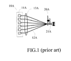
- FIG. 1 shows that in such an optical system, a solid-state light source module 10A has a plurality of laser diodes 11A. Each of the laser diodes 11A is adapted to generate a laser beam 12A respectively. The laser beams 12A are then converged by a lens 13A onto a phosphor element 20A so that the phosphor element 20A is excited to emit light beams 21A of a specific color (i.e. wavelength).
- this kind of optical system has at least the following two shortcomings.
- the laser beams 12A that are converged by the lens 13A and the converged laser beams 12A are incident onto the phosphor element 20A, and the light intensity on phosphor element 20A could be not uniform because the laser beams 12A could be not well aligned in practical manufacture.
- some regions of the phosphor element 20A are irradiated by more of the laser beams 12A, while some other regions are irradiated by less of the laser beams 12A.
- the higher temperature may decrease the exciting efficiency of the phosphor element 20A. That is, the exciting efficiency of the phosphor on the phosphor element may degrade as the temperature increases and cannot achieve the optimal exciting efficiency.
- a light spot of the laser beams 12A incident on the phosphor element 20A is not appropriately designed in terms of the shape and area thereof. This often leads to an overlarge emission area of the phosphor element 20A. That is, the Etendue of emission light of the phosphor element 20A becomes larger than what is acceptable for the light modulator (not shown) of the projector. As a consequence, light is lost because a part of the excited light beams 21A cannot be utilized by the light modulator. It shall be appreciated that the Etendue is defined as the product of a light source area and the divergence solid angle and is used to represent the geometric properties of an optical system.
- the positions of the individual laser diodes 11A as well as the angles and directions of the laser beams 12A must be precisely tailored and, further, all optical components between the laser diodes 11A and the phosphor element 20A must be precisely aligned.
- the laser beams 12A can be uniformly incident on the phosphor element 20A and form a light spot of an appropriated shape and an appropriate area on the phosphor element 20A.
- this consumes time and costs and is difficult to control in practice, which is unfavorable for the production of the projector. Therefore, cheap projectors will have phosphor elements with poor exciting efficiencies and big production tolerance, and will not be able to make optimal exciting efficiency of phosphor and efficient use of the excited light beams.
- An objective of the present invention is to provide an optical system in which a phosphor element can easily have a good exciting efficiency.
- Another objective of the present invention is to provide another optical system by which a projector can efficiently utilize the light excited from the phosphor element.
- an optical system disclosed in the present invention can be used in a projector.
- the optical system comprises the following components: a solid-state light source module for generating a first light beams; an optical module that is disposed on the side of the solid-state light source module; a phosphor element that is disposed on the side of the optical module, wherein the optical module is disposed between the solid-state light source module and the phosphor element in a light path; and a light relay module that is disposed on the side of the phosphor element, wherein the phosphor element is disposed between the optical module and the light relay module in the light path; wherein, the optical module is used for relaying and uniformizing the first light beams so that the first light beams is uniformly incident on the phosphor element.
- the optical module is also used for making the light spot of the first light beams incident on the phosphor element with a predetermined shape and predetermined area so that the phosphor element emits the second light beams in the emitting area; wherein, the light relay module is used for receiving a part of the second light beams.
- the part of the second light beams has a solid angle; wherein, an Etendue defined by the solid angle and the emitting area is substantially identical to the acceptable Etendue of a light modulator of the projector.
- FIGs. 2 and 3 show two schematic plan views of an optical system according to the first embodiment of the present invention respectively.
- an optical system 1 is proposed.
- the optical system 1 can be used in a projector and may be considered as a part of the projector.
- the optical system 1 comprises a solid-state light source module 10, an optical module 20, a phosphor element 30, and a light relay module 35.
- a light modulator 40, a projection lens 50, a light uniformizing element 53 or a light relaying module 55 and other components of the projector that are to be described later may also be considered to be comprised in the optical system 1.
- the solid-state light source module 10, the optical module 20, the phosphor element 30 and the light relay module 35 are disposed sequentially. That is, the optical module 20 is disposed at a side (e.g., the back side) of the solid-state light source module 10, the phosphor element 30 is disposed at a side (e.g., the back side) of the optical module 20, and the light relay module 35 is disposed at a side (e.g., the back side) of the phosphor element 30.
- the optical module 20 is disposed between the solid-state light source module 10 and the phosphor element 30 in a light path, while the phosphor element 30 is disposed between the optical module 20 and the light relay module 35 in the light path.
- solid-state light source module 10 the optical module 20, the phosphor element 30, the light relay module 35 and the light modulator 40 and the like are sequentially described as follows.
- FIG. 4 is a schematic plan view of the solid-state light source module of the optical system of FIG. 2 .
- the solid-state light source module 10 may have a plurality of solid-state light sources 11. Each of the solid-state light sources 11 may be a laser diode or a light-emitting diode, and in this embodiment, is illustrated as a laser diode.
- the solid-state light source module 10 may further optionally comprise a plurality of collimator lenses 12.
- the collimator lenses 12 are disposed at a side of the solid-state light sources 11 respectively to receive light beams 111 emitted from the solid-state light sources 11 so that the light beams 111 can be more collimated.
- the solid-state light sources 11 are further disposed in such a way that the emitted light beams 111 have a good parallelism.
- the light beams 111 generated by the solid-state light sources 11 can be collectively viewed as a first beam 13.
- the solid-state light source module 10 as a whole can generate a first beam 13 by the solid-state light sources 11. Since all the light beams 111 are well collimated, the first beam 13 as a whole is also well collimated.
- the optical module 20 can relay and uniformize the first beam 13, and may have an integration rod 21 and at least one relay lens 22.
- the optical module 20 can relay and uniformize the first beam 13, and may have an integration rod 21 and at least one relay lens 22.
- three relay lenses 22 are shown for illustration.
- the first beam 13 can be converged and relayed to the integration rod 21 by a first relay lens 22 to be uniformized by the integration rod 21. That is, when passing through the integration rod 21, the first beam 13 is reflected or total internal reflected in the integration rod 21 so that the light intensity of the first beam 13 exiting from the integration rod 21 is relatively uniform.
- the integration rod 21 may be of a solid or hollow structure.
- the phosphor element 30 may be a fixed phosphor plate or a rotary phosphor wheel, and may either be a transmissive phosphor element or a reflective phosphor element.
- FIG. 5 is a schematic diagram illustrating the temperature versus the emitting efficiency of the phosphor element of the optical system of FIG. 2 .
- the maximum emitting efficiency of the phosphor element 30 corresponds to a specific temperature which is, for example, about 40 degrees (which is only for illustration).
- the exciting efficiency degradation cannot only caused by temperature, the higher laser pumping power intensity, the lower exciting efficiency. So the more uniform laser light incident on the phosphor the lower laser power intensity, which is also helpful on getting better exciting efficiency of phosphor.
- FIG. 6 is a schematic view illustrating a light spot of the first beam and the phosphor element of the optical system of FIG. 2 .
- the optical module 20 can further make the light spot 131 of the first beam 13 incident on the phosphor element 30 have a predetermined area (i.e., a predetermined size) and a predetermined shape.
- the predetermined shape of the light spot 131 is designed to be identical to (or similar to) the shape of the light modulator 40 (as shown in FIG. 7 ). Therefore, if the light modulator 40 is in a rectangular shape, then the predetermined shape of the light spot 131 is identical to or similar to the rectangular shape.
- the predetermined shape of the light spot 131 is associated with the shape of an output aperture 211 of the integration rod 21.
- the first beam 13 passing through the integration rod 21 is not only uniformized but also shaped by the integration rod 21 to make the sectional shape of the first beam 13 along the main optical axis identical to or similar to the shape of the output aperture 211 of the integration rod 21.
- the predetermined shape of the light spot 131 after being shaped is identical to the shape of the output aperture 211 of the integration rod 21.
- the predetermined shape of the light spot 131 after being shaped is not identical to the shape of the output aperture 211 of the integration rod 21, but is identical to the shape of "the output aperture 211 of the integration rod 21 that is projected onto the phosphor element 30 along the main optical axis of the first beam 13".
- the predetermined shape of the light spot 131 is required to be a rectangular shape (the aspect ratio of which is 4:3), then, when the phosphor element 30 is perpendicular to the main optical axis of the first beam 13, the output aperture 211 of the integration rod 21 may be designed into the same rectangular shape. However, if the phosphor element 30 is inclined to the main optical axis of the first beam 13, the output aperture 211 of the integration rod 21 is designed into a different rectangular shape (the aspect ratio of which is not 4:3).
- the predetermined area of the light spot 131 is associated with the "area of the output aperture 211 of the integration rod 21" and "the magnification of the relay optics from rod to phosphor element (herein the relay optics is lens 22)."
- the area of the light spot 131 is defined as "the product of the area of the output aperture 211 and the magnification of the relay lens 22". Therefore, the predetermined area of the light spot 131 can be obtained by adjusting the area of the output aperture 211 and/or the magnification of the relay lens 22.
- the angle included between the phosphor element 30 and the main optical axis of the first beam 13 shall be considered in determination of the predetermined area of the light spot 131 to obtain the desired area of the light spot 131.
- the phosphor element 30 can emit a second beam 31 in an emitting area A2.
- the light relay module 35 may comprise at least one lens 351, and in this embodiment, two lenses 351 are shown for illustration.
- the light relay module 35 can receive a part 311 of the second beam 31. That is, not all the second beam 31 is received by the light relay module 35, and the light rays outside of the receiving range of the light relay module 35 will not enter the light relay module 35.
- the part 311 of the second beam 31 has a solid angle ⁇ 1 .
- the solid angle ⁇ 1 corresponds to the light receiving ability of the light relay module 35; that is, the greater the part 311 of the second beam 31 that can be received by the light relay module 35, the larger the solid angle ⁇ 1 of the part 311 of the second beam 31.
- the Etendue E p defined by the solid angle ⁇ 1 and the emitting area A2 is substantially equal to a usable Etendue E m of the light modulator 40 of the projector.
- FIG. 7 is a schematic plan view of the light modulator and the projection lens according to the first embodiment of the present invention.
- the light modulator 40 may be a digital micromirror device (DMD), a liquid crystal on silicon device (LCoS) or a liquid crystal device (LCD).
- the light modulator 40 has a modulator area A1 and a numeral aperture (NA).
- the numeral aperture NA is associated with a usable-light (i.e., receivable light) solid angle ⁇ 2 of the light modulator 40 , and is further associated with an F-number of a projection lens 50 of the projector.
- the Etendue E m of the light modulator 40 is a function of the modulator area A1 and the usable-light solid angle ⁇ 2 .
- the Etendue E p defined by "the solid angle ⁇ 1 of the part 311 of the second beam 31" and "the emitting area A2 of the phosphor element 30" can be determined so that the desired values of the solid angle ⁇ 1 and the emitting area A2 are determined.
- the user may first select the desired value of one of the solid angle ⁇ 1 and the emitting area A2, and then derive the desired value of the other.
- the desired emitting area A2 of the phosphor element 30 can be determined.
- the predetermined area of the light spot 131 can be determined once the desired emitting area A2 is known. Then, the area of the output aperture 211 of the integration rod 21 and/or the magnification of the relay lens 22 are determined.
- the predetermined area of the light spot 131 may be equal to the desired emitting area A2 of the phosphor element 30.
- the predetermined area of the light spot 131 may also be 20mm 2 .
- the predetermined area of the light spot 131 is slightly smaller than the desired emitting area A2 of the phosphor element 30 in consideration of the following factors: the emitting area A2 is in general slightly larger than the irradiation area (i.e., the predetermined area of the light spot 131) due to the thickness of the phosphor element 30, so having the emitting area A2 equal to the predetermined area of the light spot 131 requires that the emitting area A2 exceeds the desired value and, thus, the predetermined area of the light spot 131 needs to be slightly reduced.
- the predetermined area of the light spot 131 is defined by the Etendue E m of the light modulator 40 and the emitting area A2 of the phosphor element 30, and is achieved by adjusting the parameters (e.g., the area of the output aperture 211 of the integration rod 21 and/or the magnification of the relay lens 22) of the optical module 20.
- FIG. 8 is a schematic plan view of the optical system according to the second embodiment of the present invention.
- another optical system 2 is proposed.
- the optical system 2 is different from the optical system 1 in that the optical system 2 comprises an optical module 60 implemented in a different form.
- the optical module 60 has two lens arrays or fly eye arrays 61 and at least one relay lens 62.
- the two lens arrays 61 may be disposed at a side (e.g., the front side) of the relay lens 62, and each of the two lens arrays 61 has a plurality of lenses 611.
- one relay lens 62 is shown for illustration.
- the first beam 13 generated by the solid-state light source module 10 can be directly relayed to the two lens arrays 61 and relay lens 62. Then the light 31 can be converged onto phosphor element 30 as a uniformized and shaped light spot 131, the shape is same with the lens 611, the spot size is determined by the magnification of the optics composed by the two lens arrays 61 and relay lens 62. As a result, a second beam 31 is emitted by the phosphor element 30 in an emitting area A2.
- FIG. 3 illustrates the part 311 of the second beam 31 that can then be received by the light relay module 35.
- the Etendue E p defined by the solid angle ⁇ 1 of the part 311 of the second beam 31 and the emitting area A2 is substantially equal to the Etendue E m of the light modulator 40.
- the light modulator 40 can also make sufficient use of the part 311 of the second beam 31 received by the light relay module 35 in the optical system 2.
- the predetermined shape of the light spot 131 is associated with the shape of the lenses 611 of the lens arrays 61. That is, the predetermined shape of the light spot 131 may be identical to the shape of the lenses 611 or "the shape of the lenses 611 projected onto the phosphor element 30 along the main optical axis of the first beam 13".
- the predetermined area of the light spot 131 is defined by the Etendues of the light modulator (not shown) and the phosphor element 30, and can be achieved by adjusting parameters (e.g., the area of the lenses 611 and/or the magnification of the relay lens 62) of the optical module 60.
- the first beam 13 generated by the solid-state light source module 10 cannot be completely collimated, but still have some diffusion angle.
- the permissible value of the diffusion angle of the first beam 13 is associated with the parameters of the two lens arrays 61.
- the lenses 611 of the two lens arrays 61 have a dimension (a) and a dimension (b) in a first direction and a second direction respectively. There is a distance (d) between the two lens arrays 61 in a third direction.
- the first, the second and the third directions are orthogonal to each other, while the third direction is parallel to the main optical axis of the first beam 13.
- the diffusion angle of the first beam 13 in the first direction should not exceed sin -1 (a/d), and the diffusion angle in the second direction should not exceed sin -1 (b/d). It should be appreciated that the focal length of each of the lenses 611 of the two lens arrays 61 is approximately equal to the distance (d) between the two lens arrays 61.
- the optical system disclosed in the present invention can make the first beam be uniformly incident on the phosphor element to form the light spot of the predetermined shape and area by simply using the optical module instead of using the time-consuming and cost-consuming conventional practice that has to precisely tailor the relative position of the solid-state light source. Therefore, with the optical system disclosed in the present invention, the phosphor element can easily have a good exciting efficiency. The projector can make good use of the light beams excited by the phosphor element.
Landscapes
- Physics & Mathematics (AREA)
- General Physics & Mathematics (AREA)
- Engineering & Computer Science (AREA)
- Multimedia (AREA)
- Optics & Photonics (AREA)
- Signal Processing (AREA)
- Projection Apparatus (AREA)
- Non-Portable Lighting Devices Or Systems Thereof (AREA)
Priority Applications (1)
| Application Number | Priority Date | Filing Date | Title |
|---|---|---|---|
| EP19213129.0A EP3663850B1 (fr) | 2013-01-17 | 2013-08-22 | Système optique de source lumineuse pour un projecteur |
Applications Claiming Priority (1)
| Application Number | Priority Date | Filing Date | Title |
|---|---|---|---|
| TW102101731A TWI459122B (zh) | 2013-01-17 | 2013-01-17 | 光學系統 |
Related Child Applications (2)
| Application Number | Title | Priority Date | Filing Date |
|---|---|---|---|
| EP19213129.0A Division EP3663850B1 (fr) | 2013-01-17 | 2013-08-22 | Système optique de source lumineuse pour un projecteur |
| EP19213129.0A Division-Into EP3663850B1 (fr) | 2013-01-17 | 2013-08-22 | Système optique de source lumineuse pour un projecteur |
Publications (3)
| Publication Number | Publication Date |
|---|---|
| EP2757414A2 true EP2757414A2 (fr) | 2014-07-23 |
| EP2757414A3 EP2757414A3 (fr) | 2016-08-10 |
| EP2757414B1 EP2757414B1 (fr) | 2020-01-08 |
Family
ID=49028949
Family Applications (2)
| Application Number | Title | Priority Date | Filing Date |
|---|---|---|---|
| EP19213129.0A Active EP3663850B1 (fr) | 2013-01-17 | 2013-08-22 | Système optique de source lumineuse pour un projecteur |
| EP13181330.5A Active EP2757414B1 (fr) | 2013-01-17 | 2013-08-22 | Système optique de source lumineuse pour un projecteur |
Family Applications Before (1)
| Application Number | Title | Priority Date | Filing Date |
|---|---|---|---|
| EP19213129.0A Active EP3663850B1 (fr) | 2013-01-17 | 2013-08-22 | Système optique de source lumineuse pour un projecteur |
Country Status (4)
| Country | Link |
|---|---|
| US (1) | US9176368B2 (fr) |
| EP (2) | EP3663850B1 (fr) |
| JP (1) | JP5805719B2 (fr) |
| TW (1) | TWI459122B (fr) |
Cited By (1)
| Publication number | Priority date | Publication date | Assignee | Title |
|---|---|---|---|---|
| EP3173849A1 (fr) * | 2015-11-28 | 2017-05-31 | Canon Kabushiki Kaisha | Système optique de source de lumière et afficheurparprojection l'utilisant |
Families Citing this family (7)
| Publication number | Priority date | Publication date | Assignee | Title |
|---|---|---|---|---|
| JP6327035B2 (ja) * | 2013-08-12 | 2018-05-23 | 大日本印刷株式会社 | 照明装置、投射装置、レンズアレイおよび光学モジュール |
| CN106764470A (zh) * | 2015-11-19 | 2017-05-31 | 深圳市绎立锐光科技开发有限公司 | 一种光源系统及照明装置 |
| JP6828460B2 (ja) * | 2017-01-26 | 2021-02-10 | セイコーエプソン株式会社 | 照明装置及びプロジェクター |
| CN113126404B (zh) * | 2019-12-31 | 2023-08-18 | 深圳光峰科技股份有限公司 | 光源装置 |
| CN111856852B (zh) * | 2020-08-12 | 2021-03-30 | 广东烨嘉光电科技股份有限公司 | 一种微透镜阵列的光学投影系统 |
| CN114815476A (zh) * | 2021-01-19 | 2022-07-29 | 深圳光峰科技股份有限公司 | 一种光源系统以及投影系统 |
| CN113641063B (zh) * | 2021-08-16 | 2023-12-08 | 深圳市火乐科技发展有限公司 | 匀光装置、投影仪光机以及投影仪 |
Family Cites Families (21)
| Publication number | Priority date | Publication date | Assignee | Title |
|---|---|---|---|---|
| JPH0422913A (ja) | 1990-05-18 | 1992-01-27 | Nikon Corp | 色消ビーム整形光学系 |
| JP3589222B2 (ja) | 1999-01-14 | 2004-11-17 | セイコーエプソン株式会社 | 照明光学系および投写型表示装置 |
| JP4055610B2 (ja) * | 2002-03-22 | 2008-03-05 | セイコーエプソン株式会社 | 画像表示デバイス及びプロジェクタ |
| JP4347546B2 (ja) | 2002-06-28 | 2009-10-21 | 株式会社 液晶先端技術開発センター | 結晶化装置、結晶化方法および光学系 |
| KR100611972B1 (ko) | 2003-06-10 | 2006-08-11 | 삼성전자주식회사 | 소형광원모듈 및 이를 채용한 투사형 화상표시장치 |
| JP4411923B2 (ja) | 2003-10-06 | 2010-02-10 | セイコーエプソン株式会社 | 照明装置、表示装置及びプロジェクタ |
| JP4843344B2 (ja) | 2005-03-18 | 2011-12-21 | 株式会社リコー | 照明装置及び画像読取装置 |
| TWI265366B (en) | 2005-06-30 | 2006-11-01 | Chunghwa Picture Tubes Ltd | Light source module and optical projection system |
| CN100432748C (zh) | 2005-07-05 | 2008-11-12 | 中华映管股份有限公司 | 光源模块与光学投影系统 |
| US20070273798A1 (en) | 2006-05-26 | 2007-11-29 | Silverstein Barry D | High efficiency digital cinema projection system with increased etendue |
| WO2008073105A1 (fr) | 2006-12-15 | 2008-06-19 | Thomson Licensing | Module et procédé d'éclairage |
| US7330314B1 (en) | 2007-02-28 | 2008-02-12 | Corning Incorporated | Color combiner for solid-state light sources |
| FR2913750A1 (fr) | 2007-03-14 | 2008-09-19 | Valeo Vision Sa | Module optique pour projecteur de vehicule automobile |
| CN101493207B (zh) | 2008-01-23 | 2011-11-23 | 曹嘉灿 | 固态光源装置、采用该装置的投影系统及集束照明灯具 |
| JP5492582B2 (ja) | 2010-01-29 | 2014-05-14 | 日立コンシューマエレクトロニクス株式会社 | 投写型映像表示装置 |
| US9022580B2 (en) * | 2010-01-29 | 2015-05-05 | Nec Display Solutions, Ltd. | Illumination optical system and projector using the same |
| JP5527594B2 (ja) | 2010-03-24 | 2014-06-18 | カシオ計算機株式会社 | 光源ユニット及びプロジェクタ |
| JP5497912B2 (ja) * | 2010-11-17 | 2014-05-21 | Necディスプレイソリューションズ株式会社 | 光源装置、照明装置および投射型表示装置 |
| JP5699568B2 (ja) | 2010-11-29 | 2015-04-15 | セイコーエプソン株式会社 | 光源装置、プロジェクター |
| JP2012141411A (ja) | 2010-12-28 | 2012-07-26 | Jvc Kenwood Corp | 光源装置 |
| JP5780153B2 (ja) * | 2011-01-24 | 2015-09-16 | 株式会社Jvcケンウッド | 光源装置及び投射型表示装置 |
-
2013
- 2013-01-17 TW TW102101731A patent/TWI459122B/zh active
- 2013-08-06 US US13/959,812 patent/US9176368B2/en active Active
- 2013-08-22 EP EP19213129.0A patent/EP3663850B1/fr active Active
- 2013-08-22 EP EP13181330.5A patent/EP2757414B1/fr active Active
- 2013-08-28 JP JP2013176805A patent/JP5805719B2/ja active Active
Non-Patent Citations (1)
| Title |
|---|
| None |
Cited By (2)
| Publication number | Priority date | Publication date | Assignee | Title |
|---|---|---|---|---|
| EP3173849A1 (fr) * | 2015-11-28 | 2017-05-31 | Canon Kabushiki Kaisha | Système optique de source de lumière et afficheurparprojection l'utilisant |
| US9921462B2 (en) | 2015-11-28 | 2018-03-20 | Canon Kabushiki Kaisha | Light source optical system and projection display apparatus employing the same |
Also Published As
| Publication number | Publication date |
|---|---|
| TW201430474A (zh) | 2014-08-01 |
| JP2014137593A (ja) | 2014-07-28 |
| EP3663850A1 (fr) | 2020-06-10 |
| EP3663850B1 (fr) | 2021-05-05 |
| US20140198303A1 (en) | 2014-07-17 |
| JP5805719B2 (ja) | 2015-11-04 |
| TWI459122B (zh) | 2014-11-01 |
| EP2757414B1 (fr) | 2020-01-08 |
| US9176368B2 (en) | 2015-11-03 |
| EP2757414A3 (fr) | 2016-08-10 |
Similar Documents
| Publication | Publication Date | Title |
|---|---|---|
| US9176368B2 (en) | Optical system | |
| US10031405B2 (en) | Light source device and projector with reducing optical system having adjustable position for positive power lens | |
| CN105612739B (zh) | 光源装置和图像显示装置 | |
| CN102681310B (zh) | 光源装置及投影机 | |
| US9377675B2 (en) | Light source device and projector | |
| EP2988170B1 (fr) | Dispositif électroluminescent et système de projection | |
| CN103969933B (zh) | 激光光源、波长转换光源、合光光源和投影显示装置 | |
| EP2908517B1 (fr) | Système optique de combinaison de faisceaux laser | |
| US11640106B2 (en) | Light source optical system, light source device, and image projection apparatus | |
| US9429829B2 (en) | Illumination system and projection apparatus | |
| CN109557754B (zh) | 光源系统及投影设备 | |
| CN106842789A (zh) | 光源光学系统和使用光源光学系统的投影显示装置 | |
| US20180314141A1 (en) | Light source device and projection type display apparatus | |
| CN109557753B (zh) | 光源系统及投影装置 | |
| US10620518B2 (en) | Light source device and projector | |
| US12120468B2 (en) | Display apparatus and display system | |
| CN103941532A (zh) | 光学系统 |
Legal Events
| Date | Code | Title | Description |
|---|---|---|---|
| PUAI | Public reference made under article 153(3) epc to a published international application that has entered the european phase |
Free format text: ORIGINAL CODE: 0009012 |
|
| 17P | Request for examination filed |
Effective date: 20130822 |
|
| AK | Designated contracting states |
Kind code of ref document: A2 Designated state(s): AL AT BE BG CH CY CZ DE DK EE ES FI FR GB GR HR HU IE IS IT LI LT LU LV MC MK MT NL NO PL PT RO RS SE SI SK SM TR |
|
| AX | Request for extension of the european patent |
Extension state: BA ME |
|
| PUAL | Search report despatched |
Free format text: ORIGINAL CODE: 0009013 |
|
| AK | Designated contracting states |
Kind code of ref document: A3 Designated state(s): AL AT BE BG CH CY CZ DE DK EE ES FI FR GB GR HR HU IE IS IT LI LT LU LV MC MK MT NL NO PL PT RO RS SE SI SK SM TR |
|
| AX | Request for extension of the european patent |
Extension state: BA ME |
|
| RIC1 | Information provided on ipc code assigned before grant |
Ipc: G03B 21/20 20060101AFI20160705BHEP Ipc: H04N 9/31 20060101ALI20160705BHEP |
|
| RBV | Designated contracting states (corrected) |
Designated state(s): AL AT BE BG CH CY CZ DE DK EE ES FI FR GB GR HR HU IE IS IT LI LT LU LV MC MK MT NL NO PL PT RO RS SE SI SK SM TR |
|
| STAA | Information on the status of an ep patent application or granted ep patent |
Free format text: STATUS: EXAMINATION IS IN PROGRESS |
|
| 17Q | First examination report despatched |
Effective date: 20181119 |
|
| REG | Reference to a national code |
Ref country code: DE Ref legal event code: R079 Ref document number: 602013064794 Country of ref document: DE Free format text: PREVIOUS MAIN CLASS: G03B0021200000 Ipc: G03B0021000000 |
|
| RIC1 | Information provided on ipc code assigned before grant |
Ipc: G03B 21/00 20060101AFI20190605BHEP Ipc: G03B 21/20 20060101ALI20190605BHEP Ipc: H04N 9/31 20060101ALI20190605BHEP |
|
| GRAP | Despatch of communication of intention to grant a patent |
Free format text: ORIGINAL CODE: EPIDOSNIGR1 |
|
| STAA | Information on the status of an ep patent application or granted ep patent |
Free format text: STATUS: GRANT OF PATENT IS INTENDED |
|
| INTG | Intention to grant announced |
Effective date: 20190805 |
|
| GRAS | Grant fee paid |
Free format text: ORIGINAL CODE: EPIDOSNIGR3 |
|
| GRAA | (expected) grant |
Free format text: ORIGINAL CODE: 0009210 |
|
| STAA | Information on the status of an ep patent application or granted ep patent |
Free format text: STATUS: THE PATENT HAS BEEN GRANTED |
|
| AK | Designated contracting states |
Kind code of ref document: B1 Designated state(s): AL AT BE BG CH CY CZ DE DK EE ES FI FR GB GR HR HU IE IS IT LI LT LU LV MC MK MT NL NO PL PT RO RS SE SI SK SM TR |
|
| REG | Reference to a national code |
Ref country code: GB Ref legal event code: FG4D |
|
| REG | Reference to a national code |
Ref country code: CH Ref legal event code: EP |
|
| REG | Reference to a national code |
Ref country code: DE Ref legal event code: R096 Ref document number: 602013064794 Country of ref document: DE |
|
| REG | Reference to a national code |
Ref country code: IE Ref legal event code: FG4D |
|
| REG | Reference to a national code |
Ref country code: AT Ref legal event code: REF Ref document number: 1223432 Country of ref document: AT Kind code of ref document: T Effective date: 20200215 |
|
| REG | Reference to a national code |
Ref country code: NL Ref legal event code: FP |
|
| REG | Reference to a national code |
Ref country code: LT Ref legal event code: MG4D |
|
| PG25 | Lapsed in a contracting state [announced via postgrant information from national office to epo] |
Ref country code: NO Free format text: LAPSE BECAUSE OF FAILURE TO SUBMIT A TRANSLATION OF THE DESCRIPTION OR TO PAY THE FEE WITHIN THE PRESCRIBED TIME-LIMIT Effective date: 20200408 Ref country code: PT Free format text: LAPSE BECAUSE OF FAILURE TO SUBMIT A TRANSLATION OF THE DESCRIPTION OR TO PAY THE FEE WITHIN THE PRESCRIBED TIME-LIMIT Effective date: 20200531 Ref country code: FI Free format text: LAPSE BECAUSE OF FAILURE TO SUBMIT A TRANSLATION OF THE DESCRIPTION OR TO PAY THE FEE WITHIN THE PRESCRIBED TIME-LIMIT Effective date: 20200108 Ref country code: LT Free format text: LAPSE BECAUSE OF FAILURE TO SUBMIT A TRANSLATION OF THE DESCRIPTION OR TO PAY THE FEE WITHIN THE PRESCRIBED TIME-LIMIT Effective date: 20200108 Ref country code: RS Free format text: LAPSE BECAUSE OF FAILURE TO SUBMIT A TRANSLATION OF THE DESCRIPTION OR TO PAY THE FEE WITHIN THE PRESCRIBED TIME-LIMIT Effective date: 20200108 |
|
| PG25 | Lapsed in a contracting state [announced via postgrant information from national office to epo] |
Ref country code: HR Free format text: LAPSE BECAUSE OF FAILURE TO SUBMIT A TRANSLATION OF THE DESCRIPTION OR TO PAY THE FEE WITHIN THE PRESCRIBED TIME-LIMIT Effective date: 20200108 Ref country code: GR Free format text: LAPSE BECAUSE OF FAILURE TO SUBMIT A TRANSLATION OF THE DESCRIPTION OR TO PAY THE FEE WITHIN THE PRESCRIBED TIME-LIMIT Effective date: 20200409 Ref country code: IS Free format text: LAPSE BECAUSE OF FAILURE TO SUBMIT A TRANSLATION OF THE DESCRIPTION OR TO PAY THE FEE WITHIN THE PRESCRIBED TIME-LIMIT Effective date: 20200508 Ref country code: BG Free format text: LAPSE BECAUSE OF FAILURE TO SUBMIT A TRANSLATION OF THE DESCRIPTION OR TO PAY THE FEE WITHIN THE PRESCRIBED TIME-LIMIT Effective date: 20200408 Ref country code: LV Free format text: LAPSE BECAUSE OF FAILURE TO SUBMIT A TRANSLATION OF THE DESCRIPTION OR TO PAY THE FEE WITHIN THE PRESCRIBED TIME-LIMIT Effective date: 20200108 Ref country code: SE Free format text: LAPSE BECAUSE OF FAILURE TO SUBMIT A TRANSLATION OF THE DESCRIPTION OR TO PAY THE FEE WITHIN THE PRESCRIBED TIME-LIMIT Effective date: 20200108 |
|
| REG | Reference to a national code |
Ref country code: DE Ref legal event code: R097 Ref document number: 602013064794 Country of ref document: DE |
|
| PG25 | Lapsed in a contracting state [announced via postgrant information from national office to epo] |
Ref country code: ES Free format text: LAPSE BECAUSE OF FAILURE TO SUBMIT A TRANSLATION OF THE DESCRIPTION OR TO PAY THE FEE WITHIN THE PRESCRIBED TIME-LIMIT Effective date: 20200108 Ref country code: CZ Free format text: LAPSE BECAUSE OF FAILURE TO SUBMIT A TRANSLATION OF THE DESCRIPTION OR TO PAY THE FEE WITHIN THE PRESCRIBED TIME-LIMIT Effective date: 20200108 Ref country code: EE Free format text: LAPSE BECAUSE OF FAILURE TO SUBMIT A TRANSLATION OF THE DESCRIPTION OR TO PAY THE FEE WITHIN THE PRESCRIBED TIME-LIMIT Effective date: 20200108 Ref country code: DK Free format text: LAPSE BECAUSE OF FAILURE TO SUBMIT A TRANSLATION OF THE DESCRIPTION OR TO PAY THE FEE WITHIN THE PRESCRIBED TIME-LIMIT Effective date: 20200108 Ref country code: SM Free format text: LAPSE BECAUSE OF FAILURE TO SUBMIT A TRANSLATION OF THE DESCRIPTION OR TO PAY THE FEE WITHIN THE PRESCRIBED TIME-LIMIT Effective date: 20200108 Ref country code: RO Free format text: LAPSE BECAUSE OF FAILURE TO SUBMIT A TRANSLATION OF THE DESCRIPTION OR TO PAY THE FEE WITHIN THE PRESCRIBED TIME-LIMIT Effective date: 20200108 Ref country code: SK Free format text: LAPSE BECAUSE OF FAILURE TO SUBMIT A TRANSLATION OF THE DESCRIPTION OR TO PAY THE FEE WITHIN THE PRESCRIBED TIME-LIMIT Effective date: 20200108 |
|
| PLBE | No opposition filed within time limit |
Free format text: ORIGINAL CODE: 0009261 |
|
| STAA | Information on the status of an ep patent application or granted ep patent |
Free format text: STATUS: NO OPPOSITION FILED WITHIN TIME LIMIT |
|
| REG | Reference to a national code |
Ref country code: AT Ref legal event code: MK05 Ref document number: 1223432 Country of ref document: AT Kind code of ref document: T Effective date: 20200108 |
|
| 26N | No opposition filed |
Effective date: 20201009 |
|
| PG25 | Lapsed in a contracting state [announced via postgrant information from national office to epo] |
Ref country code: IT Free format text: LAPSE BECAUSE OF FAILURE TO SUBMIT A TRANSLATION OF THE DESCRIPTION OR TO PAY THE FEE WITHIN THE PRESCRIBED TIME-LIMIT Effective date: 20200108 Ref country code: AT Free format text: LAPSE BECAUSE OF FAILURE TO SUBMIT A TRANSLATION OF THE DESCRIPTION OR TO PAY THE FEE WITHIN THE PRESCRIBED TIME-LIMIT Effective date: 20200108 |
|
| PG25 | Lapsed in a contracting state [announced via postgrant information from national office to epo] |
Ref country code: PL Free format text: LAPSE BECAUSE OF FAILURE TO SUBMIT A TRANSLATION OF THE DESCRIPTION OR TO PAY THE FEE WITHIN THE PRESCRIBED TIME-LIMIT Effective date: 20200108 Ref country code: SI Free format text: LAPSE BECAUSE OF FAILURE TO SUBMIT A TRANSLATION OF THE DESCRIPTION OR TO PAY THE FEE WITHIN THE PRESCRIBED TIME-LIMIT Effective date: 20200108 |
|
| PG25 | Lapsed in a contracting state [announced via postgrant information from national office to epo] |
Ref country code: MC Free format text: LAPSE BECAUSE OF FAILURE TO SUBMIT A TRANSLATION OF THE DESCRIPTION OR TO PAY THE FEE WITHIN THE PRESCRIBED TIME-LIMIT Effective date: 20200108 |
|
| REG | Reference to a national code |
Ref country code: CH Ref legal event code: PL |
|
| PG25 | Lapsed in a contracting state [announced via postgrant information from national office to epo] |
Ref country code: LI Free format text: LAPSE BECAUSE OF NON-PAYMENT OF DUE FEES Effective date: 20200831 Ref country code: CH Free format text: LAPSE BECAUSE OF NON-PAYMENT OF DUE FEES Effective date: 20200831 Ref country code: LU Free format text: LAPSE BECAUSE OF NON-PAYMENT OF DUE FEES Effective date: 20200822 |
|
| PG25 | Lapsed in a contracting state [announced via postgrant information from national office to epo] |
Ref country code: IE Free format text: LAPSE BECAUSE OF NON-PAYMENT OF DUE FEES Effective date: 20200822 |
|
| PG25 | Lapsed in a contracting state [announced via postgrant information from national office to epo] |
Ref country code: TR Free format text: LAPSE BECAUSE OF FAILURE TO SUBMIT A TRANSLATION OF THE DESCRIPTION OR TO PAY THE FEE WITHIN THE PRESCRIBED TIME-LIMIT Effective date: 20200108 Ref country code: MT Free format text: LAPSE BECAUSE OF FAILURE TO SUBMIT A TRANSLATION OF THE DESCRIPTION OR TO PAY THE FEE WITHIN THE PRESCRIBED TIME-LIMIT Effective date: 20200108 Ref country code: CY Free format text: LAPSE BECAUSE OF FAILURE TO SUBMIT A TRANSLATION OF THE DESCRIPTION OR TO PAY THE FEE WITHIN THE PRESCRIBED TIME-LIMIT Effective date: 20200108 |
|
| PG25 | Lapsed in a contracting state [announced via postgrant information from national office to epo] |
Ref country code: MK Free format text: LAPSE BECAUSE OF FAILURE TO SUBMIT A TRANSLATION OF THE DESCRIPTION OR TO PAY THE FEE WITHIN THE PRESCRIBED TIME-LIMIT Effective date: 20200108 Ref country code: AL Free format text: LAPSE BECAUSE OF FAILURE TO SUBMIT A TRANSLATION OF THE DESCRIPTION OR TO PAY THE FEE WITHIN THE PRESCRIBED TIME-LIMIT Effective date: 20200108 |
|
| PGFP | Annual fee paid to national office [announced via postgrant information from national office to epo] |
Ref country code: NL Payment date: 20250704 Year of fee payment: 13 |
|
| PGFP | Annual fee paid to national office [announced via postgrant information from national office to epo] |
Ref country code: DE Payment date: 20250624 Year of fee payment: 13 |
|
| PGFP | Annual fee paid to national office [announced via postgrant information from national office to epo] |
Ref country code: GB Payment date: 20250703 Year of fee payment: 13 Ref country code: BE Payment date: 20250703 Year of fee payment: 13 |
|
| PGFP | Annual fee paid to national office [announced via postgrant information from national office to epo] |
Ref country code: FR Payment date: 20250703 Year of fee payment: 13 |