EP2757633A1 - Module d'antenne et son procédé de fabrication - Google Patents
Module d'antenne et son procédé de fabrication Download PDFInfo
- Publication number
- EP2757633A1 EP2757633A1 EP14151173.3A EP14151173A EP2757633A1 EP 2757633 A1 EP2757633 A1 EP 2757633A1 EP 14151173 A EP14151173 A EP 14151173A EP 2757633 A1 EP2757633 A1 EP 2757633A1
- Authority
- EP
- European Patent Office
- Prior art keywords
- dielectric film
- antenna
- support body
- antenna module
- electromagnetic wave
- Prior art date
- Legal status (The legal status is an assumption and is not a legal conclusion. Google has not performed a legal analysis and makes no representation as to the accuracy of the status listed.)
- Withdrawn
Links
- 238000000034 method Methods 0.000 title claims description 26
- 238000004519 manufacturing process Methods 0.000 title claims description 6
- 239000004065 semiconductor Substances 0.000 claims abstract description 58
- 238000005452 bending Methods 0.000 claims description 47
- 229920005989 resin Polymers 0.000 claims description 17
- 239000011347 resin Substances 0.000 claims description 17
- 238000010586 diagram Methods 0.000 description 48
- 230000005540 biological transmission Effects 0.000 description 45
- 238000004088 simulation Methods 0.000 description 44
- 239000000463 material Substances 0.000 description 32
- 230000005855 radiation Effects 0.000 description 32
- 229920001343 polytetrafluoroethylene Polymers 0.000 description 24
- 239000004810 polytetrafluoroethylene Substances 0.000 description 24
- 230000005672 electromagnetic field Effects 0.000 description 22
- 238000004364 calculation method Methods 0.000 description 21
- 239000010410 layer Substances 0.000 description 17
- 239000000758 substrate Substances 0.000 description 9
- PXHVJJICTQNCMI-UHFFFAOYSA-N Nickel Chemical compound [Ni] PXHVJJICTQNCMI-UHFFFAOYSA-N 0.000 description 8
- 239000010931 gold Substances 0.000 description 8
- 230000007423 decrease Effects 0.000 description 7
- 230000010355 oscillation Effects 0.000 description 7
- 239000004642 Polyimide Substances 0.000 description 6
- 239000004020 conductor Substances 0.000 description 6
- 229920001721 polyimide Polymers 0.000 description 6
- -1 polytetrafluoroethylene Polymers 0.000 description 6
- 229910052802 copper Inorganic materials 0.000 description 5
- 239000010949 copper Substances 0.000 description 5
- 230000000694 effects Effects 0.000 description 5
- PCHJSUWPFVWCPO-UHFFFAOYSA-N gold Chemical compound [Au] PCHJSUWPFVWCPO-UHFFFAOYSA-N 0.000 description 5
- RYGMFSIKBFXOCR-UHFFFAOYSA-N Copper Chemical compound [Cu] RYGMFSIKBFXOCR-UHFFFAOYSA-N 0.000 description 4
- 239000000654 additive Substances 0.000 description 4
- 229910052737 gold Inorganic materials 0.000 description 4
- 229910052751 metal Inorganic materials 0.000 description 4
- 239000002184 metal Substances 0.000 description 4
- 229910052759 nickel Inorganic materials 0.000 description 4
- 238000001514 detection method Methods 0.000 description 3
- 238000002474 experimental method Methods 0.000 description 3
- 230000000996 additive effect Effects 0.000 description 2
- 230000005669 field effect Effects 0.000 description 2
- 238000000059 patterning Methods 0.000 description 2
- 229920000728 polyester Polymers 0.000 description 2
- 238000012545 processing Methods 0.000 description 2
- 239000004925 Acrylic resin Substances 0.000 description 1
- 229920000178 Acrylic resin Polymers 0.000 description 1
- 229920000089 Cyclic olefin copolymer Polymers 0.000 description 1
- 239000004593 Epoxy Substances 0.000 description 1
- JOYRKODLDBILNP-UHFFFAOYSA-N Ethyl urethane Chemical compound CCOC(N)=O JOYRKODLDBILNP-UHFFFAOYSA-N 0.000 description 1
- 239000004812 Fluorinated ethylene propylene Substances 0.000 description 1
- 229910001218 Gallium arsenide Inorganic materials 0.000 description 1
- 229920000106 Liquid crystal polymer Polymers 0.000 description 1
- 239000004977 Liquid-crystal polymers (LCPs) Substances 0.000 description 1
- 239000002033 PVDF binder Substances 0.000 description 1
- 239000004696 Poly ether ether ketone Substances 0.000 description 1
- 229930182556 Polyacetal Natural products 0.000 description 1
- 239000004962 Polyamide-imide Substances 0.000 description 1
- 239000004695 Polyether sulfone Substances 0.000 description 1
- 239000004697 Polyetherimide Substances 0.000 description 1
- 239000004734 Polyphenylene sulfide Substances 0.000 description 1
- 229910045601 alloy Inorganic materials 0.000 description 1
- 239000000956 alloy Substances 0.000 description 1
- 229910052782 aluminium Inorganic materials 0.000 description 1
- XAGFODPZIPBFFR-UHFFFAOYSA-N aluminium Chemical compound [Al] XAGFODPZIPBFFR-UHFFFAOYSA-N 0.000 description 1
- 230000015572 biosynthetic process Effects 0.000 description 1
- 238000012512 characterization method Methods 0.000 description 1
- 238000004891 communication Methods 0.000 description 1
- 229920001577 copolymer Polymers 0.000 description 1
- 150000001879 copper Chemical class 0.000 description 1
- 230000005684 electric field Effects 0.000 description 1
- 239000003822 epoxy resin Substances 0.000 description 1
- 229920000840 ethylene tetrafluoroethylene copolymer Polymers 0.000 description 1
- 230000014509 gene expression Effects 0.000 description 1
- 239000011521 glass Substances 0.000 description 1
- 239000012212 insulator Substances 0.000 description 1
- 238000012986 modification Methods 0.000 description 1
- 230000004048 modification Effects 0.000 description 1
- 229920009441 perflouroethylene propylene Polymers 0.000 description 1
- 229920003207 poly(ethylene-2,6-naphthalate) Polymers 0.000 description 1
- 229920003229 poly(methyl methacrylate) Polymers 0.000 description 1
- 229920002312 polyamide-imide Polymers 0.000 description 1
- 229920001230 polyarylate Polymers 0.000 description 1
- 229920001707 polybutylene terephthalate Polymers 0.000 description 1
- 239000004417 polycarbonate Substances 0.000 description 1
- 229920000515 polycarbonate Polymers 0.000 description 1
- 229920000647 polyepoxide Polymers 0.000 description 1
- 229920006393 polyether sulfone Polymers 0.000 description 1
- 229920002530 polyetherether ketone Polymers 0.000 description 1
- 229920001601 polyetherimide Polymers 0.000 description 1
- 239000011112 polyethylene naphthalate Substances 0.000 description 1
- 229920000139 polyethylene terephthalate Polymers 0.000 description 1
- 239000005020 polyethylene terephthalate Substances 0.000 description 1
- 229920000642 polymer Polymers 0.000 description 1
- 229920000098 polyolefin Polymers 0.000 description 1
- 229920006324 polyoxymethylene Polymers 0.000 description 1
- 229920000069 polyphenylene sulfide Polymers 0.000 description 1
- 229920005749 polyurethane resin Polymers 0.000 description 1
- 229920002981 polyvinylidene fluoride Polymers 0.000 description 1
- 238000007650 screen-printing Methods 0.000 description 1
- 239000002356 single layer Substances 0.000 description 1
- 229910000679 solder Inorganic materials 0.000 description 1
- 230000005641 tunneling Effects 0.000 description 1
Images

















Classifications
-
- H—ELECTRICITY
- H01—ELECTRIC ELEMENTS
- H01Q—ANTENNAS, i.e. RADIO AERIALS
- H01Q3/00—Arrangements for changing or varying the orientation or the shape of the directional pattern of the waves radiated from an antenna or antenna system
- H01Q3/01—Arrangements for changing or varying the orientation or the shape of the directional pattern of the waves radiated from an antenna or antenna system varying the shape of the antenna or antenna system
-
- H—ELECTRICITY
- H01—ELECTRIC ELEMENTS
- H01Q—ANTENNAS, i.e. RADIO AERIALS
- H01Q1/00—Details of, or arrangements associated with, antennas
- H01Q1/36—Structural form of radiating elements, e.g. cone, spiral, umbrella; Particular materials used therewith
- H01Q1/38—Structural form of radiating elements, e.g. cone, spiral, umbrella; Particular materials used therewith formed by a conductive layer on an insulating support
-
- H—ELECTRICITY
- H01—ELECTRIC ELEMENTS
- H01Q—ANTENNAS, i.e. RADIO AERIALS
- H01Q13/00—Waveguide horns or mouths; Slot antennas; Leaky-waveguide antennas; Equivalent structures causing radiation along the transmission path of a guided wave
- H01Q13/08—Radiating ends of two-conductor microwave transmission lines, e.g. of coaxial lines, of microstrip lines
- H01Q13/085—Slot-line radiating ends
-
- H—ELECTRICITY
- H01—ELECTRIC ELEMENTS
- H01Q—ANTENNAS, i.e. RADIO AERIALS
- H01Q21/00—Antenna arrays or systems
- H01Q21/28—Combinations of substantially independent non-interacting antenna units or systems
-
- Y—GENERAL TAGGING OF NEW TECHNOLOGICAL DEVELOPMENTS; GENERAL TAGGING OF CROSS-SECTIONAL TECHNOLOGIES SPANNING OVER SEVERAL SECTIONS OF THE IPC; TECHNICAL SUBJECTS COVERED BY FORMER USPC CROSS-REFERENCE ART COLLECTIONS [XRACs] AND DIGESTS
- Y10—TECHNICAL SUBJECTS COVERED BY FORMER USPC
- Y10T—TECHNICAL SUBJECTS COVERED BY FORMER US CLASSIFICATION
- Y10T29/00—Metal working
- Y10T29/49—Method of mechanical manufacture
- Y10T29/49002—Electrical device making
- Y10T29/49016—Antenna or wave energy "plumbing" making
- Y10T29/49018—Antenna or wave energy "plumbing" making with other electrical component
Definitions
- the present invention relates to an antenna module that transmits or receives an electromagnetic wave of a frequency in a terahertz band not less than 0.05 THz and not more than 10 THz, for example, and a method for manufacturing the antenna module.
- Terahertz transmission using an electromagnetic wave in the terahertz band is expected to be applied to various purposes such as short-range super high speed communication and uncompressed delayless super high-definition video transmission.
- a terahertz oscillation device using a semiconductor substrate is described in JP 2010-57161 A .
- first and second electrodes, an MIM (Metal Insulator Metal) reflector, a resonator and an active element are formed on the semiconductor substrate.
- a horn opening is arranged between the first electrode and the second electrode.
- the radiation direction of the electromagnetic wave is determined by the shape of the antenna electrode, and the semiconductor substrate.
- Degree of freedom in arranging the terahertz oscillation device is limited due to a decrease in size and thickness of the electronic apparatuses. Therefore, it is difficult to set the transmission/reception direction of the electromagnetic wave to a desired direction without preventing a decrease in size and thickness of the electronic apparatuses.
- An object of the present invention is to provide an antenna module in which a reception direction or a transmission direction can be set to a desired direction even if degree of freedom in arrangement is limited, and in which a transmission speed and a transmission distance can be improved, and a method for manufacturing the antenna module.
- the terahertz band indicates a range of frequencies of not less than 0.05 THz and not more than 10 THz, for example, and preferably indicates a range of frequencies of not less than 0.1 THz and not more than 1 THz.
- the electromagnetic wave in the terahertz band is received or transmitted by the electrode formed on at least one surface of the first and second surfaces of the dielectric film. Further, the semiconductor device mounted on at least one surface of the first and second surfaces of the dielectric film performs detection and rectification, or oscillation.
- the dielectric film is formed of resin to be bendable.
- the orientation of the electrode on the dielectric film can be easily changed, so that the receipt direction or the transmission direction of the electromagnetic wave can be easily adjusted.
- the bent dielectric film is supported by the support body, the shape-retaining property of the dielectric film is ensured.
- the reception direction or the transmission direction of the electromagnetic wave can be fixed to an adjusted direction. Therefore, even if the degree of freedom in arranging the antenna module is limited, the reception direction or the transmission direction of the electromagnetic wave can be set to a desired direction.
- the dielectric film is formed of resin, so that an effective relative permittivity of the surroundings of the electrode is low.
- the electromagnetic wave radiated from the electrode or received by the electrode is less likely attracted to the dielectric film. Therefore, the electromagnetic wave can be efficiently radiated, and the better directivity of the antenna module is obtained.
- the transmission loss ⁇ [dB/m] of the electromagnetic wave is expressed in the following formula by a conductor loss ⁇ 1 and a dielectric loss ⁇ 2.
- ⁇ ⁇ ⁇ 1 + ⁇ ⁇ 2 dB / m
- ⁇ ref be an effective relative permittivity
- f be a frequency
- R(f) be conductor surface resistance
- tan ⁇ be a dielectric tangent
- the conductor loss ⁇ 1 and the dielectric loss ⁇ 2 are expressed as below.
- the transmission loss of the electromagnetic wave is reduced.
- the transmission speed and the transmission distance can be improved.
- the electrode is formed on at least one surface of the first and second surfaces of the dielectric film, and the semiconductor device is mounted on at least one surface of the first and second surfaces of the dielectric film.
- the electromagnetic wave in the terahertz band is received or transmitted by the electrode.
- the semiconductor device performs detection and rectification, or oscillation.
- the dielectric film that includes the electrode and the semiconductor device is bent.
- the orientation of the electrode on the dielectric film can be adjusted, so that the receipt direction or the transmission direction of the electromagnetic wave can be adjusted.
- the bent dielectric film is supported by the support body, the shape-retaining property of the dielectric film is ensured.
- the reception direction or the transmission direction of the electromagnetic wave can be fixed to an adjusted direction. Therefore, even if the degree of freedom in arranging the antenna module is limited, the reception direction or the transmission direction can be set to a desired direction.
- the dielectric film is formed of resin, the effective relative permittivity of the surroundings of the electrode is reduced.
- the electromagnetic wave radiated from the electrode or the electromagnetic wave received by the electrode is less likely attracted to the dielectric film. Therefore, the electromagnetic wave can be efficiently radiated, and the better directivity of the antenna module is obtained.
- the effective relative permittivity of the surroundings of the electrode is low, the transmission loss of the electromagnetic wave is reduced. Thus, the transmission speed and the transmission distance can be improved.
- a frequency band from 0.05 THz to 10 THz is referred to as the terahertz band.
- the antenna module according to the embodiments can receive or transmit an electromagnetic wave having at least a specific frequency in the terahertz band.
- Fig. 1 is an external perspective view of the antenna module according to the first embodiment of the present invention.
- Fig. 2 is a schematic side view of the antenna module of Fig. 1 .
- the antenna module 1 includes a support body 5 and an antenna body 6.
- a support body 5 polytetrafluoroethylene (PTFE), FR4 (glass epoxy) or porous PTFE which is a porous media of PTFE is used as material for the support body 5.
- the support body 5 preferably has a relative permittivity of not more than 3.0, and more preferably has a relative permittivity of not more than 2.0, in a used frequency within the terahertz band.
- FR4 has a relative permittivity of 4.2 in the terahertz band
- PTFE has a relative permittivity of 2.0 in the terahertz band.
- the support body 5 has a flat support surface 7a and a support surface 7b that extends obliquely upward from one side of the support surface 7a.
- the support surface 7a is an example of a third surface of claim 2
- the support surface 7b is an example of a fourth surface of claim 3.
- the antenna body 6 is attached to the support surfaces 7a, 7b while being bent along the support surfaces 7a, 7b of the support body 5.
- a portion of the dielectric film 10 attached to the support surface 7a is an example of a first portion of claim 2
- a portion of the dielectric film 10 attached to the support surface 7b is an example of a second portion of claim 3.
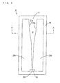
- Fig. 3 is a schematic plan view of the antenna body 6.
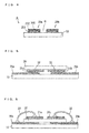
- Fig. 4 is a schematic cross sectional view of the antenna body 6. In Figs. 3 and 4 , the antenna body 6 that is not bent is shown.
- the antenna body 6 is constituted by the dielectric film 10, the pair of electrodes 20a, 20b and the semiconductor device 30.
- the dielectric film 10 is formed of resin that is made of polymer.
- One surface of the two surfaces of the dielectric film 10 facing away from each other is referred to as a main surface, and the other surface is referred to as a back surface.
- the main surface is an example of a first surface
- the back surface is an example of a second surface.
- the pair of electrodes 20a, 20b is formed on the main surface of the dielectric film 10.
- a gap that extends from one end to the other end of a set of the electrodes 20a, 20b is provided between the electrodes 20a, 20b.
- End surfaces 21 a, 21 b of the electrodes 20a, 20b that face each other are formed in a tapered shape such that the width of the gap continuously or gradually decreases from the one end to the other end of a set of the electrodes 20a, 20b.
- the gap between the electrodes 20a, 20b is referred to as a tapered slot S.
- the electrodes 20a, 20b constitute a tapered slot antenna.
- the dielectric film 10 and the electrodes 20a, 20b are formed of a flexible printed circuit board.
- the electrodes 20a, 20b are formed on the dielectric film 10 using a subtractive method, an additive method or a semi-additive method. If a below-mentioned semiconductor device 30 is appropriately mounted, the electrodes 20a, 20b may be formed on the dielectric film 10 using another method. For example, the electrodes 20a, 20b may be formed by patterning a conductive material on the dielectric film 10 using a screen printing method, an ink-jet method or the like.
- the dimension in the direction of a central axis of the tapered slot S is referred to as length, and the dimension in the direction parallel to the main surface of the dielectric film 10 and orthogonal to the central axis of the tapered slot S is referred to as width.
- the end of the tapered slot S having the maximum width is referred to as an opening end E1
- the end of the tapered slot S having the minimum width is referred to as a mount end E2.
- a direction directed from the mount end E2 toward the opening end E1 of the antenna body 6 and extends along the central axis of the tapered slot S is referred to as a central axis direction.
- the semiconductor device 30 is mounted on the ends of a set of the electrodes 20a, 20b at the mount end E2 using a flip chip mounting method or a wire bonding mounting method.
- One terminal of the semiconductor device 30 is electrically connected to the electrode 20a, and another terminal of the semiconductor device 30 is electrically connected to the electrode 20b.
- the mounting method of the semiconductor device 30 will be described below.
- the electrode 20b is to be grounded.
- Fluororesin includes PTFE, polyvinylidene fluoride, ethylene-tetrafluoroethylene copolymer, perfluoro-alkoxy fluororesin, fluorinated ethylene-propylene copolymer (tetrafluoroethylene-hexafluoropropylene copolymer) or the like.
- Polyester includes polyethylene terephthalate, polyethylene naphthalate, polybutylene terephthalate or the like.
- the dielectric film 10 is formed of polyimide.
- the thickness of the dielectric film 10 is preferably not less than 1 ⁇ m and not more than 1000 ⁇ m. In this case, the dielectric film 10 can be easily fabricated and flexibility of the dielectric film 10 can be easily ensured.
- the thickness of the dielectric film 10 is more preferably not less than 5 ⁇ m and not more than 100 ⁇ m. In this case, the dielectric film 10 can be more easily fabricated and higher flexibility of the dielectric film 10 can be easily ensured. In the present embodiment, the thickness of the dielectric film 10 is 25 ⁇ m, for example.
- the dielectric film 10 preferably has a relative permittivity of not more than 7.0, and more preferably has a relative permittivity of not more than 4.0, in a used frequency within the terahertz band.
- the radiation efficiency of an electromagnetic wave having the used frequency is sufficiently increased, and the transmission loss of the electromagnetic wave is sufficiently reduced.
- the transmission speed and the transmission distance of the electromagnetic wave having the used frequency can be sufficiently improved.
- the dielectric film 10 is formed of resin having a relative permittivity of not less than 1.2 and not more than 7.0 in the terahertz band.
- the relative permittivity of polyimide is about 3.2 in the terahertz band
- the relative permittivity of porous PTFE is about 1.2 in the terahertz band.
- the electrodes 20a, 20b may be formed of a conductive material such as metal or an alloy, and may have single layer structure or laminate structure of a plurality of layers.
- each of the electrodes 20a, 20b has the laminate structure of a copper layer 201, a nickel layer 202 and a gold layer 203.
- the thickness of the copper layer 201 is 15 ⁇ m, for example, the thickness of the nickel layer 202 is 3 ⁇ m, for example and the thickness of the gold layer 203 is 0.2 ⁇ m, for example.
- the material and the thickness of the electrodes 20a, 20b are not limited to the examples of the present embodiment.
- the laminate structure of Fig. 4 is adopted to perform the flip chip mounting by Au stud bumps and a wire bonding mounting by Au bonding wires, mentioned below.
- Formation of the nickel layer 202 and the gold layer 203 is surface processing for the copper layer 201 in a case in which the afore-mentioned mounting methods are used.
- ACFs anisotropic conductive films
- ACPs anisotropic conductive pastes
- processing appropriate for respective mounting method is selected.
- One or plurality of semiconductor devices selected from a group consisting of a resonant tunneling diode (RTD), a Schottky-barrier diode (SBD), a TUNNETT (Tunnel Transit Time) diode, an IMPATT (Impact Ionization Avalanche Transit Time) diode, a high electron mobility transistor (HEMT), a GaAs field effect transistor (FET), a GaN field effect transistor (FET) and a Heterojunction Bipolar Transistor (HBT) is used as the semiconductor device 30.
- These semiconductor devices are active elements.
- a quantum element for example, can be used as the semiconductor device 30.
- the semiconductor device 30 is a Schottky-barrier diode.
- Fig. 5 is a schematic diagram showing the mounting of the semiconductor device 30 using the flip chip mounting method.
- the semiconductor device 30 has terminals 31 a, 31 b.
- the terminals 31 a, 31 b are an anode and a cathode of a diode, for example.
- the semiconductor device 30 is positioned above the electrodes 20a, 20b such that the terminals 31 a, 31 b are directed downward, and the terminals 31 a, 31 b are bonded to the electrodes 20a, 20b using Au stud bumps 32, respectively.
- Fig. 6 is a schematic diagram showing the mounting of the semiconductor device 30 using the wire bonding mounting method. As shown in Fig. 6 , the semiconductor device 30 is positioned on the electrodes 20a, 20b such that the terminals 31 a, 31 b are directed upward, and the terminals 31 a, 31 b are connected to the electrodes 20a, 20b respectively using Au bonding wires 33.
- an area from the opening end E1 of the taper slot S to the mount portion for the semiconductor device 30 functions as a transmitter/receiver that transmits or receives the electromagnetic wave.
- the frequency of the electromagnetic wave transmitted or received by the antenna body 6 is determined by the width of the taper slot S and an effective permittivity of the tapered slot S.
- the effective permittivity of the tapered slot S is calculated based on the relative permittivity of the air between the electrodes 20a, 20b, and the relative permittivity and the thickness of the dielectric film 10.
- the length of the tapered slot S is preferably not less than 0.5 mm and not more than 30 mm. A mount area for the semiconductor device 30 can be ensured when the length of the tapered slot S is not less than 0.5 mm. Further, the length of the tapered slot S is preferably not more than 30 mm on the basis of 10 wavelengths.
- Fig. 7 is a schematic plan view showing the reception operation of the antenna body 6 according to the present embodiment.
- an electromagnetic wave RW includes a digital intensity modulated signal wave having a frequency (0.3 THz, for example) in the terahertz band and a signal wave having a frequency (1 GHz, for example) in a gigahertz band.
- the electromagnetic wave RW is received in the tapered slot S of the antenna body 6.
- an electric current having a frequency component in the terahertz band flows in the electrodes 20a, 20b.
- the semiconductor device 30 performs detection and rectification.
- a signal SG having a frequency (1 GHz, for example) in the gigahertz band is output from the semiconductor device 30.
- Fig. 8 is a schematic plan view showing the transmission operation of the antenna body 6 according to the present embodiment.
- the signal SG having a frequency (1 GHz, for example) in the gigahertz band is input to the semiconductor device 30.
- the semiconductor device 30 performs oscillation.
- the electromagnetic wave RW is transmitted from the tapered slot S of the antenna body 6.
- the electromagnetic wave RW includes the digital intensity modulated signal wave having a frequency (0.3 THz, for example) in the terahertz band and a signal wave having a frequency (1 GHz, for example) in the gigahertz band.
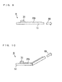
- Fig. 9 is a schematic side view for explaining the directivity of the antenna body 6 according to the present embodiment.
- the antenna body 6 radiates a carrier wave modulated by the signal wave as the electromagnetic wave RW.
- the electromagnetic wave RW is not attracted to the dielectric film 10. Therefore, the electromagnetic wave RW advances in the central axis direction of the antenna body 6.
- Fig. 10 is a schematic side view for explaining the change in directivity of the antenna body 6 according to the present embodiment.
- the dielectric film 10 of the antenna body 6 is flexible. Therefore, the antenna body 6 can be bent along an axis that intersects with the central axis direction. Thus, as shown in Fig. 10 , the radiation direction of the electromagnetic wave RW can be changed to any direction.
- the back surface of the dielectric film 10 is attached to the support surfaces 7a, 7b of the support body 5 with the antenna body 6 being bent along an axis vertical to the central axis direction.
- the radiation direction of the electromagnetic wave RW can be fixed to a desired direction.
- material having a lower relative permittivity is used as the material for the support body 5, whereby the radiation direction of the electromagnetic wave RW can be more accurately adjusted.
- Characteristics of the antenna body 6 according to the present embodiment were evaluated by the simulation and an experiment.
- Fig. 11 is a schematic plan view for explaining the dimensions of the antenna body 6 used for the simulation and the experiment.
- the distance WO between the outer end edges of the electrodes 20a, 20b in the width direction is 2.83 mm.
- the width W1 of the tapered slot S at the opening end E1 is 1.11 mm.
- the widths W2, W3 of the tapered slot S at positions P1, P2 between the opening end E1 and the mount end E2 are 0.88 mm and 0.36 mm, respectively.
- the length L1 between the opening end E1 and the position P1 is 1.49 mm
- the length L2 between the position P1 and the position P2 is 1.49 mm.
- the length L3 between the position P2 and the mount end E2 is 3.73 mm.
- the width of the tapered slot S at the mount end E2 is 50 ⁇ m.
- the radiation efficiency at 300 GHz were found by the electric field simulation using polyimide, porous PTFE and InP that is a semiconductor material as the material for the dielectric film 10, provided that the thickness of the dielectric film 10 is 25 ⁇ m, 100 ⁇ m, 250 ⁇ m, 500 ⁇ m and 1000 ⁇ m.
- the value of the relative permittivity of polyimide was considered as 3.2
- the value of the relative permittivity of porous PTFE was considered as 1.6
- the value of the relative permittivity of InP was considered as 12.4.
- the supply power is the electric power supplied to the antenna body 6.
- the radiation power is the electric power radiated from the antenna body 6. In the present simulation, the supply power is 1 mW.
- Fig. 12 is a diagram showing the simulation results of the relation between the thickness of the dielectric film 10 and the radiation efficiency at 300 GHz.
- the ordinate of Fig. 12 indicates the radiation efficiency, and the abscissa indicates the thickness of the dielectric film 10.
- the radiation efficiency of substantially 100% is obtained with the thickness of the dielectric film 10 being in a range from 25 ⁇ m to 1000 ⁇ m.
- the radiation efficiency of substantially not less than 75% is obtained with the thickness of the dielectric film 10 being in a range from 25 ⁇ m to 1000 ⁇ m.
- InP is used as the material for the dielectric film 10
- the radiation efficiency sharply decreases as the thickness of the dielectric film 10 increases from 25 ⁇ m to 250 ⁇ m.
- the thickness of the dielectric film 10 is more than 500 ⁇ m, the radiation efficiency decreases to approximately 20%.
- the radiation efficiency is high in a wide range of the thickness of the dielectric film 10, as compared to a case in which a semiconductor material is used as the material for the dielectric film 10. It is found that when porous resin is used in particular, the radiation efficiency is high regardless of the thickness of the dielectric film 10.
- the thickness of the semiconductor substrate is preferably at least 200 ⁇ m. If the thickness of the semiconductor substrate is less than 200 ⁇ m, it is difficult to handle the semiconductor device 30, and the semiconductor substrate is easy to be damaged. From the above results, if the thickness of the semiconductor substrate is not less than 200 ⁇ m, the radiation efficiency decreases to not more than about 30%.
- the radiation efficiency at 300 GHz was found by the electromagnetic field simulation, provided that the relative permittivity of the dielectric film 10 is 1.8, 2.0, 2.2, 2.4, 2.6, 2.8 and 3.0.
- Fig. 13 is a diagram showing the simulation results of the relation between the relative permittivity of the dielectric film 10 and the radiation efficiency at 300 GHz.
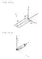
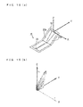
- Figs. 14(a) and 14(b) are diagrams showing the results of the three-dimensional electromagnetic field simulation obtained when the antenna module 1 is not bent.
- Figs. 15(a) and 15(b) are diagrams showing the results of the three-dimensional electromagnetic field simulation obtained when the antenna module 1 is bent.
- Figs. 14(a) and 15(a) are diagrams for explaining the definition of the directions of the antenna module 1
- Figs. 14(b) and 15(b) are diagrams showing the radiation characteristics (directivity) of the antenna module 1.
- the central axis direction of the antenna module 1 is referred to as the Y direction
- a direction parallel to the main surface of the dielectric film 10 and orthogonal to the Y direction is referred to as the X direction
- a direction vertical to the main surface of the dielectric film 10 is referred to as the Z direction.
- the electromagnetic wave is radiated in the Y direction as shown in Fig. 14(b) .
- the electromagnetic wave is radiated obliquely upward by 45° with respect to the Y direction in the YZ plane as shown in Fig. 15(b) .
- Fig. 16 is a schematic diagram for explaining the definition of the reception angle of the antenna module 1 in the simulation.
- the central axis direction of the antenna module 1 is considered as 0°.
- a plane parallel to the main surface of the dielectric film 10 is referred to as a parallel plane, and a plane vertical to the main surface of the dielectric film 10 is referred to as a vertical plane.
- an angle that is formed in the vertical plane with respect to the central axis direction is referred to as an elevation angle ⁇ 1 .
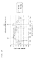
- Fig. 17 is a diagram showing the calculation results of the antenna gain obtained when the antenna module 1 is not bent and when the antenna module 1 is bent.
- the ordinate of Fig. 17 indicates the antenna gain [dBi], and the abscissa indicates the elevation angle ⁇ 1 .
- the calculation results of the antenna gain of the antenna module 1 that is not bent (un-bent model) is indicated by the dotted line, and the calculation results of the antenna gain of the antenna module 1 that is bent (45° bent model) is indicated by the solid line.
- the direction of the directivity of the antenna module 1 can be arbitrarily set by bending the antenna module 1.
- the dielectric film 10 is formed of resin to be bendable.
- the orientations of the electrodes 20a, 20b can be easily changed, and the receipt direction or the transmission direction of the electromagnetic wave can be easily adjusted.
- the bent dielectric film 10 is supported by the support body 5, the shape-retaining property of the dielectric film 10 is ensured.
- the radiation direction of the electromagnetic wave can be fixed to an adjusted direction. Therefore, even if the degree of freedom in arranging the antenna module 1 is limited, the receipt direction or the transmission direction of the electromagnetic wave can be set to a desired direction.
- the dielectric film 10 is formed of resin, the effective permittivity of the tapered slot S is reduced.
- the electromagnetic wave radiated from the electrodes 20a, 20b and the electromagnetic wave received by the electrodes 20a, 20b are less likely attracted to the dielectric film 10. Therefore, the electromagnetic wave can be efficiently radiated, and the better directivity of the antenna module is obtained.
- the effective permittivity of the tapered slot S is low, the transmission loss of the electromagnetic wave is reduced. Thus, the transmission speed and the transmission distance can be improved.
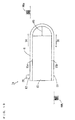
- Fig. 18 is an external perspective view of the antenna module according to the second embodiment of the present invention.
- Fig. 19 is a schematic side view of the antenna module of Fig. 18 .
- an antenna module 1 a of Figs. 18 and 19 difference from the antenna module 1 of Figs. 1 and 2 will be described.
- the antenna module 1a of Figs. 18 and 19 includes a rectangular parallelepiped support body 15 instead of the support body 5 of Figs. 1 and 2 .
- the antenna body 6 is attached to one surface 15a of the support body 15 and the other surface 15b parallel to the one surface 15a while being bent in a U-shape.
- the one surface 15a of the support body 15 is an example of a third surface of claim 2, and the other surface 15b is an example of a fourth surface of claim 4.
- a portion of the dielectric film 10 attached to the one surface 15a of the support body 15 is an example of a first portion of claim 2, and a portion of the dielectric film 10 attached to the other surface 15b is an example of a second portion of claim 4.
- the mount end E2 ( Fig.
- the antenna body 6 is positioned on the one surface 15a of the support body 15, and the opening end E1 ( Fig. 3 ) is positioned on the other surface 15b of the support body 15.
- the mount end E2 and the opening end E1 are positioned to face each other with the support body 15 held therebetween.
- the central axis direction D1 on the one surface 15a side of the support body 15 and the central axis direction D2 on the other surface 15b side of the support body 15 are different by 180°.
- an electromagnetic wave RWa is radiated in the central axis direction D1
- an electromagnetic wave RWb is radiated in the central axis direction D2 opposite to the central axis direction D1.
- the directivity of the antenna module 1 a is different depending on the material for the support body 15 and the radius of curvature (hereinafter referred to as radius of curvature RS) at the curved portion of the antenna body 6.
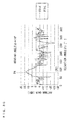
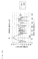
- the relation between the material for the support body 15 and the directivity in the antenna module 1 a, and the relation between the radius of curvature RS and the directivity were found by the electromagnetic field simulation.
- Fig. 20 is a schematic diagram for explaining the definition of the transmission/receipt angle of the antenna module 1 a in the simulation.
- a plane that is vertical to the one surface 15a and the other surface 15b of the support body 15, and passes in the central axis directions D1, D2 of the antenna body 6 is referred to as a vertical plane.
- a direction that is vertical to the central axis directions D1, D2 and is directed from the other surface 15b to the one surface 15a of the support body 15 is referred to as a reference direction D3.
- an angle formed with the reference direction D3 in the vertical plane is referred to as an elevation angle ⁇ 2 .
- the elevation angle ⁇ 2 in the central axis direction D1 is 90 degrees, and the elevation angle ⁇ 2 in the central axis direction D2 is 270 degrees.
- the change in antenna gain [dBi] due to the change in elevation angle ⁇ 2 was calculated in the simulation.
- the antenna body 6 has the dimensions explained in Fig. 11 . Further, the thickness of the copper layer 201 of Fig. 4 in the electrodes 20a, 20b is 15 ⁇ m, the thickness of the nickel layer 202 is 3 ⁇ m and the thickness of the gold layer 203 is 0.2 ⁇ m. Further, the thickness of the dielectric film 10 is 25 ⁇ m.
- Fig. 21 shows the calculation results of the antenna gain [dBi] obtained when air is arranged instead of the support body 15, that is, the support body 15 is not arranged but the antenna body 6 is simply bent in a U-shape.
- Fig. 22 shows the calculation results of the antenna gain [dBi] obtained when porous PTFE is used as the material for the support body 15.
- Fig. 23 shows the calculation results of the antenna gain [dBi] obtained when PTFE that is not porous (hereinafter referred to as non-porous PTFE) is used as the material for the support body 15.
- Fig. 24 shows the calculation results of the antenna gain [dBi] obtained when FR4 is used as the material for the support body 15.
- the relative permittivity of air is 1, the relative permittivity of porous PTFE is 1.2, the relative permittivity of non-porous PTFE is 2.0 and the relative permittivity of FR4 is 4.2.
- the ordinates indicate the antenna gain [dBi], and the abscissas indicate the elevation angle ⁇ 2 . Further, the calculation results of the antenna gain obtained when the radius of curvature RS is 0.5 mm is indicated by the dotted line, and the calculation results of the antenna gain obtained when the radius of curvature RS is 1 mm is indicated by the solid line.
- the antenna gain in the central axis direction D2 is higher than the antenna gain in the central axis direction D1.
- the higher the relative permittivity of the material for the support body 15 is, the higher the antenna gain in the central axis direction D2 is.
- the relation between the magnitude of the antenna gain in the central axis direction D1 and the magnitude of the antenna gain in the central axis direction D2 is different depending on the material for the support body 15.
- the antenna gain in the central axis direction D1 is higher than the antenna gain in the central axis direction D2.
- the antenna gain in the central axis direction D2 is higher than the antenna gain in the central axis direction D1.
- the support body 15 is formed of FR4 ( Fig. 24 )
- the antenna gain in the central axis direction D1 and the antenna gain in the central axis direction D2 are substantially the same.
- the antenna gain in the central axis direction D1 is low as compared to a case in which the radius of curvature RS is 0.5 mm, and the antenna gain in the central axis direction D2 is increased.
- the antenna gain in the central axis direction D1 and the antenna gain in the central axis direction D2 can be arbitrarily adjusted by the selection of the radius of curvature RS and the material for the support body 15.
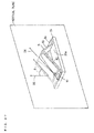
- Fig. 25 is an external perspective view of the antenna module according to the third embodiment of the present invention.
- Fig. 26 is a schematic side view of the antenna module of Fig. 25 .
- the antenna module 1b of Figs. 25 and 26 difference from the antenna module 1 of Figs. 1 and 2 will be described.
- the antenna module 1b of Figs. 25 and 26 includes a plate-shaped support body 25 instead of the support body 5 of Figs. 1 and 2 .
- the dielectric film 10 of the antenna body 6 includes portions R1, R2, R3, R4 that are arranged from the one end to the other end.
- the portion R1 is an example of a first portion of claim 2
- the portion R2 is an example of a second portion of claim 2
- the portion R3 is an example of a third portion of claim 7
- the portion R4 is an example of a fourth portion of claim 7.
- the pair of electrodes 20a, 20b and the semiconductor device 30 are provided on the main surface of the portion R2 of the dielectric film 10.
- An antenna portion 6a is constituted by the portion R2 of the dielectric film 10, the pair of electrodes 20a, 20b and the semiconductor device 30.
- the configuration of the antenna portion 6a is same as the configuration of the antenna body 6 of Fig. 3 .
- the dielectric film 10 is bent to form the valley fold at a boundary line BL1 between the portion R1 and the portion R2, is bent to form the mountain fold at a boundary line BL2 between the portion R2 and the portion R3 and is bent to form the valley fold at a boundary line BL3 between the portion R3 and the portion R4.
- the back surfaces of the portions R1, R4 are attached to one surface 25a of the support body 25.
- the portion R2 extends obliquely upward from the boundary line BL1
- the portion R3 extends obliquely downward from the boundary line BL2.
- an air layer AL is formed between the portion R2 of the dielectric film 10 and the one surface 25a of the support body 25.
- the air layer AL is an example of a space of claim 6. Because the relative permittivity of air is low as compared to the material used for the support body 25, the radiation efficiency of the electromagnetic wave having a used frequency can be sufficiently increased, and the transmission loss of the electromagnetic wave can be sufficiently reduced.
- a central axis direction D4 is parallel to the portion R2 of the dielectric film 10. Therefore, it is possible to easily adjust the radiation direction of the electromagnetic wave by adjusting an angle (hereinafter referred to as the bending angle ⁇ ) of the portion R2 of the dielectric film 10 with the one surface 25a of the support body 25.
- the antenna module 1 can be arranged in a small space.
- Fig. 27 is a schematic diagram for explaining the definition of the transmission/receipt angle of the antenna module 1b in the simulation.
- a plane that is vertical to the one surface 25a of the support body 25 and passes through the center of the mount end E2 ( Fig. 3 ) and the opening end E1 ( Fig. 3 ) of the antenna body 6 is referred to as a vertical plane.
- a direction vertical to the one surface 25a of the support body 15 is referred to as a reference direction D5.
- an angle formed with the reference direction D5 is referred to as an elevation angle ⁇ 3 .
- the bending angle ⁇ is set to 0°, 5°, 10°, 15°, 30° and 45°.
- the dimensions of the antenna portion 6a in the simulation is same as the dimensions of the antenna body 6 in the simulation of Figs. 21 to 24 .
- the dimensions of the support body 25, the dimensions of the portion R3 of the dielectric film 10, and the distance between the portion R1 and the portion R4 are appropriately set according to the bending angle ⁇ .
- Figs. 28 to 33 respectively show the calculation results of the antenna gain [dBi] obtained when the bending angle ⁇ is 0°, 5°, 10°, 15°, 30° and 45°.
- the abscissas indicate the elevation angle ⁇ 3
- the ordinates indicate the antenna gain.
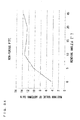
- Fig. 34 shows the relation between the bending angle ⁇ and the maximum value of the antenna gain obtained when non-porous PTFE is used as the material for the support body 25.
- Fig. 35 shows the relation between the bending angle ⁇ and the maximum value of the antenna gain obtained when FR4 is used as the material for the support body 25.
- the abscissas indicate the bending angle ⁇
- the ordinates indicate the maximum value of the antenna gain.
- the central axis direction D4 of the antenna portion 6a is indicated by the dotted line, and the elevation angle ⁇ 3 in the central axis direction D4 is indicated in brackets.
- the maximum value of the antenna gain is high as compared to a case in which the antenna portion 6a is not bent (in a case in which the bending angle ⁇ is 0°). This is considered to be because an air layer AL having a low relative permittivity is formed on the back surface side of the dielectric film 10 in a case in which the antenna 6a is bent.
- the antenna gain that is not less than 9 dBi is obtained, and when the bending angle ⁇ is not less than 10°, the antenna gain that is not less than 12 dBi is obtained.
- the maximum value of the antenna gain is higher as compared to a case in which FR4 is used.
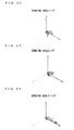
- Figs. 36 to 41 are diagrams respectively showing the results of the two-dimensional electromagnetic field simulation obtained when the bending angle ⁇ is 0°, 5°, 10°, 15°, 30° and 45°.
- Figs. 42 to 47 are diagrams respectively showing the results of the three-dimensional electromagnetic field simulation obtained when the bending angle ⁇ is 0°, 5°, 10°, 15°, 30° and 45°.
- a direction parallel to the one surface 25a of the support body 25 in the vertical plane Fig.
- X direction a direction parallel to the one surface 25a of the support body 25 and orthogonal to the X direction
- a direction vertical to the one surface 25a of the support body 25 is referred to as the Z direction.
- the bending angle ⁇ of the antenna portion 6a is changed, whereby the radiation direction of the electromagnetic wave is changed.
- the larger the bending angle ⁇ is the smaller the effect of the support body 25 on the electromagnetic wave is, so that better directivity of the electromagnetic wave is obtained.
- the bending angle ⁇ is not less than 5°, still better transmission characteristics are obtained as compared to a case in which the bending angle ⁇ is 0°.
- the bending angle ⁇ is not less than 10°, even better transmission characteristics are obtained.
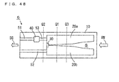
- Fig. 48 is a schematic plan view showing the modified example of the antenna body 6 according to the above-mentioned first to third embodiments.
- the antenna body 6 shown in Fig. 48 further includes signal wirings 51, 52, 53 and a low-pass filter 40 on the dielectric film 10.
- the signal wiring 51 is connected to the electrode 20a, and the signal wiring 52 is connected to the electrode 20b.
- the low-pass filter 40 is connected between the signal wiring 51 and the signal wiring 53.
- This low-pass filter 40 is formed of a meander wiring, a gold wire or the like, for example.
- the low-pass filter 40 passes only low frequency components of not more than a specific frequency (20 GHz, for example) that is a signal component in the gigahertz band.
- the electrodes 20a, 20b, the low-pass filter 40 and the signal wirings 51, 52, 53 are formed on the dielectric film 10 in the common step using the subtractive method, the additive method or the semi-additive method, or by patterning a conductive material.
- the electromagnetic wave RW includes the carrier wave having a frequency in the terahertz band and the signal wave having a frequency in the gigahertz band. This electromagnetic wave RW is received at the tapered slot S of the antenna body 6.
- a signal having a frequency in the gigahertz band is output to the signal wirings 51, 52 from the semiconductor device 30. At this time, part of a frequency component in the terahertz band may be transmitted from the electrodes 20a, 20b to the signal wirings 51, 52.
- the low-pass filter 40 blocks the frequency component in the terahertz band from passing. Thus, only the signal SG having a frequency (about 20 GHz, for example) in the gigahertz band is output to the signal wirings 51, 53.
- the antenna body 6 of Fig. 48 is used at the antenna module 1 of Figs. 1 and 2 .
- the antenna body 6 is bent along the dotted line Q1 that intersects with the electrodes 20a, 20b or the dotted line Q2 that intersects with the signal wirings 51, 52, for example, and the bent antenna body 6 is supported by the support body 5 of Figs. 1 and 2 .
- the antenna body 6 of Fig. 48 is used at the antenna module 1 a of Figs.
- the antenna body 6 is bent in a U-shape along the dotted line Q3 that intersects with the electrodes 20a, 20b, for example, the one portion that uses the dotted line Q3 as a boundary is attached to the one surface 15a of the support body 15 of Figs. 18 and 19 , and the other portion is attached to the other surface 15b of the support body 15.
- the one portion (a portion in which the electrodes 20a, 20b are not formed) of the dielectric film 10 that uses the dotted line Q2 as a boundary corresponds to the portion R1 of the dielectric film 10 of Figs. 25 and 26 , for example, and is attached to the one surface 25a of the support body 25.
- the other portion (a portion in which the electrodes 20a, 20b are formed) of the dielectric film 10 with the dotted line Q2 used as a boundary corresponds to the portion R2 of the dielectric film 10 of Figs.
- a portion of the dielectric film 10 that corresponds to the portions R3, R4 of the dielectric film 10 of Figs. 25 and 26 is provided anew, and a portion that corresponds to the portion R4 is attached to the one surface 25a of the support body 25.
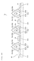
- Fig. 49 is a schematic side view of the antenna module according to the fourth embodiment. Regarding the antenna module 1c of Fig. 49 , difference from the antenna module 1 b of Figs. 25 and 26 will be described.
- the antenna module 1c of Fig. 49 includes an antenna body 60 instead of the antenna body 6.
- the antenna body 60 includes a long-sized dielectric film 10a, a plurality of pairs (six pairs in the present example) of electrodes 20a, 20b and a plurality (two in the present example) of semiconductor devices 30.
- the dielectric film 10a has a pair of fixing portions R11, a plurality (three in the present example) of electrode holding portions R12 and a plurality (two in the present example) of device mount portions R13.
- the pair of fixing portions R11 is provided at both ends of the dielectric film 10a, and the electrode holding portions R12 and the device mount portions R13 are alternately provided between the pair of fixing portions R11.
- each fixing portion R11 and each device mount portion R13 are attached to the one surface 25a of the support body 25.
- the semiconductor device 30 is mounted on the main surface of each device mount portion R13.
- Each electrode holding portion R12 includes a pair of inclination portions R12a, R12b by being bent in an inverted V-shape.
- the bending angles ⁇ 1 to ⁇ 6 of the plurality of inclination portions R12a, R12b are set to be respectively different.
- the pair of electrodes 20a, 20b is formed on each of the main surfaces of the inclination portions R12a, R12b.
- each pair of electrodes 20a, 20b forms a tapered slot S.
- Each electrode 20a, 20b is electrically connected to the terminal 31 a, 31 b ( Fig. 5 or 6 ) of any one of the semiconductor devices 30.
- the electromagnetic wave can be received or transmitted by the electrodes 20a, 20b of each inclination portion R12a, R12b.
- the electromagnetic wave can be radiated in a plurality of directions or the electromagnetic wave that arrives from a plurality of directions can be received. Further, it is possible to easily adjust the transmission/reception direction of the electromagnetic wave by adjusting the bending angle ⁇ 1 to ⁇ 6 of each inclination portion R12a, R12b.
- an air layer AL is formed between each electrode holding portion R12 in which the electrodes 20a, 20b are formed and the one surface 25a of the support body 25.
- the present invention is not limited to this.
- the electrodes 20a, 20b may be provided at the back surface of the dielectric film 10. Further, in the above-mentioned first to third embodiments, the plurality of pairs of electrodes 20a, 20b may be provided at the main surface or the back surface of the dielectric film 10.
- the semiconductor device 30 is mounted on the main surface of the dielectric film 10 in the above-mentioned first to fourth embodiments, the present invention is not limited to this.
- the semiconductor device 30 may be mounted on the back surface of the dielectric film 10. Further, in the above-mentioned first to third embodiments, the plurality of semiconductor devices 30 may be mounted on the main surface or the back surface of the dielectric film 10.
- the support bodies 5, 15, 25 are made of resin in the above-mentioned first to fourth embodiments, the present invention is not limited to this.
- the support bodies 5, 15, 25 may be formed of metal such as aluminum, copper or stainless.
- a frame-shaped support body may be provided along the outer edge of the dielectric film 10 so as not to influence the electrodes 20a, 20b.
- the present invention is not limited to these.
- the present invention is applicable to another planar antenna such as a patch antenna, a parallel slot antenna, a notch antenna or a microstrip antenna.
- the present invention can be utilized for the transmission of an electromagnetic wave having a frequency in the terahertz band.
Landscapes
- Details Of Aerials (AREA)
- Variable-Direction Aerials And Aerial Arrays (AREA)
Applications Claiming Priority (1)
| Application Number | Priority Date | Filing Date | Title |
|---|---|---|---|
| JP2013008654A JP2014140136A (ja) | 2013-01-21 | 2013-01-21 | アンテナモジュールおよびその製造方法 |
Publications (1)
| Publication Number | Publication Date |
|---|---|
| EP2757633A1 true EP2757633A1 (fr) | 2014-07-23 |
Family
ID=49920249
Family Applications (1)
| Application Number | Title | Priority Date | Filing Date |
|---|---|---|---|
| EP14151173.3A Withdrawn EP2757633A1 (fr) | 2013-01-21 | 2014-01-14 | Module d'antenne et son procédé de fabrication |
Country Status (4)
| Country | Link |
|---|---|
| US (1) | US20140203994A1 (fr) |
| EP (1) | EP2757633A1 (fr) |
| JP (1) | JP2014140136A (fr) |
| CN (1) | CN103943951A (fr) |
Cited By (2)
| Publication number | Priority date | Publication date | Assignee | Title |
|---|---|---|---|---|
| WO2018202304A1 (fr) * | 2017-05-04 | 2018-11-08 | Huawei Technologies Co., Ltd. | Élément rayonnant à double polarisation et antenne |
| US11342688B2 (en) | 2017-09-12 | 2022-05-24 | Huawei Technologies Co., Ltd. | Dual-polarized radiating element and antenna |
Families Citing this family (4)
| Publication number | Priority date | Publication date | Assignee | Title |
|---|---|---|---|---|
| JP6039472B2 (ja) * | 2013-03-15 | 2016-12-07 | 日東電工株式会社 | アンテナモジュールおよびその製造方法 |
| DE102014014860B3 (de) * | 2014-10-06 | 2015-09-17 | Audi Ag | Radarsensoranordnung und Kraftfahrzeug |
| KR102067708B1 (ko) * | 2018-06-26 | 2020-01-20 | 엘지전자 주식회사 | 안테나 모듈 및 그의 제조 방법과 안테나 모듈을 갖는 전자 기기 |
| CN119148234A (zh) * | 2023-05-09 | 2024-12-17 | 深圳市小安智慧科技有限公司 | 一种非线性节点检测模组、安检装置和安检门 |
Citations (7)
| Publication number | Priority date | Publication date | Assignee | Title |
|---|---|---|---|---|
| US20050264448A1 (en) * | 2004-05-28 | 2005-12-01 | Cox Gerald A | Radiator structures |
| US20060061508A1 (en) * | 2004-09-17 | 2006-03-23 | Fujitsu Component Limited | Antenna apparatus |
| US20060092086A1 (en) * | 2004-10-29 | 2006-05-04 | Franson Steven J | Tapered slot feed for an automotive radar antenna |
| WO2009024813A1 (fr) * | 2007-08-22 | 2009-02-26 | Bae Systems Plc | Antenne à lentille déployable |
| JP2010057161A (ja) | 2008-07-29 | 2010-03-11 | Rohm Co Ltd | テラヘルツ発振素子 |
| EP2408066A1 (fr) * | 2010-07-14 | 2012-01-18 | Raytheon Company | Systèmes et procédés pour exciter des radiateurs à longue rainure d'une antenne RF |
| EP2731195A1 (fr) * | 2012-11-12 | 2014-05-14 | Nitto Denko Corporation | Module d'antenne |
Family Cites Families (1)
| Publication number | Priority date | Publication date | Assignee | Title |
|---|---|---|---|---|
| US5070339A (en) * | 1989-12-21 | 1991-12-03 | Hughes Aircraft Company | Tapered-element array antenna with plural octave bandwidth |
-
2013
- 2013-01-21 JP JP2013008654A patent/JP2014140136A/ja active Pending
-
2014
- 2014-01-14 EP EP14151173.3A patent/EP2757633A1/fr not_active Withdrawn
- 2014-01-15 US US14/155,882 patent/US20140203994A1/en not_active Abandoned
- 2014-01-21 CN CN201410027337.1A patent/CN103943951A/zh active Pending
Patent Citations (7)
| Publication number | Priority date | Publication date | Assignee | Title |
|---|---|---|---|---|
| US20050264448A1 (en) * | 2004-05-28 | 2005-12-01 | Cox Gerald A | Radiator structures |
| US20060061508A1 (en) * | 2004-09-17 | 2006-03-23 | Fujitsu Component Limited | Antenna apparatus |
| US20060092086A1 (en) * | 2004-10-29 | 2006-05-04 | Franson Steven J | Tapered slot feed for an automotive radar antenna |
| WO2009024813A1 (fr) * | 2007-08-22 | 2009-02-26 | Bae Systems Plc | Antenne à lentille déployable |
| JP2010057161A (ja) | 2008-07-29 | 2010-03-11 | Rohm Co Ltd | テラヘルツ発振素子 |
| EP2408066A1 (fr) * | 2010-07-14 | 2012-01-18 | Raytheon Company | Systèmes et procédés pour exciter des radiateurs à longue rainure d'une antenne RF |
| EP2731195A1 (fr) * | 2012-11-12 | 2014-05-14 | Nitto Denko Corporation | Module d'antenne |
Cited By (3)
| Publication number | Priority date | Publication date | Assignee | Title |
|---|---|---|---|---|
| WO2018202304A1 (fr) * | 2017-05-04 | 2018-11-08 | Huawei Technologies Co., Ltd. | Élément rayonnant à double polarisation et antenne |
| US11205859B2 (en) | 2017-05-04 | 2021-12-21 | Huawei Technologies Co., Ltd. | Dual-polarized radiating element and antenna |
| US11342688B2 (en) | 2017-09-12 | 2022-05-24 | Huawei Technologies Co., Ltd. | Dual-polarized radiating element and antenna |
Also Published As
| Publication number | Publication date |
|---|---|
| CN103943951A (zh) | 2014-07-23 |
| JP2014140136A (ja) | 2014-07-31 |
| US20140203994A1 (en) | 2014-07-24 |
Similar Documents
| Publication | Publication Date | Title |
|---|---|---|
| EP2731195A1 (fr) | Module d'antenne | |
| EP2765651A1 (fr) | Module d'antenne et son procédé de fabrication | |
| US8164535B2 (en) | Coplanar waveguide FED planar log-periodic antenna | |
| US20140203994A1 (en) | Antenna module and method for manufacturing the same | |
| US8564492B2 (en) | Horn antenna including integrated electronics and associated method | |
| US11870144B2 (en) | Antenna, wireless communication module, and wireless communication device | |
| US9553370B2 (en) | Antenna module and method for manufacturing the same | |
| US20100321273A1 (en) | Wideband antenna and clothing and articles using the same | |
| CN104185926B (zh) | 天线装置 | |
| WO2019208453A1 (fr) | Antenne de véhicule, verre à vitre ayant une antenne de véhicule et système d'antenne | |
| US20220102859A1 (en) | High gain and fan beam antenna structures and associated antenna-in-package | |
| GB2544415A (en) | Flexible polymer antenna with multiple ground resonators | |
| US20210028548A1 (en) | Antenna apparatus, and manufacturing method | |
| CN108767436B (zh) | 天线及无人飞行器 | |
| US9755307B2 (en) | Antenna structure and wireless communication device employing same | |
| CN108767435A (zh) | 天线及无人飞行器 | |
| US20210328335A1 (en) | Antenna, array antenna, and wireless communication device | |
| CN208637583U (zh) | 天线及无人飞行器 | |
| EP3996201A1 (fr) | Circuit de conversion de ligne microruban coaxiale | |
| CN110767982A (zh) | 天线结构及具有该天线结构的电子装置 | |
| US20140118207A1 (en) | Antenna assembly | |
| JP7863803B2 (ja) | 広帯域型アンテナ | |
| JP2004173143A (ja) | アンテナと通信ケーブルの接続部構造 | |
| US20220255180A1 (en) | Electronic device | |
| JP5543795B2 (ja) | アンテナ装置及びそれを備えたrfidタグ |
Legal Events
| Date | Code | Title | Description |
|---|---|---|---|
| PUAI | Public reference made under article 153(3) epc to a published international application that has entered the european phase |
Free format text: ORIGINAL CODE: 0009012 |
|
| 17P | Request for examination filed |
Effective date: 20140114 |
|
| AK | Designated contracting states |
Kind code of ref document: A1 Designated state(s): AL AT BE BG CH CY CZ DE DK EE ES FI FR GB GR HR HU IE IS IT LI LT LU LV MC MK MT NL NO PL PT RO RS SE SI SK SM TR |
|
| AX | Request for extension of the european patent |
Extension state: BA ME |
|
| R17P | Request for examination filed (corrected) |
Effective date: 20150122 |
|
| RBV | Designated contracting states (corrected) |
Designated state(s): AL AT BE BG CH CY CZ DE DK EE ES FI FR GB GR HR HU IE IS IT LI LT LU LV MC MK MT NL NO PL PT RO RS SE SI SK SM TR |
|
| STAA | Information on the status of an ep patent application or granted ep patent |
Free format text: STATUS: THE APPLICATION HAS BEEN WITHDRAWN |
|
| 18W | Application withdrawn |
Effective date: 20150522 |