EP2763008A2 - Agencement de capteur capacitif et procédé de mesure capacitive avec compensation des capacités parasites - Google Patents
Agencement de capteur capacitif et procédé de mesure capacitive avec compensation des capacités parasites Download PDFInfo
- Publication number
- EP2763008A2 EP2763008A2 EP14153453.7A EP14153453A EP2763008A2 EP 2763008 A2 EP2763008 A2 EP 2763008A2 EP 14153453 A EP14153453 A EP 14153453A EP 2763008 A2 EP2763008 A2 EP 2763008A2
- Authority
- EP
- European Patent Office
- Prior art keywords
- amplifier
- capacitance
- sensor electrode
- sensor
- electrode
- Prior art date
- Legal status (The legal status is an assumption and is not a legal conclusion. Google has not performed a legal analysis and makes no representation as to the accuracy of the status listed.)
- Withdrawn
Links
Images
Classifications
-
- G—PHYSICS
- G06—COMPUTING OR CALCULATING; COUNTING
- G06F—ELECTRIC DIGITAL DATA PROCESSING
- G06F3/00—Input arrangements for transferring data to be processed into a form capable of being handled by the computer; Output arrangements for transferring data from processing unit to output unit, e.g. interface arrangements
- G06F3/01—Input arrangements or combined input and output arrangements for interaction between user and computer
- G06F3/03—Arrangements for converting the position or the displacement of a member into a coded form
- G06F3/041—Digitisers, e.g. for touch screens or touch pads, characterised by the transducing means
- G06F3/0416—Control or interface arrangements specially adapted for digitisers
- G06F3/0418—Control or interface arrangements specially adapted for digitisers for error correction or compensation, e.g. based on parallax, calibration or alignment
- G06F3/04182—Filtering of noise external to the device and not generated by digitiser components
-
- G—PHYSICS
- G06—COMPUTING OR CALCULATING; COUNTING
- G06F—ELECTRIC DIGITAL DATA PROCESSING
- G06F3/00—Input arrangements for transferring data to be processed into a form capable of being handled by the computer; Output arrangements for transferring data from processing unit to output unit, e.g. interface arrangements
- G06F3/01—Input arrangements or combined input and output arrangements for interaction between user and computer
- G06F3/03—Arrangements for converting the position or the displacement of a member into a coded form
- G06F3/041—Digitisers, e.g. for touch screens or touch pads, characterised by the transducing means
- G06F3/0416—Control or interface arrangements specially adapted for digitisers
-
- H—ELECTRICITY
- H03—ELECTRONIC CIRCUITRY
- H03K—PULSE TECHNIQUE
- H03K17/00—Electronic switching or gating, i.e. not by contact-making and –breaking
- H03K17/94—Electronic switching or gating, i.e. not by contact-making and –breaking characterised by the way in which the control signals are generated
- H03K17/945—Proximity switches
- H03K17/955—Proximity switches using a capacitive detector
-
- G—PHYSICS
- G06—COMPUTING OR CALCULATING; COUNTING
- G06F—ELECTRIC DIGITAL DATA PROCESSING
- G06F3/00—Input arrangements for transferring data to be processed into a form capable of being handled by the computer; Output arrangements for transferring data from processing unit to output unit, e.g. interface arrangements
- G06F3/01—Input arrangements or combined input and output arrangements for interaction between user and computer
- G06F3/03—Arrangements for converting the position or the displacement of a member into a coded form
- G06F3/041—Digitisers, e.g. for touch screens or touch pads, characterised by the transducing means
- G06F3/044—Digitisers, e.g. for touch screens or touch pads, characterised by the transducing means by capacitive means
-
- H—ELECTRICITY
- H03—ELECTRONIC CIRCUITRY
- H03K—PULSE TECHNIQUE
- H03K2217/00—Indexing scheme related to electronic switching or gating, i.e. not by contact-making or -breaking covered by H03K17/00
- H03K2217/94—Indexing scheme related to electronic switching or gating, i.e. not by contact-making or -breaking covered by H03K17/00 characterised by the way in which the control signal is generated
- H03K2217/96—Touch switches
- H03K2217/9607—Capacitive touch switches
- H03K2217/960705—Safety of capacitive touch and proximity switches, e.g. increasing reliability, fail-safe
-
- H—ELECTRICITY
- H03—ELECTRONIC CIRCUITRY
- H03K—PULSE TECHNIQUE
- H03K2217/00—Indexing scheme related to electronic switching or gating, i.e. not by contact-making or -breaking covered by H03K17/00
- H03K2217/94—Indexing scheme related to electronic switching or gating, i.e. not by contact-making or -breaking covered by H03K17/00 characterised by the way in which the control signal is generated
- H03K2217/96—Touch switches
- H03K2217/9607—Capacitive touch switches
- H03K2217/96071—Capacitive touch switches characterised by the detection principle
- H03K2217/960715—Rc-timing; e.g. measurement of variation of charge time or discharge time of the sensor
Definitions
- the present invention relates to a sensor arrangement for measuring a change in capacitance on at least one sensor electrode according to the preamble of claim 1 and to a method for measuring a change in capacitance on at least one sensor electrode.
- the changing capacitance between the sensor electrode and the electronics ground or earth is usually measured to determine whether an object is located in the vicinity of the sensor electrode and / or - when using the sensor arrangement for distance measurement - an object has approached the sensor electrode.
- a sensor arrangement for an input device such.
- a screen known in which a sensor or Nutzelektrode, the sensor electrode shielding shielding electrode and a deflection electrode are provided and an evaluation circuit
- the sensor electrode is repeatedly discharged and rechargeable to the basis of the frequency with which the discharging and charging takes place to close the size of the capacitance on the sensor electrode at an output of the evaluation circuit and to detect capacitively an input by a user on the input device.
- the deflection electrode - too referred to as field beam electrode - an electric field generated by the sensor electrode is influenced and this bundled in a relevant measuring range.
- the sensor electrode is coupled to an evaluation circuit, the at least one amplifier, for. B. a non-inverting operational amplifier, and comprises a Schmitt trigger downstream of the amplifier.
- the evaluation circuit the sensor electrode is repeatedly dischargeable and rechargeable, so that on the basis of the frequency with which the discharging and charging takes place at a Schmitt trigger downstream output on the size of the capacitance can be closed at the sensor electrode.
- the capacitance on the sensor electrode changes as a result of an object penetrating into an electric field generated by the sensor electrode.
- the frequency with which the charge and discharge of the sensor electrode takes place in a characteristic manner, so that the size of the capacitance at the sensor electrode or the change from the basic capacity can be determined based on the frequency.
- the voltage is applied across the sensor electrode and at an output of the amplifier, a compensation voltage is generated and a compensation capacity pre-defined electrical capacitance is connected to the output of the amplifier and connected in parallel to the amplifier such that the basic capacitance decreases to compensate for parasitic capacitance in the measurement.
- a compensation capacitance of predefined electrical capacitance is connected to the output of the amplifier and connected in parallel to the amplifier so that the measured basic capacitance of the sensor electrode-in particular with respect to a sensor arrangement without compensation capacitance-is reduced in order to compensate parasitic capacitances during the measurement.
- the compensation capacitance may in principle be introduced into the circuit arrangement via a cleverly selected circuit layout, so that circuit components (for example lines) which are to be provided anyway and are capacitive in the measurement function as a compensation capacitance with which a measured basic capacitance of the sensor electrode is reduced.
- a compensation capacitance may be provided via at least one discrete, preferably capacitive device, e.g. in the form of a capacitor, be provided that was specifically designed to compensate for parasitic capacitances in the manner according to the invention in the circuit arrangement.
- a compensation capacitance can thus be provided in particular by a discrete electrical component or a plurality of discrete electrical components in the sensor arrangement or an associated circuit.
- a field beam electrode in addition to the at least one sensor electrode, a field beam electrode is provided, which is designed and in that an electric field generated by the field beam electrode influences a spatial distribution of an electric field generated by the sensor electrode such that the field of the sensor electrode is bundled in a spatial measuring range.
- a field beam electrode can surround, for example, at least one sensor electrode partially or completely circumferentially, so that a bundling of the electric field generated by the sensor electrode is achieved in the area surrounding the field beam electrode.
- a sensor arrangement comprising a field beam electrode
- the field beam electrode is connected to the output of the amplifier and the field beam electrode is thus at the potential of the compensation voltage.
- the additional compensation capacitance provided for compensating parasitic capacitances is connected between the field-beam electrode and the sensor electrode.
- a low-pass filter is connected between the amplifier and the Schmitt trigger.
- the evaluation circuit is further designed and intended to be operated with a single asymmetrical supply voltage.
- the bases of the Schmitt trigger and a non-inverting amplifier are connected via a voltage divider of two equal, relatively low-resistance resistors between the supply voltage and ground.
- the latter has a second sensor electrode and / or advantageously an active integrator connected upstream of the amplifier. Both sensor electrodes form a negative feedback capacity of the integrator.
- a field beam electrode can also be here optionally between the - preferably non-inverting - amplifier and provided for compensating parasitic capacitance compensation capacity can be arranged.
- the complete evaluation circuit in particular with (non-inverting) amplifier and Schmitt trigger, is accommodated on a printed circuit board.
- the sensor arrangement is designed and provided to determine, by means of a changing capacitance at the sensor electrode, whether an object has approached the sensor electrode and / or an object is located in a surrounding area around the sensor electrode.
- a sensor arrangement according to the invention can be used in a proximity switch or sensor.
- a preferred application provides that a distance between two components of a machine tool is determined by a changing capacitance on the sensor electrode.
- a sensor arrangement according to the invention can greatly simplify the automation of machine tools and machines in general and improve an automated operation of machines in which the execution of successive process steps depends on a specific position or position of two components and this is to be detected by sensors.
- the corresponding position or position can be determined more accurately and consequently with a lower fault tolerance.
- an application in a level sensor is conceivable to capacitively determine the level of a liquid in a container by means of the sensor electrode.
- Another aspect of the present invention is a method for measuring a capacitance change on at least one sensor electrode with a basic capacitance according to claim 15.
- a method according to the invention is thus significantly characterized by the provision of a compensation capacitance which is connected to the output of the amplifier and connected in parallel thereto.
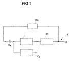
- FIG. 1 shows first schematically the basic circuit concept of a sensor arrangement according to the invention, which is designed and provided for carrying out a method according to the invention.
- a changing capacitance between a sensor electrode is measured as the measuring capacitance C X and the electronics ground or earth, for example, to determine whether there is an object in the vicinity of the sensor electrode and / or - when using the sensor arrangement for distance measurement - has approached an object of the sensor electrode SE.
- the measured capacitance C X to be measured with an evaluation circuit, here comprising a (non-inverting) amplifier I and a Schmitt trigger ST connected downstream thereof.
- the output of the Schmitt trigger ST is connected to the sensor electrode SE via a feedback RK.
- the measuring capacitance Cx is supplied, for example, via a feedback resistor with an alternating current as a clocked direct current.
- a measurement (voltage) signal U f a frequency measurable, which depends on the size of the measuring capacitance C X. If the size of the measuring capacitance C X changes, for example, due to an object located in the vicinity of the sensor electrode, the frequency changes (proportionally) between discharging and charging the measuring capacitance C X. Consequently, it is possible to determine the instantaneous magnitude of the measuring capacitance C X via the frequency of the measuring signal U f at the output A, or to determine the measuring capacitance C x .
- the illustrated sensor arrangement is preferably provided for a distance sensor or a proximity switch, for example for the automation of adjustment processes in (tool) machines.
- the change of the measuring capacitance Cx to be measured compared to a basic capacitance is usually comparatively small, the basic capacitance being understood to be the capacitance of the non-influenced sensor electrode, ie the size of the measuring capacitance Cx measured during a calibration of the sensor arrangement.
- the change in the measuring capacitance C X to be detected and evaluated lies in the range of less pF ( ⁇ 10 pF) or even less than 1 pF.
- the introduced via the evaluation circuit and with measured parasitic capacitances are very disturbing and affect the measurement effect sometimes serious.
- the amplifier I to connect a capacitive component as a compensation capacitance C P with a predefined capacitance in parallel, so that this reduces the (measured) basic capacity of the sensor electrode SE and in the measurement parasitic capacitances are compensated.
- the compensation capacitance C P is integrated between the measuring capacitance C X and the input of the amplifier I and, on the other hand, between the output of the amplifier I and the input of the Schmitt trigger ST into the sensor arrangement.
- the compensation capacitance C P can a cleverly chosen circuit layout be introduced into the circuit arrangement, so that anyway to be provided and capacitively acting in the measurement circuit parts (eg lines) act as a compensation capacitance C P , with the measured basic capacitance of the sensor electrode SE is reduced.
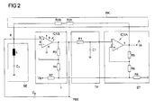
- FIG. 2 shows a concrete embodiment of the circuit concept of FIG. 1 in which the amplifier I is provided as a non-inverting amplifier with an operational amplifier IC1 / B and the Schmitt trigger ST is provided with a further operational amplifier IC1 / A. Furthermore, a low-pass filter TP with a resistor R1 and a capacitive component C1 is connected between the amplifier I and the Schmitt trigger ST in order to suppress high-frequency interference.
- the non-inverting amplifier I has in a known manner, in addition to the operational amplifier IC1 / B, two resistors R3 and R4 to form a voltage divider.
- the operational amplifier IC1 / B of the amplifier I has five connection pins 4, 5, 6, 7 and 8, the connection pin 5 being assigned to the non-inverting (positive) input of the operational amplifier IC1 / B and the connection pin 6 to the inverting (negative) input are.
- the connection pin 4 represents the ground pin, and a supply voltage U B is applied to the connection pin 8.
- the connection pin 7, in turn, represents the output of the operational amplifier IC1 / B.
- the amplifier I By means of the operational amplifier IC1 / B, the amplifier I generates at its output marked by the connection pin 7 a defined compensation voltage which is proportional to the voltage across the sensor electrode SE or above the measuring capacitance Cx is and which is increased (by a given gain factor) against this voltage.
- the Schmitt trigger ST has, in addition to the operational amplifier IC1 / A, additional resistors R5 and R6 and is constructed in a manner known per se.
- the operational amplifier IC1 / A has, in particular at a connection pin 2, the inverting input, which is connected to the low-pass filter TP and via this to the output of the operational amplifier IC1 / B of the amplifier I.
- the non-inverting (positive) input of the operational amplifier IC1 / A is assigned a terminal pin 3, to which the output signal of the operational amplifier IC1 / A is fed back.
- the output of the operational amplifier IC1 / A defines another terminal pin. 1
- the output of the Schmitt trigger ST is via a feedback RK - here having two resistors R2A and R2B - with the input of the operational amplifier IC1 / B (am Connection pin 5) connected.
- the feedback RK, the non-inverting input of the operational amplifier IC1 / B, a sensor electrode SE with the measuring capacitance C X and a connecting line leading to the compensation capacitance C P are interconnected.
- a second connecting line leading to the compensation capacitance C P is accordingly connected between the output of the amplifier I or the output of the associated operational amplifier IC1 / B and the low-pass filter TP.
- the compensation capacitance C P is further connected (in the form of a capacitor) between the sensor electrode SE and a field beam electrode FBE.
- the field beam electrode FBE bundles, such. B. from the DE 195 12 150 A1 known, an electric field generated by the sensor electrode SE in a measuring range.
- the field beam electrode FBE is arranged, for example, completely circumferentially around the sensor electrode SE.
- the compensation capacitance C P is counteracted by its arrangement between the sensor electrode SE and the field beam electrode FBE and in parallel with the amplifier I in the evaluation circuit shown with measured parasitic capacitances.
- An inductive component L of the sensor electrode SE which also serves to suppress high-frequency interference, and additional resistors R7 and R8 in the amplifier I and the Schmitt trigger ST complete the analog sensor electronics of the circuit shown.
- the bases of the Schmitt trigger ST and the non-inverting amplifier I are connected via a voltage divider of the two equal, relatively low-resistance resistors R7 and R8 between the supply voltage U B and ground.
- the circuit shown with a single asymmetrical supply voltage U B is operable.
- the charging current of the measuring capacitance C X is by definition proportional to the voltage change u CX / dt.
- the voltage u CX over the quasi-stationary measuring capacitance C X thus increases in inverse proportion to the measuring capacitance C X.
- the compensation capacitance C P acts like a reduction of a constant basic component C 0 of the measuring capacitance C X (basic capacitance):
- C x C 0 + ⁇ C with C 0 > > .DELTA.C , ⁇ C hereby symbolizes the magnification of the measuring capacitance C X z to be measured.
- B due to the approach of an object to the sensor electrode SE. This reduction of the basic capacitance C 0 increases the measuring effect.
- the non-inverting amplifier I becomes, as it were, a negative capacitance of magnitude C P ⁇ R ⁇ 3 R ⁇ 4 realized that compensates for the parasitic (positive) capacitances inherent in and measured by the electronic components used. The measuring effect is thus effectively increased.
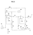
- FIG. 3 is a slightly modified embodiment of the embodiment of FIG. 2 shown, in particular instead of two resistors R2A and R2B in the feedback RK only a resistor R2A is provided. For the measurement of the frequency at the output A, an additional resistor R9 is also provided.
- the circuit construction according to the embodiment of FIG. 3 but with the circuit concept of FIG. 2 match.
- the compensation capacitance C P is in a consistent manner between the sensor electrode SE and the field beam electrode FBE are switched in such a way that they act (mathematically) like a negative capacitance and compensate parasitic capacitances during the measurement.
- a circuit layout with a single operational amplifier module is selected with the operational amplifiers IC1 / A and IC1 / B, in which the operational amplifier IC1 / B of the non-inverting amplifier I is arranged and interconnected in a special way, so that parasitic capacitances in the measurement be additionally reduced.
- the operational amplifier IC1 / B works not only with a very low input current.
- connection pin 5 On the one hand by the arrangement of the connection pin 5 at the edge of the block for the operational amplifier IC1 / B, and on the other hand due to the fact that the operational amplifier IC1 / B itself regulates a voltage difference between the positive and negative inputs to zero, parasitic capacitances are additionally avoided.
- the connection pins 5, 6, 7 and 8 for the non-inverting input, the inverting input and the output of the operational amplifier IC1 / B and for the connection to the supply voltage U B are arranged side by side and as close as possible to the sensor electrode SE, to interference or to avoid disturbing potentials.
- the connection or ground pin 4 of the operational amplifier IC1 / B is for this purpose in a preferred circuit layout spaced as far as possible to the sensor electrode SE and arranged on another side of the operational amplifier module as the connection pins 5, 6, 7 and 8.
- connection pin 5 preferably also has only short connection lines for the non-inverting (positive) input of the operational amplifier IC1 / B.
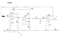
- FIG. 4 a circuit construction for a second possible embodiment of a sensor arrangement according to the invention is illustrated, in which two Sensor electrodes SE, further here represented by a single measuring capacitance C x are used in combination with a field beam electrode FBE.
- the structure of the sensor arrangement of FIG. 4 differs from the variants of the Figures 2 and 3 above all by the additional embedding of an integrator Al (also referred to as "active integrator") connected upstream of the non-inverting amplifier I.
- This additional integrator Al has, in addition to a further operational amplifier IC1 / C, an additional capacitive component C3 which is connected to the output of the operational amplifier IC1 / C of the integrator A1.
- the measuring capacitance C X and the compensation capacitance C P are respectively connected to the inverting (negative) input of the additional operational amplifier IC1 / C.
- the additional sensor electrode SE which is connected to the inverting input of the operational amplifier IC1 / C can be advantageously at least partially surrounded by another electrode, which is preferably connected to electronics ground.
- the field-beam electrode FBE can surround at least part of the first sensor electrode SE connected to the output of the operational amplifier IC1 / C.
- the electrode connected to electronic ground and the field beam electrode FBE can rotate the respective sensor electrode SE in any desired form.
- the electrode and the field beam electrode FBE the respective sensor electrode SE frame-shaped, in particular semicircular, circular or rectangular surround.
Landscapes
- Engineering & Computer Science (AREA)
- General Engineering & Computer Science (AREA)
- Theoretical Computer Science (AREA)
- Human Computer Interaction (AREA)
- Physics & Mathematics (AREA)
- General Physics & Mathematics (AREA)
- Measurement Of Resistance Or Impedance (AREA)
- Measurement Of Length, Angles, Or The Like Using Electric Or Magnetic Means (AREA)
Applications Claiming Priority (1)
| Application Number | Priority Date | Filing Date | Title |
|---|---|---|---|
| DE102013201704.9A DE102013201704A1 (de) | 2013-02-01 | 2013-02-01 | Kapazitive Sensoranordnung und kapazitives Messverfahren mit Kompensation parasitärer Kapazitäten |
Publications (2)
| Publication Number | Publication Date |
|---|---|
| EP2763008A2 true EP2763008A2 (fr) | 2014-08-06 |
| EP2763008A3 EP2763008A3 (fr) | 2017-03-08 |
Family
ID=50023475
Family Applications (1)
| Application Number | Title | Priority Date | Filing Date |
|---|---|---|---|
| EP14153453.7A Withdrawn EP2763008A3 (fr) | 2013-02-01 | 2014-01-31 | Agencement de capteur capacitif et procédé de mesure capacitive avec compensation des capacités parasites |
Country Status (2)
| Country | Link |
|---|---|
| EP (1) | EP2763008A3 (fr) |
| DE (1) | DE102013201704A1 (fr) |
Cited By (3)
| Publication number | Priority date | Publication date | Assignee | Title |
|---|---|---|---|---|
| CN109407873A (zh) * | 2017-08-17 | 2019-03-01 | 深圳指芯智能科技有限公司 | 低功耗触摸感应的检测电路、装置及方法 |
| CN111399679A (zh) * | 2020-03-11 | 2020-07-10 | 北京集创北方科技股份有限公司 | 电容检测装置 |
| CN114966223A (zh) * | 2022-05-13 | 2022-08-30 | 东南大学 | 一种消除测量电路中寄生电容的电容测量方法 |
Families Citing this family (1)
| Publication number | Priority date | Publication date | Assignee | Title |
|---|---|---|---|---|
| DE102022131053B3 (de) | 2022-11-23 | 2024-04-04 | Balluff Gmbh | Schaltungsanordnungen zur Messung wenigstens einer Kapazität |
Citations (1)
| Publication number | Priority date | Publication date | Assignee | Title |
|---|---|---|---|---|
| DE19512150A1 (de) | 1995-03-31 | 1996-10-02 | Quick Components Ltd | Eingabegerät sowie Berührungsbildschirmsystem |
Family Cites Families (8)
| Publication number | Priority date | Publication date | Assignee | Title |
|---|---|---|---|---|
| DE2744785B2 (de) * | 1977-10-05 | 1981-05-21 | Robert 7995 Neukirch Buck | Elektronischer Annäherungsschalter |
| CH652823A5 (de) * | 1980-03-26 | 1985-11-29 | Bosch Gmbh Robert | Weg-frequenz-messgroessenwandler. |
| DE3815698A1 (de) * | 1988-05-07 | 1989-11-16 | Balluff Gebhard Feinmech | Selbstpruefender, kapazitiver naeherungsschalter |
| US5166679A (en) * | 1991-06-06 | 1992-11-24 | The United States Of America As Represented By The Administrator Of The National Aeronautics & Space Administration | Driven shielding capacitive proximity sensor |
| BE1007258A3 (nl) * | 1993-07-01 | 1995-05-02 | Philips Electronics Nv | Capacitieve sensorschakeling. |
| EP1106981A3 (fr) * | 1999-12-09 | 2002-07-24 | Texas Instruments Incorporated | Transducteur capacitif |
| CH700376A2 (de) * | 2009-02-11 | 2010-08-13 | Baumer Innotec Ag | Kapazitiver Sensor und Verfahren zur kapazitiven Erfassung eines Objektabstandes. |
| JP5639655B2 (ja) * | 2010-09-28 | 2014-12-10 | 株式会社フジクラ | 静電容量センサ |
-
2013
- 2013-02-01 DE DE102013201704.9A patent/DE102013201704A1/de not_active Ceased
-
2014
- 2014-01-31 EP EP14153453.7A patent/EP2763008A3/fr not_active Withdrawn
Patent Citations (1)
| Publication number | Priority date | Publication date | Assignee | Title |
|---|---|---|---|---|
| DE19512150A1 (de) | 1995-03-31 | 1996-10-02 | Quick Components Ltd | Eingabegerät sowie Berührungsbildschirmsystem |
Cited By (5)
| Publication number | Priority date | Publication date | Assignee | Title |
|---|---|---|---|---|
| CN109407873A (zh) * | 2017-08-17 | 2019-03-01 | 深圳指芯智能科技有限公司 | 低功耗触摸感应的检测电路、装置及方法 |
| CN109407873B (zh) * | 2017-08-17 | 2024-06-07 | 江西指芯智能科技有限公司 | 低功耗触摸感应的检测电路、装置及方法 |
| CN111399679A (zh) * | 2020-03-11 | 2020-07-10 | 北京集创北方科技股份有限公司 | 电容检测装置 |
| US12092671B2 (en) | 2020-03-11 | 2024-09-17 | Chipone Technology (Beijing) Co., Ltd. | Capacitance measurement apparatus |
| CN114966223A (zh) * | 2022-05-13 | 2022-08-30 | 东南大学 | 一种消除测量电路中寄生电容的电容测量方法 |
Also Published As
| Publication number | Publication date |
|---|---|
| DE102013201704A1 (de) | 2014-08-07 |
| EP2763008A3 (fr) | 2017-03-08 |
Similar Documents
| Publication | Publication Date | Title |
|---|---|---|
| EP3152530B1 (fr) | Procédé et dispositif de surveillance du niveau d'un milieu dans un récipient | |
| EP2100101B1 (fr) | Système pour mesurer une grandeur physique | |
| EP2668512B1 (fr) | Procédé de détermination sans contact d'un potentiel électrique d'un objet au moyen de deux valeurs de flux électrique différentes et dispositif associé | |
| DE102013005939A1 (de) | Messwiderstand und entsprechendes Messverfahren | |
| DE102011078334A1 (de) | Verfahren und System zum Kalibrieren eines Shunt-Widerstands | |
| DE112013006074T5 (de) | Kapazitiver Sensor, der dafür ausgelegt ist, ein Heizelement als Antennenelektrode zu verwenden | |
| DE4447295A1 (de) | Verfahren und Vorrichtung zur Bestimmung einer jeweiligen örtlichen Position eines Körpers durch kapazitive Abtastung | |
| EP3293499B1 (fr) | Procédé de fonctionnement d'un débitmètre magnétique inductif et débitmètre magnétique inductif | |
| DE102014117821A1 (de) | Sensorsystem für ein Lenkrad eines Kraftfahrzeugs, Lenkrad mit einem solchen Sensorsystem und Verfahren zum Betrieb eines solchen Sensorsystems | |
| EP2763008A2 (fr) | Agencement de capteur capacitif et procédé de mesure capacitive avec compensation des capacités parasites | |
| EP3074726B1 (fr) | Palpeur de mesure inductif et procédé permettant de faire fonctionner un palpeur de mesure inductif | |
| EP0711978B1 (fr) | Procédé et dispositif pour déterminer la position réelle d'un objet par balayage capacitif | |
| EP3764054B1 (fr) | Agencement de capteur permettant de détecter une déviation d'une fil électrode | |
| EP1034412B1 (fr) | Mesure de distance capacitive a l'aide d'une electrode de mesure non ideale | |
| DE102019213127A1 (de) | Vorrichtung für einen nichtkontaktiven sensor mit esd-schutzstruktur | |
| DE102018106493A1 (de) | Schutzschaltung für oszilloskopmesskanal | |
| DE102013224235B4 (de) | Sensorsystem zur kapazitiven Abstandsmessung | |
| DE102008064544B4 (de) | Positions-/Wegmesssystem und Verfahren zur Bestimmung der Position eines Gebers | |
| DE102021121869A1 (de) | Verfahren zur Kalibrierung und/oder Linearisierung eines Positionssensors; Positionssensor; Hinterachslenkung; Fahrzeug; Computerprogramm | |
| DE19850290C2 (de) | Schaltungsanordnung zur linearen kapazitiven Messung | |
| EP3070436B1 (fr) | Systeme de mesure de position comprenant des moyens d'etalonnage | |
| DE102022131053B3 (de) | Schaltungsanordnungen zur Messung wenigstens einer Kapazität | |
| DE102010047198A1 (de) | Abstandmesseinrichtung für Bearbeitungswerkzeuge | |
| EP3444575B1 (fr) | Dispositif capteur destiné à la mesure potentiometrique d'une hauteur de niveau de remplissage dans un recipient | |
| EP2872903B1 (fr) | Appareil de mesure, utilisation de l'appareil de mesure et procédé pour mesurer une tension alternative |
Legal Events
| Date | Code | Title | Description |
|---|---|---|---|
| PUAI | Public reference made under article 153(3) epc to a published international application that has entered the european phase |
Free format text: ORIGINAL CODE: 0009012 |
|
| 17P | Request for examination filed |
Effective date: 20140131 |
|
| AK | Designated contracting states |
Kind code of ref document: A2 Designated state(s): AL AT BE BG CH CY CZ DE DK EE ES FI FR GB GR HR HU IE IS IT LI LT LU LV MC MK MT NL NO PL PT RO RS SE SI SK SM TR |
|
| AX | Request for extension of the european patent |
Extension state: BA ME |
|
| PUAL | Search report despatched |
Free format text: ORIGINAL CODE: 0009013 |
|
| AK | Designated contracting states |
Kind code of ref document: A3 Designated state(s): AL AT BE BG CH CY CZ DE DK EE ES FI FR GB GR HR HU IE IS IT LI LT LU LV MC MK MT NL NO PL PT RO RS SE SI SK SM TR |
|
| AX | Request for extension of the european patent |
Extension state: BA ME |
|
| RIC1 | Information provided on ipc code assigned before grant |
Ipc: G06F 3/044 20060101ALI20170131BHEP Ipc: G06F 3/041 20060101AFI20170131BHEP Ipc: H03K 17/955 20060101ALI20170131BHEP |
|
| STAA | Information on the status of an ep patent application or granted ep patent |
Free format text: STATUS: THE APPLICATION IS DEEMED TO BE WITHDRAWN |
|
| 18D | Application deemed to be withdrawn |
Effective date: 20170909 |