EP2765536A1 - Verfahren zur Verbindung eines Mikroschaltkreises mit leitenden Zonen, die in einem Träger zugänglich sind - Google Patents
Verfahren zur Verbindung eines Mikroschaltkreises mit leitenden Zonen, die in einem Träger zugänglich sind Download PDFInfo
- Publication number
- EP2765536A1 EP2765536A1 EP13305150.8A EP13305150A EP2765536A1 EP 2765536 A1 EP2765536 A1 EP 2765536A1 EP 13305150 A EP13305150 A EP 13305150A EP 2765536 A1 EP2765536 A1 EP 2765536A1
- Authority
- EP
- European Patent Office
- Prior art keywords
- connection
- micromodule
- portions
- periphery
- cavity
- Prior art date
- Legal status (The legal status is an assumption and is not a legal conclusion. Google has not performed a legal analysis and makes no representation as to the accuracy of the status listed.)
- Withdrawn
Links
Images

Classifications
-
- G—PHYSICS
- G06—COMPUTING OR CALCULATING; COUNTING
- G06K—GRAPHICAL DATA READING; PRESENTATION OF DATA; RECORD CARRIERS; HANDLING RECORD CARRIERS
- G06K19/00—Record carriers for use with machines and with at least a part designed to carry digital markings
- G06K19/06—Record carriers for use with machines and with at least a part designed to carry digital markings characterised by the kind of the digital marking, e.g. shape, nature, code
- G06K19/067—Record carriers with conductive marks, printed circuits or semiconductor circuit elements, e.g. credit or identity cards also with resonating or responding marks without active components
- G06K19/07—Record carriers with conductive marks, printed circuits or semiconductor circuit elements, e.g. credit or identity cards also with resonating or responding marks without active components with integrated circuit chips
- G06K19/077—Constructional details, e.g. mounting of circuits in the carrier
- G06K19/07745—Mounting details of integrated circuit chips
- G06K19/07747—Mounting details of integrated circuit chips at least one of the integrated circuit chips being mounted as a module
-
- G—PHYSICS
- G06—COMPUTING OR CALCULATING; COUNTING
- G06K—GRAPHICAL DATA READING; PRESENTATION OF DATA; RECORD CARRIERS; HANDLING RECORD CARRIERS
- G06K19/00—Record carriers for use with machines and with at least a part designed to carry digital markings
- G06K19/06—Record carriers for use with machines and with at least a part designed to carry digital markings characterised by the kind of the digital marking, e.g. shape, nature, code
- G06K19/067—Record carriers with conductive marks, printed circuits or semiconductor circuit elements, e.g. credit or identity cards also with resonating or responding marks without active components
- G06K19/07—Record carriers with conductive marks, printed circuits or semiconductor circuit elements, e.g. credit or identity cards also with resonating or responding marks without active components with integrated circuit chips
- G06K19/077—Constructional details, e.g. mounting of circuits in the carrier
- G06K19/07749—Constructional details, e.g. mounting of circuits in the carrier the record carrier being capable of non-contact communication, e.g. constructional details of the antenna of a non-contact smart card
- G06K19/07766—Constructional details, e.g. mounting of circuits in the carrier the record carrier being capable of non-contact communication, e.g. constructional details of the antenna of a non-contact smart card comprising at least a second communication arrangement in addition to a first non-contact communication arrangement
- G06K19/07769—Constructional details, e.g. mounting of circuits in the carrier the record carrier being capable of non-contact communication, e.g. constructional details of the antenna of a non-contact smart card comprising at least a second communication arrangement in addition to a first non-contact communication arrangement the further communication means being a galvanic interface, e.g. hybrid or mixed smart cards having a contact and a non-contact interface
-
- H—ELECTRICITY
- H10—SEMICONDUCTOR DEVICES; ELECTRIC SOLID-STATE DEVICES NOT OTHERWISE PROVIDED FOR
- H10W—GENERIC PACKAGES, INTERCONNECTIONS, CONNECTORS OR OTHER CONSTRUCTIONAL DETAILS OF DEVICES COVERED BY CLASS H10
- H10W72/00—Interconnections or connectors in packages
- H10W72/851—Dispositions of multiple connectors or interconnections
- H10W72/874—On different surfaces
- H10W72/884—Die-attach connectors and bond wires
-
- H—ELECTRICITY
- H10—SEMICONDUCTOR DEVICES; ELECTRIC SOLID-STATE DEVICES NOT OTHERWISE PROVIDED FOR
- H10W—GENERIC PACKAGES, INTERCONNECTIONS, CONNECTORS OR OTHER CONSTRUCTIONAL DETAILS OF DEVICES COVERED BY CLASS H10
- H10W74/00—Encapsulations, e.g. protective coatings
-
- H—ELECTRICITY
- H10—SEMICONDUCTOR DEVICES; ELECTRIC SOLID-STATE DEVICES NOT OTHERWISE PROVIDED FOR
- H10W—GENERIC PACKAGES, INTERCONNECTIONS, CONNECTORS OR OTHER CONSTRUCTIONAL DETAILS OF DEVICES COVERED BY CLASS H10
- H10W90/00—Package configurations
- H10W90/701—Package configurations characterised by the relative positions of pads or connectors relative to package parts
- H10W90/751—Package configurations characterised by the relative positions of pads or connectors relative to package parts of bond wires
- H10W90/754—Package configurations characterised by the relative positions of pads or connectors relative to package parts of bond wires between a chip and a stacked insulating package substrate, interposer or RDL
Definitions
- the invention relates to a method for connecting a microcircuit to accessible conductive zones or tracks in a support
- the invention relates to a method for connecting a micromodule comprising a microcircuit, to conductive tracks embedded or accessible in a card body or in an insert body.
- Smart cards are regulated in particular by the ISO 7816 standard.
- the invention can be used to connect keypads, displays, sensors including equipping multi-component cards.
- the invention may relate to electronic portable objects, for example memory cards such as SD (from Sandisk) or electronic passports, electronic keys, dual interface cards or hybrid cards (contact and contactless).
- memory cards such as SD (from Sandisk) or electronic passports, electronic keys, dual interface cards or hybrid cards (contact and contactless).
- the patent US 5,598,032 discloses a method of connecting a micromodule to an antenna formed in an inner layer of a support body.
- the antenna embedded in the body includes connection ends for connecting contact pads of the micromodule. These ends are accessible at the bottom of at least one cavity opening on the surface of the support body; They are connected by any means of connection to contact areas of the micromodule.
- connection means there are in particular springs tongues slid into connection wells or conductive glue filling these wells.
- the tab is formed by a contact pad cutout extending inwardly of the surface of the module and within a periphery of the contact pad.
- the method requires a step of depositing conductive material in the connection wells.
- the invention aims to solve the aforementioned drawbacks.
- the invention aims in particular to improve the reliability of connection of the module with conductive connection areas buried in a body support and at the least cost or with less manufacturing step.
- the invention thus seeks a stronger and / or more elastic electrical connection while maintaining a good aesthetic appearance of the module or maintaining the surface integrity of the contact pads.
- the invention provides for using a portion or folded outgrowth of the contact pads or a conductive portion of conductive pads of a micromodule, located outside the periphery of the contact pads to connect connecting surfaces buried in a support or located at a distance from the main surface of a support body.
- the folding takes place before insertion of the micromodule in a cavity or recess separating the contact pads (pads or tongues or conductive tracks), connection areas; The folding can continue during the insertion by crushing of the connection portions.
- the invention makes it possible to have contact pads on one side of the module thus reducing costs and manufacturing steps.
- the method is distinguished in that said connecting portions extend from the second periphery (P2) of the contact pads and are configured so that in the folded position they exert an elastic contact force against the connection areas .
- the invention also relates to a portable object comprising a micromodule having electrical contact pads on a front face delimited by a second periphery (P2) and folded connection portions to a rear face of the micromodule opposite to the front face.
- the object is distinguished in that said connecting portions extend from the second periphery (P2) of the contact pads and are configured to exert a contact force against the connection areas.
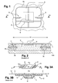
- a chip card type module 100 includes contact pads 9 within a zone of contact pads or peripheral P2.
- This dummy line device P2 designates the overall shape of the contact pads and does not include a concave part. This line corresponds substantially to the periphery of the receiving cavity (upper plane of the cavity) of the module.
- the module is embedded in a card body 1. It comprises legs J extending from a substantially central area of the contact pad to a connection area 3a, 3b through wells. Each leg J formed inside a contact pad 9 by a cut D of the latter.
- the cut J of the contact pad is oriented at 90 ° with respect to the main surface of the module.
- Holes corresponding to each cut D appear on the surface of the module and the smart card 100.
- the legs J penetrate into a conductive material filling the wells and in contact with the connection areas (without directly connecting the connection areas). The legs are fully engaged in the conductive material and do not directly connect the connection areas but through the conductive material.
- the invention relates to a method for connecting conductive pads 10 of a micromodule (2) to connection zones 3a, 3b embedded or accessible in a support 1 of a portable object 100.
- the portable object is a smart card 100 comprising a support body 1 (here a card body), an antenna 3, and a micromodule 2 embedded in a cavity 11 of the support body .
- the portable object may in particular be a multi-component card including a display and / or a keyboard and / or a sensor. It can be an electronic passport or an intelligent electronic key.
- the method comprises a step of supplying or producing a body of the portable object 1 comprising a cavity 11 for receiving the micromodule and connection zones 3a, 3b accessible in said cavity.
- the cavity opens out on the surface of the body and is delimited on the surface of the body by a first periphery,
- a body of the smart card is made with a cavity 11 here at two levels and connection pads 3a, 3b of a radiofrequency antenna 3 buried in the card body.
- the card is for example obtained by lamination of sheets or overmoulding of an electrical / electronic circuit, in particular supported by a sheet.
- the cavity defines a first periphery P1 or a periphery of the largest cavity opening on the surface of the body of the object.
- the cavity P1 and / or openings 5a, 5b allowing access to the connection areas 3a, 3b of the antenna circuit 3 can be achieved in particular by machining or during overmoulding by using a core occupying the cavity and / or openings.
- the card body comprises one or more holes (s) or recess (s) 5a, 5b which allow access to the connection areas 3a, 3b of the antenna 3 from outside the body.
- the antenna 3 is buried in the card body and comprises connection areas 3a, 3B accessible from outside the card body 1.
- the method also comprises a step of producing a micromodule 2 comprising electrical contact pads 10 on a front face delimited by a second periphery P2 substantially corresponding to or slightly smaller than the first periphery P1, connection portions bent towards a face back of the micromodule opposite to the front face.
- the micromodule 2 here comprises an integrated microcircuit 8.
- the micromodule here is substantially in accordance with the smart card micromodules. Here it comprises a coating E, chip connections 6 to the different contacts or contact pads.
- the module is here of simple type.
- the contact pads or conductors are formed on one side of the module including etching or against-bonding metallizations. The side for connecting a contact terminal is provided with these contact pads 10.
- 9 or conductive contact pads define a first peripheral P2 meaning to delimit the visible surface of contacts once the module inserted into a card body.
- Contact pads 9 include metal extensions (portions, tabs, connection tabs) extending from the pads 9. For example, to connect an antenna, two extensions are sufficient. For a more complex object such as a multi-component card, several extensions of ranges may be necessary.
- the micromodule here comprises contact pads 11 on the upper surface.
- the pads may be under a support substrate.
- portions of conductive pads are then folded before insertion into the cavity, towards the opposite face of that bearing the contact pads, in fact towards the support body 1.
- These portions 10 are here folded substantially at 90 ° to the face carrying the chip.
- the beach portions 10 may be supported by an insulating dielectric film.
- the folding can be carried out so that the conductive face of the portion is oriented substantially in a direction from the front face to the rear face of the module.
- connection portions that extend from the first periphery of the contact pads are configured so that in the folded position they can exert an elastic contact force against the connection areas after insertion into the cavity.
- At least one portion 10 is configured at a substantially right angle relative to the surface of the micromodule so as to bend slightly elastically at the insertion.
- the deformation may be elastic or plastic and elastic so as to maintain a certain holding force of the electrical contact.
- the method also comprises a step of insertion and connection of the module in the cavity, the connection portions being electrically connected with their respective connection zone (3a, 3b).
- the micromodule after having the folded portions is encased conventionally in the cavity 11 of the card body and fixed with, for example, a thermo-adhesive layer G, cyanoacrylate glue, etc. . as shown in the Figure 4B .
- connection portions extend from the first periphery of the contact pads; These portions may be configured to have elasticity in a direction substantially perpendicular to the main surface of the contact pads.
- the portions are preferably dimensioned with a greater length than the depth of the wells 5b, 5a so as to be slightly curved in particular by buckling during the insertion.
- An insertion tool can exert in this operation, a force on the entire surface of the module for elastic and / or plastic bonding and deformation of the connection portions (legs 10).
- the module conforms to that of the Figure 4A with the difference that the legs or connecting portions 10 have a much greater length than previously.
- At least one portion 10 is configured to form a zigzag or resilient spring and / or elastically deform at insertion.
- At least one portion Prior to insertion, at least one portion may be folded, configured to form an inward tilt of the module (toward the center of the module) and to deform at least elastically at insertion.
- the zigzag (or several folds on a connecting portion) can be formed before insertion including before or after the folding of the portions to the rear face of the module.
- the method may comprise a step of at least partial filling of each recess (5a, 5b) by a glue or conductive resin or not.
- the adhesive / resin serves to fix the portion in the elastic connection position against the connection areas. If necessary, contrary to FIG. 5D, only the bottom of the wells can be filled with glue / resin. Thus, a large intermediate portion of the connection portion 10 is free of movement between its end in contact with the connection area and its connection to the external surface contact area of the module at the peripheral line.
- the module here has several connection portions in particular for connecting one or more multi-component card circuit (s), in other embodiments, it may comprise only two portions of connections for example at the C4 ranges, C8 according to ISO 7816 to connect an antenna.
Landscapes
- Engineering & Computer Science (AREA)
- Computer Hardware Design (AREA)
- Microelectronics & Electronic Packaging (AREA)
- Physics & Mathematics (AREA)
- General Physics & Mathematics (AREA)
- Theoretical Computer Science (AREA)
- Credit Cards Or The Like (AREA)
- Combinations Of Printed Boards (AREA)
Priority Applications (3)
| Application Number | Priority Date | Filing Date | Title |
|---|---|---|---|
| EP13305150.8A EP2765536A1 (de) | 2013-02-07 | 2013-02-07 | Verfahren zur Verbindung eines Mikroschaltkreises mit leitenden Zonen, die in einem Träger zugänglich sind |
| EP14701070.6A EP2954462A1 (de) | 2013-02-07 | 2014-01-21 | Verfahren zum anschluss einer mikroschaltung an zugängliche leitfähige bereiche in einem träger |
| PCT/EP2014/051146 WO2014122009A1 (fr) | 2013-02-07 | 2014-01-21 | Procede de connexion d'un microcircuit a des zones conductrices accessibles dans un support |
Applications Claiming Priority (1)
| Application Number | Priority Date | Filing Date | Title |
|---|---|---|---|
| EP13305150.8A EP2765536A1 (de) | 2013-02-07 | 2013-02-07 | Verfahren zur Verbindung eines Mikroschaltkreises mit leitenden Zonen, die in einem Träger zugänglich sind |
Publications (1)
| Publication Number | Publication Date |
|---|---|
| EP2765536A1 true EP2765536A1 (de) | 2014-08-13 |
Family
ID=47843208
Family Applications (2)
| Application Number | Title | Priority Date | Filing Date |
|---|---|---|---|
| EP13305150.8A Withdrawn EP2765536A1 (de) | 2013-02-07 | 2013-02-07 | Verfahren zur Verbindung eines Mikroschaltkreises mit leitenden Zonen, die in einem Träger zugänglich sind |
| EP14701070.6A Withdrawn EP2954462A1 (de) | 2013-02-07 | 2014-01-21 | Verfahren zum anschluss einer mikroschaltung an zugängliche leitfähige bereiche in einem träger |
Family Applications After (1)
| Application Number | Title | Priority Date | Filing Date |
|---|---|---|---|
| EP14701070.6A Withdrawn EP2954462A1 (de) | 2013-02-07 | 2014-01-21 | Verfahren zum anschluss einer mikroschaltung an zugängliche leitfähige bereiche in einem träger |
Country Status (2)
| Country | Link |
|---|---|
| EP (2) | EP2765536A1 (de) |
| WO (1) | WO2014122009A1 (de) |
Cited By (1)
| Publication number | Priority date | Publication date | Assignee | Title |
|---|---|---|---|---|
| FR3030087A1 (fr) * | 2014-12-11 | 2016-06-17 | Oberthur Technologies | Module pour cartes a microcircuit, cartes a microcircuit comprenant un tel module et procede de fabrication |
Citations (6)
| Publication number | Priority date | Publication date | Assignee | Title |
|---|---|---|---|---|
| EP0225238A1 (de) * | 1985-11-08 | 1987-06-10 | Thomson Composants Militaires Et Spatiaux | Karten mit einem Bauelement und Mikromodul mit Seitenkontakten |
| US5598032A (en) | 1994-02-14 | 1997-01-28 | Gemplus Card International | Hybrid chip card capable of both contact and contact-free operation and having antenna contacts situated in a cavity for an electronic module |
| US5671525A (en) * | 1995-02-13 | 1997-09-30 | Gemplus Card International | Method of manufacturing a hybrid chip card |
| US5736781A (en) * | 1993-10-18 | 1998-04-07 | Oki Electric Industry Co., Ltd. | IC module and a data carrier employing the same |
| US5856912A (en) | 1997-03-04 | 1999-01-05 | Motorola Inc. | Microelectronic assembly for connection to an embedded electrical element, and method for forming same |
| EP2450837A1 (de) * | 2010-11-04 | 2012-05-09 | Gemalto SA | Verfahren zur Verbindung eines leitenden Bereichs mit einem elektrischen Kontakt durch eine Feder, und entsprechende Vorrichtung |
Family Cites Families (1)
| Publication number | Priority date | Publication date | Assignee | Title |
|---|---|---|---|---|
| FR2724477B1 (fr) * | 1994-09-13 | 1997-01-10 | Gemplus Card Int | Procede de fabrication de cartes sans contact |
-
2013
- 2013-02-07 EP EP13305150.8A patent/EP2765536A1/de not_active Withdrawn
-
2014
- 2014-01-21 EP EP14701070.6A patent/EP2954462A1/de not_active Withdrawn
- 2014-01-21 WO PCT/EP2014/051146 patent/WO2014122009A1/fr not_active Ceased
Patent Citations (6)
| Publication number | Priority date | Publication date | Assignee | Title |
|---|---|---|---|---|
| EP0225238A1 (de) * | 1985-11-08 | 1987-06-10 | Thomson Composants Militaires Et Spatiaux | Karten mit einem Bauelement und Mikromodul mit Seitenkontakten |
| US5736781A (en) * | 1993-10-18 | 1998-04-07 | Oki Electric Industry Co., Ltd. | IC module and a data carrier employing the same |
| US5598032A (en) | 1994-02-14 | 1997-01-28 | Gemplus Card International | Hybrid chip card capable of both contact and contact-free operation and having antenna contacts situated in a cavity for an electronic module |
| US5671525A (en) * | 1995-02-13 | 1997-09-30 | Gemplus Card International | Method of manufacturing a hybrid chip card |
| US5856912A (en) | 1997-03-04 | 1999-01-05 | Motorola Inc. | Microelectronic assembly for connection to an embedded electrical element, and method for forming same |
| EP2450837A1 (de) * | 2010-11-04 | 2012-05-09 | Gemalto SA | Verfahren zur Verbindung eines leitenden Bereichs mit einem elektrischen Kontakt durch eine Feder, und entsprechende Vorrichtung |
Cited By (1)
| Publication number | Priority date | Publication date | Assignee | Title |
|---|---|---|---|---|
| FR3030087A1 (fr) * | 2014-12-11 | 2016-06-17 | Oberthur Technologies | Module pour cartes a microcircuit, cartes a microcircuit comprenant un tel module et procede de fabrication |
Also Published As
| Publication number | Publication date |
|---|---|
| WO2014122009A1 (fr) | 2014-08-14 |
| EP2954462A1 (de) | 2015-12-16 |
Similar Documents
| Publication | Publication Date | Title |
|---|---|---|
| EP1062634B1 (de) | Chipkarte mit einer schleifenantenne und zugehöriges mikromodul | |
| EP2867831B1 (de) | Verfahren zur herstellung eines kontaktlosen mikrochips | |
| EP2877965B1 (de) | Elektronisches modul für eine chipkarte und gedruckte schaltung zur erzeugung eines solchen moduls | |
| EP0671705A2 (de) | Herstellungsverfahren einer kontaktlosen Karte und kontaktlose Karte | |
| EP3734493B1 (de) | Aufnahmeetui für chipkarte | |
| WO2006070140A1 (fr) | Module electronique double face pour carte a puce hybride | |
| EP2718877B1 (de) | Mikroschaltungsmodul und chipkarte ein solches enthaltend | |
| EP3408799B1 (de) | Verfahren zur herstellung eines chipkartenmoduls und chipkarte | |
| FR3088515A1 (fr) | Module electronique pour carte a puce | |
| EP2946343B1 (de) | Antennensystem für eine kontaktlose mikroschaltung | |
| EP3059698B1 (de) | Herstellungsverfahren eines einseitigen elektronischen Moduls, das Verbindungszonen umfasst | |
| FR2780534A1 (fr) | Procede de realisation d'objets portatifs a composants electroniques et objets portatifs tels qu'obtenus par ledit procede | |
| EP2765536A1 (de) | Verfahren zur Verbindung eines Mikroschaltkreises mit leitenden Zonen, die in einem Träger zugänglich sind | |
| EP1556832B1 (de) | Chipkarte mit einem auftauchenden bauelement und herstellungsverfahren | |
| EP2410472A1 (de) | Transponder-Einsatz und Vorrichtung, die einen solchen Einsatz umfasst | |
| WO2015132485A1 (fr) | Module électronique simplifié pour carte à puce à double interface de communication | |
| FR2786009A1 (fr) | Procede de fabrication d'une carte a puce hybride par impression double face | |
| FR2797075A1 (fr) | Procede de fabrication de dispositif portable a circuits integres, de type carte a puce de format reduit par rapport au format standard | |
| EP1724712A1 (de) | Micromodul, speziell für eine Smart Card | |
| WO2020114753A1 (fr) | Procede de fabrication d'une carte a puce metallique ou non avec antenne relais | |
| WO2020058036A1 (fr) | Procede de fabrication d'un module electronique pour objet portatif | |
| WO2017102110A1 (fr) | Procede de fabrication d'un dispositif comprenant un module electronique radiofrequence et un indicateur | |
| FR3084188A1 (fr) | Carte a puce equipee d'une pluralite d'antennes | |
| EP3166181A1 (de) | Herstellungsverfahren einer funkantenne auf einer halterung, und so erhaltene antenne | |
| FR3030087A1 (fr) | Module pour cartes a microcircuit, cartes a microcircuit comprenant un tel module et procede de fabrication |
Legal Events
| Date | Code | Title | Description |
|---|---|---|---|
| PUAI | Public reference made under article 153(3) epc to a published international application that has entered the european phase |
Free format text: ORIGINAL CODE: 0009012 |
|
| 17P | Request for examination filed |
Effective date: 20130207 |
|
| AK | Designated contracting states |
Kind code of ref document: A1 Designated state(s): AL AT BE BG CH CY CZ DE DK EE ES FI FR GB GR HR HU IE IS IT LI LT LU LV MC MK MT NL NO PL PT RO RS SE SI SK SM TR |
|
| AX | Request for extension of the european patent |
Extension state: BA ME |
|
| STAA | Information on the status of an ep patent application or granted ep patent |
Free format text: STATUS: THE APPLICATION IS DEEMED TO BE WITHDRAWN |
|
| 18D | Application deemed to be withdrawn |
Effective date: 20150214 |