EP2765596B1 - Implantation d'ions à des conditions d'équilibre de surface à haute température - Google Patents
Implantation d'ions à des conditions d'équilibre de surface à haute température Download PDFInfo
- Publication number
- EP2765596B1 EP2765596B1 EP14153892.6A EP14153892A EP2765596B1 EP 2765596 B1 EP2765596 B1 EP 2765596B1 EP 14153892 A EP14153892 A EP 14153892A EP 2765596 B1 EP2765596 B1 EP 2765596B1
- Authority
- EP
- European Patent Office
- Prior art keywords
- iii
- nitride semiconductor
- semiconductor body
- implantation
- chamber
- Prior art date
- Legal status (The legal status is an assumption and is not a legal conclusion. Google has not performed a legal analysis and makes no representation as to the accuracy of the status listed.)
- Active
Links
Images




Classifications
-
- H—ELECTRICITY
- H10—SEMICONDUCTOR DEVICES; ELECTRIC SOLID-STATE DEVICES NOT OTHERWISE PROVIDED FOR
- H10P—GENERIC PROCESSES OR APPARATUS FOR THE MANUFACTURE OR TREATMENT OF DEVICES COVERED BY CLASS H10
- H10P30/00—Ion implantation into wafers, substrates or parts of devices
- H10P30/20—Ion implantation into wafers, substrates or parts of devices into semiconductor materials, e.g. for doping
- H10P30/21—Ion implantation into wafers, substrates or parts of devices into semiconductor materials, e.g. for doping of electrically active species
-
- H—ELECTRICITY
- H01—ELECTRIC ELEMENTS
- H01J—ELECTRIC DISCHARGE TUBES OR DISCHARGE LAMPS
- H01J37/00—Discharge tubes with provision for introducing objects or material to be exposed to the discharge, e.g. for the purpose of examination or processing thereof
- H01J37/30—Electron-beam or ion-beam tubes for localised treatment of objects
- H01J37/317—Electron-beam or ion-beam tubes for localised treatment of objects for changing properties of the objects or for applying thin layers thereon, e.g. for ion implantation
- H01J37/3171—Electron-beam or ion-beam tubes for localised treatment of objects for changing properties of the objects or for applying thin layers thereon, e.g. for ion implantation for ion implantation
-
- H—ELECTRICITY
- H10—SEMICONDUCTOR DEVICES; ELECTRIC SOLID-STATE DEVICES NOT OTHERWISE PROVIDED FOR
- H10P—GENERIC PROCESSES OR APPARATUS FOR THE MANUFACTURE OR TREATMENT OF DEVICES COVERED BY CLASS H10
- H10P30/00—Ion implantation into wafers, substrates or parts of devices
- H10P30/20—Ion implantation into wafers, substrates or parts of devices into semiconductor materials, e.g. for doping
- H10P30/202—Ion implantation into wafers, substrates or parts of devices into semiconductor materials, e.g. for doping characterised by the semiconductor materials
- H10P30/206—Ion implantation into wafers, substrates or parts of devices into semiconductor materials, e.g. for doping characterised by the semiconductor materials into Group III-V semiconductors
-
- H—ELECTRICITY
- H01—ELECTRIC ELEMENTS
- H01J—ELECTRIC DISCHARGE TUBES OR DISCHARGE LAMPS
- H01J2237/00—Discharge tubes exposing object to beam, e.g. for analysis treatment, etching, imaging
- H01J2237/18—Vacuum control means
- H01J2237/188—Differential pressure
Definitions
- group III-V refers to a compound semiconductor including at least one group III element and at least one group V element.
- a group III-V semiconductor may take the form of a III-Nitride semiconductor.
- III-Nitride or “III-N” refers to a compound semiconductor that includes nitrogen and at least one group III element such as aluminum (Al), gallium (Ga), indium (In), and boron (B), and including but not limited to any of its alloys, such as aluminum gallium nitride (Al x Ga (1-x) N), indium gallium nitride (In y Ga (1-y) N), aluminum indium gallium nitride (Al x In y Ga (1-x-y) N), gallium arsenide phosphide nitride (GaAs a P b N (1-a-b) ), aluminum indium gallium arsenide phosphide nitride (A
- III-Nitride also refers generally to any polarity including but not limited to Ga-polar, N-polar, semi-polar, or non-polar crystal orientations.
- a III-Nitride material may also include either the Wurtzitic, Zincblende, or mixed polytypes, and may include single-crystal, monocrystalline, polycrystalline, or amorphous structures.
- Gallium nitride or GaN refers to a III-Nitride compound semiconductor wherein the group III element or elements include some or a substantial amount of gallium, but may also include other group III elements in addition to gallium.
- III-Nitride materials are semiconductor compounds that have relatively wide direct bandgaps and can have strong piezoelectric polarizations, which can enable high breakdown fields, high saturation velocities, and the creation of two-dimensional electron gases (2DEGs), when combined as stacked layers.
- 2DEGs two-dimensional electron gases
- III-Nitride materials are suitable for use in many microelectronic applications as field-effect transistors (FETs), including heterostructure FETs (HFETs) such as high electron mobility transistors (HEMTs).
- FETs field-effect transistors
- HFETs heterostructure FETs
- HEMTs high electron mobility transistors
- III-Nitride semiconductor device fabrication is doping a III-Nitride semiconductor body without compromising its stoichiometric integrity.
- nitrogen may escape from the III-Nitride surface, resulting in its decomposition.
- a conventional approach to address this problem utilizes a technique for growing the dopants into the III-Nitride body as it is formed, rather than performing ion implantation.
- a significant drawback of that approach is that it results in formation of relatively homogenously doped layers within the III-Nitride body. Consequently, differential doping is typically achieved only vertically, so that spatially confined doping in the lateral direction may not be achieved directly through such growth except through the use of relatively complex and expensive etch and redeposition/regrowth methods.
- WO 2010/051266 A1 describes a method comprising situating a semiconductor body in a surface equilibrium chamber establishing a gas pressure heating said III-Nitride semiconductor body to an elevated implantation temperature in said surface equilibrium chamber while substantially maintaining said gas pressure, "temperature may be maintained at between about 10 degrees Celsius and about 500 degrees Celsius"; implanting said III-Nitride semiconductor body in said surface equilibrium chamber at said elevated implantation temperature while substantially maintaining said gas pressure.
- WO 2009/029329 A discloses a high temperature (e.g. 650°C) ion beam implantation process for a III-Nitride semiconductor body.
- a method comprises situating a III-Nitride semiconductor body in a surface equilibrium chamber configured to prevent an escape of nitrogen from said III-Nitride semiconductor body during implantation of said III-Nitride semiconductor body, establishing a gas pressure greater than or equal to a surface equilibrium pressure sufficient to prevent said escape of nitrogen from said III-Nitride semiconductor body, heating said III-Nitride semiconductor body to an implantation temperature in a range of 500°C to 1100°C in said surface equilibrium chamber while substantially maintaining said gas pressure above an exposed surface of said III-Nitride semiconductor body, implanting said III-Nitride semiconductor body in said surface equilibrium chamber at said elevated implantation temperature while substantially maintaining said gas pressure in a range between 1.0 and 1000 mTorr, wherein said implanting is performed using an ion implanter interfacing with said surface equilibrium chamber.
- the present application is directed to a method and system for ion implantation of a III-Nitride semiconductor body.
- ion implantation of the III-Nitride semiconductor body may be performed at elevated temperatures and equilibrium pressure in an implantation chamber.
- ion implantation may be performed in the surface and near surface regions of the III-Nitride semiconductor body.
- the present solution can eliminate or reduce the requirements for post implant high temperature anneals, required for dopant activation, that are typically a necessity in the conventional art.
- the present solution may provide a system enabling dopant activation through in-situ annealing of the implant damage and activation of the dopants, while avoiding the decomposition of the III-Nitride semiconductor body stoichiometry.
- Figure 1 shows a cross-sectional diagram of implantation chamber 100 for ion implantation at high temperature surface equilibrium conditions, according to one implementation.
- implantation chamber 100 includes surface equilibrium chamber 110, ion implanter 130, and transition chamber 120 interfacing ion implanter 130 with surface equilibrium chamber 110.
- transition chamber 120 includes differential pressure cells 122a, 122b, and 122c.
- III-Nitride semiconductor body 140 such as a gallium nitride (GaN) body, for example, grown over support substrate 112.
- Support substrate 112 may be any suitable substrate material for the growth of III-Nitride semiconductor body, and may include silicon, silicon carbide, sapphire, and when available, a native III-Nitride semiconductor substrate, for example.
- surface equilibrium chamber 110 includes platform 106, which may be a rotating platform or a controllably moveable platform, for example, on which support substrate 112 and III-Nitride semiconductor body 140 may be placed during ion implantation of III-Nitride semiconductor body 140.
- platform 106 which may be a rotating platform or a controllably moveable platform, for example, on which support substrate 112 and III-Nitride semiconductor body 140 may be placed during ion implantation of III-Nitride semiconductor body 140.
- surface equilibrium chamber 110 is equipped with intake port 102 to allow for the entry of a gas or gases for establishing surface equilibrium conditions for III-Nitride semiconductor body 140, as well as output port 104 for the removal of such gas or gases.
- Surface equilibrium chamber 110 is designed such that the equilibrium pressure within surface equilibrium chamber 110 is controlled to sustain a partial vacuum range of approximately one to approximately one thousand millitorr (1.0 - 1000 mTorr). 1 mTorr is about 0.1333 Pa. In one implementation, for example, surface equilibrium
- Ion implanter 130 may provide ions for implantation into III-Nitride semiconductor body 140 as ion beam 132, and may perform selective implantation of portions of III-Nitride semiconductor body 140.
- ion implanter 130 is an apparatus that produces and may focus ion beam 132 of substantially identical ions having a well controlled velocity and mass from a solid or gaseous source material.
- ion beam 132 can be a focused ion beam with the ability to write or raster over the surface of III-Nitride semiconductor body 140, such as by being steered over the surface of III-Nitride semiconductor body 140.
- ion beam 132 can be a wide area focused ion beam allowing for blanket ion implantation, or implantation using stencil masks or sacrificial mask layers over a larger area of III-Nitride semiconductor body 140.
- Such masks may include common materials well known in the art, and may be organically based, or may be formed of photo-resist, silicon dioxide, or silicon nitride, for example.
- Transition chamber 120 may be utilized to provide a suitable environment, such as a low pressure or high vacuum environment, for ion implanter 130 and its interaction with surface equilibrium chamber 110. Transition chamber 120 serves to interface ion implanter 130 with surface equilibrium chamber 110, which is configured to provide surface equilibrium conditions for III-Nitride semiconductor body 140 during ion implantation.
- transition chamber 120 may include several differential pressure cells 122a, 122b, and 122c. Each differential pressure cell 122a, 122b, and 122c is in communication with an adjacent differential pressure cell through respective apertures 126ab and 126bc. It is noted that ion beam 132 passes through apertures 126bc and 126ab to travel through transition chamber 120, which interfaces ion implanter 130 with surface equilibrium chamber 110 through linking aperture 128. Differential pressure cells 122a, 122b, and 122c may be selectably evacuated using respective pumping apertures 124a, 124b, and 124c.
- differential pressure cell 122c of transition chamber 120 may also include Faraday cup 114.
- Faraday cup 114 may be linked to a current meter (not shown in Figure 1 ) to measure the implant dosage of ions being received from ion implanter 130.
- Faraday cup 114 may be attached to bellows 118 (or another type of mechanical linear actuator used in vacuum technology) to allow Faraday cup 114 to be moved into and out of the path of ion beam 132.
- bellows 118 or another type of mechanical linear actuator used in vacuum technology
- Such ion neutralization may occur as ion beam 132 passes through differential pressure cells 122a, 122b, and 122c, and surface equilibrium chamber 110.
- Faraday cup 114 may be incorporated into aperture 126bc.
- Faraday cup 114 may be periodically positioned in the path of ion beam 132 (e.g., approximately 1% of the time) in order to measure the implant dosage being directed at III-Nitride semiconductor body 140, thereby enabling estimation of the concentration of ions implanted into III-Nitride semiconductor body 140. This periodic positioning may be accomplished by actuation of bellows 118 at a predetermined periodicity.
- Faraday cup 114 may be mounted on a rotating plate or wheel or armature (not shown in Figure 1 ) within differential pressure cell 122c, such that Faraday cup 114 rotates under ion beam 132 at a predetermined rate (e.g., 1% of the implant time).
- Transistion chamber 120 may further include deflection plates, such as deflection plates 116, positioned inside differential pressure cell 122b, for example, near aperture 126bc.
- deflection plates 116 may be used to change the direction of ion beam 132 entering surface equilibrium chamber 110, for example, so as to steer ion beam 132 over the surface of III-Nitride semiconductor body 140.
- FIG. 2 shows a cross-sectional view of implantation chamber 200 for performing ion implantation at high temperature surface equilibrium conditions, according to another implementation.
- Implantation chamber 200 includes surface equilibrium chamber 210, ion implanter 230, and transition chamber 220 interfacing ion implanter 230 with surface equilibrium chamber 210.
- Transition chamber 220 includes differential pressure cells 222a, 222b, and 222c having respective differential pumping apertures 224a, 224b, and 224c.
- Surface equilibrim chamber 210 includes intake port 202, output port 204, and platform 206.
- III-Nitride semiconductor body 240 and support substrate 212 are situated on platform 206.
- Implantation chamber 200 including surface equilibrium chamber 210, ion implanter 230, and transition chamber 220 corresponds in general to implantation chamber 100 including surface equilibrium chamber 110, ion implanter 130, and transition chamber 120, in Figure 1 .
- ion beam 232 may be a focused ion beam produced so as to impinge upon III-Nitride semiconductor body 240 in the absence of ion beam steering, provided, for example, by deflection plates 116, in Figure 1 .
- platform 206 is shown as a controllably moveable platform, such as a rotating platform for example, as indicated by linear displacement lines 207a and/or rotational arrows 207b.
- aperture 226ab and linking aperture 228 may be made much smaller, and the pressure in transition chamber 220 can more easily reduced, than in the implementation shown in Figure 1 .
- exemplary implantation chambers 100 and 200 will be further described by reference to flowchart 300, in Figure 3 , which outlines an exemplary method for performing ion implantation of a III-Nitride semiconductor body at high temperature surface equilibrium conditions. It is noted that certain details and features have been left out of flowchart 300 that are apparent to a person of ordinary skill in the art.
- III-Nitride semiconductor body 140/240 may be grown over support substrate 112/212, which may be any suitable substrate for III-Nitride growth, such as a silicon, silicon carbide (SiC), or aluminum oxide (Al 2 O 3 ) substrate, or a native III-Nitride substrate, for example.
- support substrate 112/212 may be any suitable substrate for III-Nitride growth, such as a silicon, silicon carbide (SiC), or aluminum oxide (Al 2 O 3 ) substrate, or a native III-Nitride substrate, for example.
- silicon substrate refers to a semiconductor substrate that includes at least one layer of silicon.
- silicon based composite substrates such as silicon-on-insulator (SOI) and separation by implantation of oxygen (SIMOX) process substrates, as well as silicon on sapphire (SOS) substrates for example.
- SOI silicon-on-insulator
- SIMOX separation by implantation of oxygen
- SOS silicon on sapphire
- Such a silicon substrate may also contain silicon devices and vias formed on or within the silicon substrate.
- III-Nitride semiconductor body 140/240 may occur in implantation chamber 100/200.
- surface equilibrium chamber 110/210 may have been configured as a growth chamber 110/210 during a growth phase of III-Nitride semiconductor body 140/240. That is to say, chamber 110/210 may be configurable first as growth chamber 110/210 and subsequently as surface equilibrium chamber 110/210 during fabrication and processing of III-Nitride semiconductor body 140/240. In other implementations, however, III-Nitride semiconductor body 140/240 may be grown in a growth chamber apart from ion implantation chamber 100/200.
- III-Nitride semiconductor body 140/240 may be performed using any suitable growth technique, such as metalorganic chemical vapor deposition (MOCVD) or molecular-beam epitaxy (MBE), for example. Growth of III-Nitride semiconductor body 140/240 may occur in any suitable atmospheric and thermal environment for growing III-Nitride materials, such as in the presence of nitrogen gas or a nitrogen precursor gas like ammonia, as well as additional reactant gases such as trimethylgallium (TMG) and trimethylaluminum (TMA), for instance.
- MOCVD metalorganic chemical vapor deposition
- MBE molecular-beam epitaxy
- III-Nitride semiconductor body 140/240 may be grown using the MOCVD technique and may be deposited on support substrate 112/212, which may be a silicon substrate.
- III-Nitride semiconductor body 140/240 may include an amorphous silicon aluminum nitride based layer, one or more aluminum nitride (AlN) nucleation layers, compositionally graded transition layers, one or more strain absorbing transition interlayer modules, a buffer layer, a channel layer, an AlN spacer layer, one or more barrier layers, and/or one or more III-Nitride capping layers.
- AlN aluminum nitride
- Flowchart 300 continues with determining an implantation temperature for ion implantation of III-Nitride semiconductor body 140/240 (310). More generally, however, such a determination may include identifying additional implantation conditions for ion implantation of III-Nitride semiconductor body 140/240. In addition to determination of implantation temperature, implantation conditions to be identified may include a number of other variables, such as the ion species to be implanted, the desired depth of implantation, and the gas species used in the surface equilibration chamber 110/210 to be utilized during implantation, for example.
- implantation conditions may include whether ion beam 132/232 is to be a focused ion beam with the ability to write or raster over the surface of III-Nitride semiconductor body 140/240, or whether ion beam 132/232 is to be a wide area defocused ion beam allowing for a blanket, stenciled, or sacrificially masked, ion implantation over a larger area of III-Nitride semiconductor body 140/240.
- III-Nitride semiconductor body 140/240 in implantation chamber 100/200 (320). As shown in Figures 1 and 2 , III-Nitride semiconductor body 140/240 and support substrate 112/212 may be situated in surface equilibrium chamber 110/210 of implantation chamber 100/200. As noted above, III-Nitride semiconductor body 140/240 may have been grown over support substrate 112/212 prior to its being situated in surface equilibrium chamber 110/210 of implantation chamber 100/200.
- III-Nitride semiconductor body 140/240 may correspond to a body formed from any one or more suitable III-Nitride semiconductor materials, as are described in the definition section above. Typically, the only constraint placed upon the composition of III-Nitride semiconductor body 140/240 is that it include at least one layer of III-Nitride semiconductor material.
- III-Nitride semiconductor body 140/240 may include a first III-Nitride semiconductor layer and a second III-Nitride semiconductor layer formed over the first III-Nitride semiconductor layer, for example, wherein the second III-Nitride semiconductor layer includes a III-Nitride semiconductor having a wider band gap than the III-Nitride semiconductor forming the first III-Nitride semiconductor layer.
- III-Nitride semiconductor body 140/240 may include a heterojunction formed by the interface of a GaN channel layer and an aluminum gallium nitride (AlGaN) barrier layer formed over the GaN channel layer.
- AlGaN aluminum gallium nitride
- Other examples of III-Nitride semiconductor bodies corresponding to III-Nitride semiconductor body 140/240 include commonly used epilayers found within the structures of microelectronic and optoelectronic III-Nitride devices including transistors, diodes, light-emitting diodes (LEDs), laser diodes, detectors, and sensors.
- Flowchart 300 continues with establishing a gas pressure (i.e., gas overpressure) greater than or approximately equal to a surface equilibrium pressure of III-Nitride semiconductor body 140/240 (330).
- the gas pressure may be established within implantation chamber 100/200, using surface equilibrium chamber 110/210, based on the previously identified implantation conditions and the material composition of III-Nitride semiconductor body 140/240, typically within the partial vacuum range of about 1.0 - 1000 mTorr.
- Establishing the desired gas pressure may be accomplished by controlling the gas pressure within surface equilibrium chamber 110/210 through use of intake port 102/202 and output port 104/204.
- the source gas or gases for establishing the gas pressure at a surface of III-Nitride semiconductor body 140/240 may be selected from any suitable nitrogen containing gas, such as nitrogen gas or ammonia, for example.
- the specific gas pressure required to prevent decomposition of III-Nitride semiconductor body 140/240 is dependent on factors such as the composition of the surface layer of III-Nitride semiconductor body 140/240, the temperature of III-Nitride semiconductor body 140/240, and the specific gas species being utilized. As a result, the gas pressure required will change with the temperature of III-Nitride semiconductor body 140/240, and the apparatus will be required to adjust the pressure so as to maintain the equilibrium condition and prevent decomposition of at a surface of III-Nitride semiconductor body 140/240.
- III-Nitride semiconductor body 140/240 may be heated to an elevated implantation temperature while the gas pressure within surface equilibrium chamber 110/210 is controlled such that a surface layer of III-Nitride semiconductor body 140/240 does not decompose.
- III-Nitride semiconductor body 140/240 may be heated to an elevated implantation temperature in a range from approximately five hundred degrees Centigrad (500 °C) to approximately eleven hundred degrees Centigrade (1100 °C).
- III-Nitride semiconductor body 140/240 is described as being situated in implantation chamber 100/200 before establishment of the implantation temperature, including heating of platform 106/206, that is only one possibility.
- the implantation temperature may be established and platform 106/206 of implantation chamber 100/200 may be preheated to or near the implantation temperature before III-Nitride semiconductor body 140/240 is situated therein.
- Flowchart 300 continues with implanting III-Nitride semiconductor body 140/240 in implantation chamber 100/200 while substantially maintaining the gas pressure above the exposed surface of III-Nitride semiconductor body 140/240 at greater than or approximately equal to the surface equilibrium pressure of III-Nitride semiconductor body 140/240 (350). Substantially maintaining the gas pressure at greater than or approximately equal to the surface equilibrium pressure of III-Nitride semiconductor body 140/240 may be performed using surface equilibrium chamber 110/210 of implantation chamber 100/200.
- Implantation may be performed using ion implanter 130/230 interfacing with surface equilibrium chamber 110/210, and may result in any desired ion species being implanted into III-Nitride semiconductor body 140/240.
- N type dopant ion such as silicon (Si) ions
- P type dopant ions such as magnesium (Mg) ions, for example, may be implanted into III-Nitride semiconductor body 140/240.
- the implantation conditions may include use of one or more stencils to form corresponding one or more spatially confined implantation regions at or beneath the surface of III-Nitride semiconductor body 140/240.
- implantation may include steering of ion beam 132/232, or movement of III-Nitride semiconductor body 140/240, during implantation so as to produce one or more spatially confined implantation regions at or beneath the surface of III-Nitride semiconductor body 140/240.
- movement of III-Nitride semiconductor body 140/240 during implantation may be achieved through controlled movement of platform 106/206.
- N type doping and P type doping may both be performed, resulting in formation of a spatially confined N type region laterally adjacent a spatially confined P type region in III-Nitride semiconductor body 140/240.
- relatively low energy surface implantation of III-Nitride semiconductor body 140/240 may be advantageous or desirable, utilizing implantation energies of less than approximately 100 keV, for example. That is to say, in some implementations, relatively low implantation energies may be used in order to implant dopant ions near the surface of III-Nitride semiconductor body 140/240. In other implementations, however, deeper penetration into III-Nitride semiconductor body 140/240 may be desired, so that higher implantation energies may be employed.
- III-Nitride semiconductor body 140/240 can be doped to any reasonably achievable concentration, for example, to a concentration from approximately 10 11 /cm 2 to approximately 10 19 /cm 2 .
- Flowchart 300 continues with optionally performing a substantial anneal of III-Nitride semiconductor body 140/240 to anneal ion implantation damage and substantially activate the implanted dopant(s) (360).
- the temperature of implanted III-Nitride semiconductor body 140/240 may be adjusted to an appropriate annealing temperature to substantially anneal any damage that may have occurred to the III-Nitride crystal structure from the impinging high energy ions, as well as to substantially electrically activate the implanted dopants. That is to say, the method of flowchart 300 may include annealing III-Nitride semiconductor body 140/240 in-situ at elevated temperature post implantation to achieve substantial dopant activation.
- Flowchart 300 may conclude with cooling down the III-Nitride body, for example to approximately room temperature, while maintaining the surface equilibrium pressure (370). Once the III-Nitride body is cooled to the desired temperature, the III-Nitride body may be removed from the implant chamber.
- the gas pressure within surface equilibrium chamber 110/210 is substantially maintained during implantation of III-Nitride semiconductor body 140/240.
- Substantially maintaining the gas pressure during implantation substantially prevents decomposition of III-Nitride semiconductor body 140/240 during implantation, despite its being exposed to an elevated implantation temperature. Consequently, the structural and stoichiometric properties of III-Nitride semiconductor body 140/240 can by preserved during implantation.
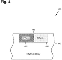
- Figure 4 shows a cross-sectional representation of a P-N junction formed in a III-Nitride semiconductor body as a result of ion implantation at high temperature surface equilibrium conditions, according to one implementation.
- Structure 400 in Figure 4 , includes P type region 442 and N type region 444 formed in III-Nitride semiconductor body 440.
- III-Nitride semiconductor body 440 corresponds in general to III-Nitride semiconductor body 140/240, shown in Figure 1 / 2 , and may share any of the characteristics attributed to that corresponding feature, above.
- both P type region 442 and N type region 444 are spatially confined within III-Nitride semiconductor body 440, and have been selectively formed so as to be laterally adjacent one another. Moreover, spatially confined P type region 442 and spatially confined N type region 444 have been advantageously implanted to be laterally spatially confined and adjoining within III-Nitride body 440 so as to produce P-N junction 446 at their interface/overlap. Structure 400 may be utilized in the implementation of a diode, for example, or a portion of a bipolar junction transistor fabricated in III-Nitride body 440.
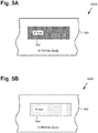
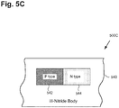
- Figures 5A, 5B , and 5C show respective cross-sectional representations of buried P type and/or N type regions formed in a III-Nitride semiconductor body as a result of ion implantation at high temperature surface equilibrium conditions, according to various implementations.
- Structure 500A, in Figure 5A includes spatially confined P type region 542 formed in III-Nitride semiconductor body 540.
- III-Nitride semiconductor body 540 corresponds in general to III-Nitride semiconductor body 140/240, shown in Figure 1 / 2 , and may share any of the characteristics attributed to that corresponding feature, above.
- P type region 542 is spatially confined within III-Nitride semiconductor body 540 and is buried to a predetermined depth beneath a top surface of III-Nitride semiconductor body 540.
- structure 500B includes spatially confined N type region 544 formed in III-Nitride semiconductor body 540.
- N type region 544 is spatially confined within III-Nitride semiconductor body 540 and is buried to a predetermined depth beneath the top surface of III-Nitride semiconductor body 540.
- structure 500C includes spatially confined P type region 542 and spatially confined N type region 544 formed in III-Nitride semiconductor body 540.
- P type region 542 and N type region 544 are spatially confined within III-Nitride semiconductor body 540, and can be selectively formed so as to be laterally adjacent or adjoining one another.
- P type region 542 and N type region 544 are spatially confined within III-Nitride semiconductor body 540 and are buried to a predetermined depth beneath the top surface of III-Nitride semiconductor body 540.
- Figures 6A, 6B , and 6C show respective cross-sectional representations of vertically stacked P type and N type regions formed in a III-Nitride semiconductor body as a result of ion implantation at high temperature surface equilibrium conditions, according to various implementation.
- Structure 600A, in Figure 6A includes spatially confined N type region 644 formed in III-Nitride semiconductor body 640, and spatially confined P type region 642 formed at or near a top surface of III-Nitride semiconductor body 640 and stacked over N type region 644.
- III-Nitride semiconductor body 640 corresponds in general to III-Nitride semiconductor body 140/240, shown in Figure 1 / 2 , and may share any of the characteristics attributed to that corresponding feature, above.
- structure 600B includes spatially confined N type region 644 formed in III-Nitride semiconductor body 640 and stacked over spatially confined P type region 642. As shown in Figure 5B , P type region 642 and N type region 644 are spatially confined within III-Nitride semiconductor body 640 and are buried to respective predetermined depths beneath the top surface of III-Nitride semiconductor body 640.
- FIGS. 6A and 6B depict formation of two different implanted regions spatially confined within III-Nitride semiconductor body 640 and stacked vertically on one another, it is noted that more than two spatially confined implanted regions may be formed, for example P-N-P and N-P-N vertically stacked arrangements.
- Figure 6C shows an example of a P-N-P structure.
- P type regions 642a and 642b, and N type region 644 are spatially confined within III-Nitride semiconductor body 640, and have been selectively formed so that N type region 644 is formed between P type region 642a and P type region 642b within III-Nitride semiconductor body 640.
- the upper doped region (e.g., P type region 642a, in Figure 6C ) may be formed at or near the top surface of III-Nitride semiconductor body 640, or may be buried so as to be situated at a substantial depth beneath the the top surface of III-Nitride semiconductor body 640.
- the lower doped region (e.g., P type region 642b, in Figure 6C ) may be formed at or near a bottom surface of III-Nitride semiconductor body 640, or may be situated at a height substantially above the bottom surface.
- the concepts disclosed by the present application enable laterally selective, spatially confined ion implantation of a III-Nitride semiconductor body at an elevated implantation temperature, while concurrently preserving the structural and stoichiometric properties of the semiconductor material.
- the present application discloses an approach that makes it possible to advantageously perform junction engineering in a III-Nitride semiconductor body.
- the present inventive concepts may be applied to facilitate either N type or P type dopant implantation, the fabrication of bipolar or reduced surface field (RESURF) devices is rendered significantly easier to achieve.
- RESURF reduced surface field
Landscapes
- Chemical & Material Sciences (AREA)
- Analytical Chemistry (AREA)
- Recrystallisation Techniques (AREA)
- Crystals, And After-Treatments Of Crystals (AREA)
Claims (5)
- Procédé comprenant :situer un corps semi-conducteur en nitrure III dans une chambre d'équilibre de surface configurée pour empêcher un dégagement d'azote du corps semi-conducteur de nitrure III pendant une implantation du corps semi-conducteur de nitrure III;établir une pression gazeuse supérieure ou égale à une pression d'équilibre de surface suffisante pour empêcher le dégagement d'azote du corps semi-conducteur de nitrure III;porter le corps de semi-conducteur de nitrure III à une température d'implantation dans une plage de 500°C à 1100°C dans la chambre d'équilibre de surface, tout en maintenant sensiblement la pression gazeuse au dessus d'une surface mise à nu du corps semi-conducteur de nitrure III;le procédé comprenant les caractéristiques suivantes :implanter le corps semi-conducteur de nitrure III dans la chambre d'équilibre de surface à la température d'implantation élevée, tout en maintenant la pression gazeuse dans une plage comprise entre 1,0 et 1000 mTorr;dans lequel on effectue l'implantation en utilisant un implanteur d'ions en interface avec la chambre d'équilibre de surface.
- Procédé suivant la revendication 1, dans lequel l'implantation se traduit par la formation d'une région dopée confinée spatialement latéralement dans le corps semi-conducteur de nitrure III.
- Procédé suivant la revendication 1, dans lequel on active électriquement des agents de dopage implantés dans le corps semi-conducteur de nitrure III sans dégagement d'azote d'une surface du corps semi-conducteur de nitrure III.
- Procédé suivant la revendication 1, dans lequel l'implantation se traduit par la formation d'au moins une région de type N confinée spatialement et une région de type P confinée spatialement dans le corps semi-conducteur de nitrure III.
- Procédé suivant la revendication 1, dans lequel l'implantation se traduit par la formation d'une jonction P-N dans le corps semi-conducteur de nitrure III.
Applications Claiming Priority (3)
| Application Number | Priority Date | Filing Date | Title |
|---|---|---|---|
| US201361763895P | 2013-02-12 | 2013-02-12 | |
| US13/788,318 US8692219B2 (en) | 2007-06-25 | 2013-03-07 | Method and apparatus for growing a III-nitride layer |
| US14/170,293 US9218991B2 (en) | 2007-06-25 | 2014-01-31 | Ion implantation at high temperature surface equilibrium conditions |
Publications (2)
| Publication Number | Publication Date |
|---|---|
| EP2765596A1 EP2765596A1 (fr) | 2014-08-13 |
| EP2765596B1 true EP2765596B1 (fr) | 2018-07-11 |
Family
ID=50030213
Family Applications (1)
| Application Number | Title | Priority Date | Filing Date |
|---|---|---|---|
| EP14153892.6A Active EP2765596B1 (fr) | 2013-02-12 | 2014-02-04 | Implantation d'ions à des conditions d'équilibre de surface à haute température |
Country Status (2)
| Country | Link |
|---|---|
| EP (1) | EP2765596B1 (fr) |
| JP (1) | JP6092794B2 (fr) |
Citations (1)
| Publication number | Priority date | Publication date | Assignee | Title |
|---|---|---|---|---|
| WO2009029329A1 (fr) * | 2007-08-29 | 2009-03-05 | Cree, Inc. | Implantation d'ions à haute température de transistors à électrons à grande mobilité à base de nitrure |
Family Cites Families (8)
| Publication number | Priority date | Publication date | Assignee | Title |
|---|---|---|---|---|
| FR2747840B1 (fr) * | 1996-04-22 | 1998-09-11 | Motorola Semiconducteurs | Appareil d'irradiation combinee par un faisceau d'ions et un rayonnement micro-onde, et procede associe |
| US7137354B2 (en) * | 2000-08-11 | 2006-11-21 | Applied Materials, Inc. | Plasma immersion ion implantation apparatus including a plasma source having low dissociation and low minimum plasma voltage |
| US7341628B2 (en) * | 2003-12-19 | 2008-03-11 | Melas Andreas A | Method to reduce crystal defects particularly in group III-nitride layers and substrates |
| JP2006156441A (ja) * | 2004-11-25 | 2006-06-15 | Nikon Corp | イオン注入装置、及びイオン注入方法 |
| US8395132B2 (en) * | 2007-06-25 | 2013-03-12 | International Rectifier Corporation | Ion implanting while growing a III-nitride layer |
| US8093597B2 (en) * | 2007-06-25 | 2012-01-10 | International Rectifier Corporation | In situ dopant implantation and growth of a III-nitride semiconductor body |
| CN102203912B (zh) * | 2008-10-31 | 2013-11-13 | 应用材料公司 | 改善p3i腔室中共形掺杂的方法 |
| US8518808B2 (en) * | 2010-09-17 | 2013-08-27 | The United States Of America, As Represented By The Secretary Of The Navy | Defects annealing and impurities activation in III-nitride compound |
-
2014
- 2014-02-04 EP EP14153892.6A patent/EP2765596B1/fr active Active
- 2014-02-05 JP JP2014020469A patent/JP6092794B2/ja active Active
Patent Citations (1)
| Publication number | Priority date | Publication date | Assignee | Title |
|---|---|---|---|---|
| WO2009029329A1 (fr) * | 2007-08-29 | 2009-03-05 | Cree, Inc. | Implantation d'ions à haute température de transistors à électrons à grande mobilité à base de nitrure |
Also Published As
| Publication number | Publication date |
|---|---|
| JP6092794B2 (ja) | 2017-03-08 |
| EP2765596A1 (fr) | 2014-08-13 |
| JP2014179589A (ja) | 2014-09-25 |
Similar Documents
| Publication | Publication Date | Title |
|---|---|---|
| TWI707975B (zh) | 半導體元件用磊晶基板、半導體元件以及半導體元件用磊晶基板之製造方法 | |
| US8093597B2 (en) | In situ dopant implantation and growth of a III-nitride semiconductor body | |
| JP6052420B2 (ja) | 半導体装置の製造方法 | |
| US11444172B2 (en) | Method for producing semiconductor device and semiconductor device | |
| WO2017077989A1 (fr) | Substrat épitaxial pour éléments semi-conducteurs, élément semi-conducteur et procédé de fabrication de substrats épitaxiaux pour éléments semi-conducteurs | |
| CN108352327B (zh) | 半导体元件用外延基板、半导体元件和半导体元件用外延基板的制造方法 | |
| US9218991B2 (en) | Ion implantation at high temperature surface equilibrium conditions | |
| EP2765596B1 (fr) | Implantation d'ions à des conditions d'équilibre de surface à haute température | |
| EP3863064A1 (fr) | Transistor à haute mobilité électronique et son procédé de fabrication | |
| US20240153766A1 (en) | Method of manufacturing nitrogen-face nitride semiconductor and nitrogen-face nitride semiconductor device manufactured using the same | |
| JP6416705B2 (ja) | 電界効果トランジスタおよびその製造方法 | |
| JP6582736B2 (ja) | 窒化物半導体装置の製造方法 | |
| JP3349316B2 (ja) | エピタキシャル成長方法 | |
| JP2017208438A (ja) | 窒化物半導体装置および窒化物半導体装置の製造方法 | |
| KR20250151142A (ko) | AlN 후막 기반의 GaN HEMT 에피택시 웨이퍼 및 그 제조 방법 | |
| JP2003318444A (ja) | Iii族窒化物系化合物半導体素子の製造方法 | |
| GB2425653A (en) | Manufacture of group III-nitride semiconductor |
Legal Events
| Date | Code | Title | Description |
|---|---|---|---|
| PUAI | Public reference made under article 153(3) epc to a published international application that has entered the european phase |
Free format text: ORIGINAL CODE: 0009012 |
|
| 17P | Request for examination filed |
Effective date: 20140204 |
|
| AK | Designated contracting states |
Kind code of ref document: A1 Designated state(s): AL AT BE BG CH CY CZ DE DK EE ES FI FR GB GR HR HU IE IS IT LI LT LU LV MC MK MT NL NO PL PT RO RS SE SI SK SM TR |
|
| AX | Request for extension of the european patent |
Extension state: BA ME |
|
| R17P | Request for examination filed (corrected) |
Effective date: 20150206 |
|
| RBV | Designated contracting states (corrected) |
Designated state(s): AL AT BE BG CH CY CZ DE DK EE ES FI FR GB GR HR HU IE IS IT LI LT LU LV MC MK MT NL NO PL PT RO RS SE SI SK SM TR |
|
| 17Q | First examination report despatched |
Effective date: 20150602 |
|
| GRAP | Despatch of communication of intention to grant a patent |
Free format text: ORIGINAL CODE: EPIDOSNIGR1 |
|
| STAA | Information on the status of an ep patent application or granted ep patent |
Free format text: STATUS: GRANT OF PATENT IS INTENDED |
|
| RAP1 | Party data changed (applicant data changed or rights of an application transferred) |
Owner name: INFINEON TECHNOLOGIES AMERICAS CORP. |
|
| INTG | Intention to grant announced |
Effective date: 20180209 |
|
| GRAS | Grant fee paid |
Free format text: ORIGINAL CODE: EPIDOSNIGR3 |
|
| GRAA | (expected) grant |
Free format text: ORIGINAL CODE: 0009210 |
|
| STAA | Information on the status of an ep patent application or granted ep patent |
Free format text: STATUS: THE PATENT HAS BEEN GRANTED |
|
| AK | Designated contracting states |
Kind code of ref document: B1 Designated state(s): AL AT BE BG CH CY CZ DE DK EE ES FI FR GB GR HR HU IE IS IT LI LT LU LV MC MK MT NL NO PL PT RO RS SE SI SK SM TR |
|
| REG | Reference to a national code |
Ref country code: GB Ref legal event code: FG4D |
|
| REG | Reference to a national code |
Ref country code: CH Ref legal event code: EP |
|
| REG | Reference to a national code |
Ref country code: AT Ref legal event code: REF Ref document number: 1017792 Country of ref document: AT Kind code of ref document: T Effective date: 20180715 |
|
| REG | Reference to a national code |
Ref country code: IE Ref legal event code: FG4D |
|
| REG | Reference to a national code |
Ref country code: DE Ref legal event code: R096 Ref document number: 602014028143 Country of ref document: DE |
|
| REG | Reference to a national code |
Ref country code: NL Ref legal event code: MP Effective date: 20180711 |
|
| REG | Reference to a national code |
Ref country code: LT Ref legal event code: MG4D |
|
| REG | Reference to a national code |
Ref country code: AT Ref legal event code: MK05 Ref document number: 1017792 Country of ref document: AT Kind code of ref document: T Effective date: 20180711 |
|
| PG25 | Lapsed in a contracting state [announced via postgrant information from national office to epo] |
Ref country code: NL Free format text: LAPSE BECAUSE OF FAILURE TO SUBMIT A TRANSLATION OF THE DESCRIPTION OR TO PAY THE FEE WITHIN THE PRESCRIBED TIME-LIMIT Effective date: 20180711 |
|
| PG25 | Lapsed in a contracting state [announced via postgrant information from national office to epo] |
Ref country code: AT Free format text: LAPSE BECAUSE OF FAILURE TO SUBMIT A TRANSLATION OF THE DESCRIPTION OR TO PAY THE FEE WITHIN THE PRESCRIBED TIME-LIMIT Effective date: 20180711 Ref country code: RS Free format text: LAPSE BECAUSE OF FAILURE TO SUBMIT A TRANSLATION OF THE DESCRIPTION OR TO PAY THE FEE WITHIN THE PRESCRIBED TIME-LIMIT Effective date: 20180711 Ref country code: BG Free format text: LAPSE BECAUSE OF FAILURE TO SUBMIT A TRANSLATION OF THE DESCRIPTION OR TO PAY THE FEE WITHIN THE PRESCRIBED TIME-LIMIT Effective date: 20181011 Ref country code: SE Free format text: LAPSE BECAUSE OF FAILURE TO SUBMIT A TRANSLATION OF THE DESCRIPTION OR TO PAY THE FEE WITHIN THE PRESCRIBED TIME-LIMIT Effective date: 20180711 Ref country code: FI Free format text: LAPSE BECAUSE OF FAILURE TO SUBMIT A TRANSLATION OF THE DESCRIPTION OR TO PAY THE FEE WITHIN THE PRESCRIBED TIME-LIMIT Effective date: 20180711 Ref country code: NO Free format text: LAPSE BECAUSE OF FAILURE TO SUBMIT A TRANSLATION OF THE DESCRIPTION OR TO PAY THE FEE WITHIN THE PRESCRIBED TIME-LIMIT Effective date: 20181011 Ref country code: GR Free format text: LAPSE BECAUSE OF FAILURE TO SUBMIT A TRANSLATION OF THE DESCRIPTION OR TO PAY THE FEE WITHIN THE PRESCRIBED TIME-LIMIT Effective date: 20181012 Ref country code: IS Free format text: LAPSE BECAUSE OF FAILURE TO SUBMIT A TRANSLATION OF THE DESCRIPTION OR TO PAY THE FEE WITHIN THE PRESCRIBED TIME-LIMIT Effective date: 20181111 Ref country code: LT Free format text: LAPSE BECAUSE OF FAILURE TO SUBMIT A TRANSLATION OF THE DESCRIPTION OR TO PAY THE FEE WITHIN THE PRESCRIBED TIME-LIMIT Effective date: 20180711 Ref country code: PL Free format text: LAPSE BECAUSE OF FAILURE TO SUBMIT A TRANSLATION OF THE DESCRIPTION OR TO PAY THE FEE WITHIN THE PRESCRIBED TIME-LIMIT Effective date: 20180711 |
|
| PG25 | Lapsed in a contracting state [announced via postgrant information from national office to epo] |
Ref country code: LV Free format text: LAPSE BECAUSE OF FAILURE TO SUBMIT A TRANSLATION OF THE DESCRIPTION OR TO PAY THE FEE WITHIN THE PRESCRIBED TIME-LIMIT Effective date: 20180711 Ref country code: HR Free format text: LAPSE BECAUSE OF FAILURE TO SUBMIT A TRANSLATION OF THE DESCRIPTION OR TO PAY THE FEE WITHIN THE PRESCRIBED TIME-LIMIT Effective date: 20180711 Ref country code: AL Free format text: LAPSE BECAUSE OF FAILURE TO SUBMIT A TRANSLATION OF THE DESCRIPTION OR TO PAY THE FEE WITHIN THE PRESCRIBED TIME-LIMIT Effective date: 20180711 Ref country code: ES Free format text: LAPSE BECAUSE OF FAILURE TO SUBMIT A TRANSLATION OF THE DESCRIPTION OR TO PAY THE FEE WITHIN THE PRESCRIBED TIME-LIMIT Effective date: 20180711 |
|
| REG | Reference to a national code |
Ref country code: DE Ref legal event code: R097 Ref document number: 602014028143 Country of ref document: DE |
|
| PG25 | Lapsed in a contracting state [announced via postgrant information from national office to epo] |
Ref country code: RO Free format text: LAPSE BECAUSE OF FAILURE TO SUBMIT A TRANSLATION OF THE DESCRIPTION OR TO PAY THE FEE WITHIN THE PRESCRIBED TIME-LIMIT Effective date: 20180711 Ref country code: CZ Free format text: LAPSE BECAUSE OF FAILURE TO SUBMIT A TRANSLATION OF THE DESCRIPTION OR TO PAY THE FEE WITHIN THE PRESCRIBED TIME-LIMIT Effective date: 20180711 Ref country code: EE Free format text: LAPSE BECAUSE OF FAILURE TO SUBMIT A TRANSLATION OF THE DESCRIPTION OR TO PAY THE FEE WITHIN THE PRESCRIBED TIME-LIMIT Effective date: 20180711 Ref country code: IT Free format text: LAPSE BECAUSE OF FAILURE TO SUBMIT A TRANSLATION OF THE DESCRIPTION OR TO PAY THE FEE WITHIN THE PRESCRIBED TIME-LIMIT Effective date: 20180711 |
|
| PLBE | No opposition filed within time limit |
Free format text: ORIGINAL CODE: 0009261 |
|
| STAA | Information on the status of an ep patent application or granted ep patent |
Free format text: STATUS: NO OPPOSITION FILED WITHIN TIME LIMIT |
|
| PG25 | Lapsed in a contracting state [announced via postgrant information from national office to epo] |
Ref country code: DK Free format text: LAPSE BECAUSE OF FAILURE TO SUBMIT A TRANSLATION OF THE DESCRIPTION OR TO PAY THE FEE WITHIN THE PRESCRIBED TIME-LIMIT Effective date: 20180711 Ref country code: SM Free format text: LAPSE BECAUSE OF FAILURE TO SUBMIT A TRANSLATION OF THE DESCRIPTION OR TO PAY THE FEE WITHIN THE PRESCRIBED TIME-LIMIT Effective date: 20180711 Ref country code: SK Free format text: LAPSE BECAUSE OF FAILURE TO SUBMIT A TRANSLATION OF THE DESCRIPTION OR TO PAY THE FEE WITHIN THE PRESCRIBED TIME-LIMIT Effective date: 20180711 |
|
| 26N | No opposition filed |
Effective date: 20190412 |
|
| PG25 | Lapsed in a contracting state [announced via postgrant information from national office to epo] |
Ref country code: SI Free format text: LAPSE BECAUSE OF FAILURE TO SUBMIT A TRANSLATION OF THE DESCRIPTION OR TO PAY THE FEE WITHIN THE PRESCRIBED TIME-LIMIT Effective date: 20180711 |
|
| REG | Reference to a national code |
Ref country code: CH Ref legal event code: PL |
|
| GBPC | Gb: european patent ceased through non-payment of renewal fee |
Effective date: 20190204 |
|
| PG25 | Lapsed in a contracting state [announced via postgrant information from national office to epo] |
Ref country code: MC Free format text: LAPSE BECAUSE OF FAILURE TO SUBMIT A TRANSLATION OF THE DESCRIPTION OR TO PAY THE FEE WITHIN THE PRESCRIBED TIME-LIMIT Effective date: 20180711 Ref country code: LU Free format text: LAPSE BECAUSE OF NON-PAYMENT OF DUE FEES Effective date: 20190204 |
|
| REG | Reference to a national code |
Ref country code: BE Ref legal event code: MM Effective date: 20190228 |
|
| REG | Reference to a national code |
Ref country code: IE Ref legal event code: MM4A |
|
| PG25 | Lapsed in a contracting state [announced via postgrant information from national office to epo] |
Ref country code: CH Free format text: LAPSE BECAUSE OF NON-PAYMENT OF DUE FEES Effective date: 20190228 Ref country code: LI Free format text: LAPSE BECAUSE OF NON-PAYMENT OF DUE FEES Effective date: 20190228 |
|
| PG25 | Lapsed in a contracting state [announced via postgrant information from national office to epo] |
Ref country code: IE Free format text: LAPSE BECAUSE OF NON-PAYMENT OF DUE FEES Effective date: 20190204 Ref country code: GB Free format text: LAPSE BECAUSE OF NON-PAYMENT OF DUE FEES Effective date: 20190204 |
|
| PG25 | Lapsed in a contracting state [announced via postgrant information from national office to epo] |
Ref country code: FR Free format text: LAPSE BECAUSE OF NON-PAYMENT OF DUE FEES Effective date: 20190228 Ref country code: BE Free format text: LAPSE BECAUSE OF NON-PAYMENT OF DUE FEES Effective date: 20190228 |
|
| PG25 | Lapsed in a contracting state [announced via postgrant information from national office to epo] |
Ref country code: TR Free format text: LAPSE BECAUSE OF FAILURE TO SUBMIT A TRANSLATION OF THE DESCRIPTION OR TO PAY THE FEE WITHIN THE PRESCRIBED TIME-LIMIT Effective date: 20180711 |
|
| PG25 | Lapsed in a contracting state [announced via postgrant information from national office to epo] |
Ref country code: PT Free format text: LAPSE BECAUSE OF FAILURE TO SUBMIT A TRANSLATION OF THE DESCRIPTION OR TO PAY THE FEE WITHIN THE PRESCRIBED TIME-LIMIT Effective date: 20181111 Ref country code: MT Free format text: LAPSE BECAUSE OF NON-PAYMENT OF DUE FEES Effective date: 20190204 |
|
| PG25 | Lapsed in a contracting state [announced via postgrant information from national office to epo] |
Ref country code: CY Free format text: LAPSE BECAUSE OF FAILURE TO SUBMIT A TRANSLATION OF THE DESCRIPTION OR TO PAY THE FEE WITHIN THE PRESCRIBED TIME-LIMIT Effective date: 20180711 |
|
| PG25 | Lapsed in a contracting state [announced via postgrant information from national office to epo] |
Ref country code: HU Free format text: LAPSE BECAUSE OF FAILURE TO SUBMIT A TRANSLATION OF THE DESCRIPTION OR TO PAY THE FEE WITHIN THE PRESCRIBED TIME-LIMIT; INVALID AB INITIO Effective date: 20140204 |
|
| PG25 | Lapsed in a contracting state [announced via postgrant information from national office to epo] |
Ref country code: MK Free format text: LAPSE BECAUSE OF FAILURE TO SUBMIT A TRANSLATION OF THE DESCRIPTION OR TO PAY THE FEE WITHIN THE PRESCRIBED TIME-LIMIT Effective date: 20180711 |
|
| P01 | Opt-out of the competence of the unified patent court (upc) registered |
Effective date: 20230528 |
|
| PGFP | Annual fee paid to national office [announced via postgrant information from national office to epo] |
Ref country code: DE Payment date: 20250422 Year of fee payment: 12 |
|
| REG | Reference to a national code |
Ref country code: DE Ref legal event code: R079 Ref document number: 602014028143 Country of ref document: DE Free format text: PREVIOUS MAIN CLASS: H01L0021265000 Ipc: H10P0030200000 |