EP2765603A2 - Dreidimensionale, monolithische, elektronische-photonische integrierte Schaltung - Google Patents
Dreidimensionale, monolithische, elektronische-photonische integrierte Schaltung Download PDFInfo
- Publication number
- EP2765603A2 EP2765603A2 EP14154000.5A EP14154000A EP2765603A2 EP 2765603 A2 EP2765603 A2 EP 2765603A2 EP 14154000 A EP14154000 A EP 14154000A EP 2765603 A2 EP2765603 A2 EP 2765603A2
- Authority
- EP
- European Patent Office
- Prior art keywords
- substrate
- electronic
- photonic
- trench
- integrated circuit
- Prior art date
- Legal status (The legal status is an assumption and is not a legal conclusion. Google has not performed a legal analysis and makes no representation as to the accuracy of the status listed.)
- Withdrawn
Links
Images



Classifications
-
- H—ELECTRICITY
- H10—SEMICONDUCTOR DEVICES; ELECTRIC SOLID-STATE DEVICES NOT OTHERWISE PROVIDED FOR
- H10F—INORGANIC SEMICONDUCTOR DEVICES SENSITIVE TO INFRARED RADIATION, LIGHT, ELECTROMAGNETIC RADIATION OF SHORTER WAVELENGTH OR CORPUSCULAR RADIATION
- H10F99/00—Subject matter not provided for in other groups of this subclass
-
- H—ELECTRICITY
- H10—SEMICONDUCTOR DEVICES; ELECTRIC SOLID-STATE DEVICES NOT OTHERWISE PROVIDED FOR
- H10W—GENERIC PACKAGES, INTERCONNECTIONS, CONNECTORS OR OTHER CONSTRUCTIONAL DETAILS OF DEVICES COVERED BY CLASS H10
- H10W20/00—Interconnections in chips, wafers or substrates
- H10W20/40—Interconnections external to wafers or substrates, e.g. back-end-of-line [BEOL] metallisations or vias connecting to gate electrodes
- H10W20/41—Interconnections external to wafers or substrates, e.g. back-end-of-line [BEOL] metallisations or vias connecting to gate electrodes characterised by their conductive parts
- H10W20/42—Vias, e.g. via plugs
-
- H—ELECTRICITY
- H10—SEMICONDUCTOR DEVICES; ELECTRIC SOLID-STATE DEVICES NOT OTHERWISE PROVIDED FOR
- H10F—INORGANIC SEMICONDUCTOR DEVICES SENSITIVE TO INFRARED RADIATION, LIGHT, ELECTROMAGNETIC RADIATION OF SHORTER WAVELENGTH OR CORPUSCULAR RADIATION
- H10F39/00—Integrated devices, or assemblies of multiple devices, comprising at least one element covered by group H10F30/00, e.g. radiation detectors comprising photodiode arrays
- H10F39/80—Constructional details of image sensors
- H10F39/804—Containers or encapsulations
-
- H—ELECTRICITY
- H10—SEMICONDUCTOR DEVICES; ELECTRIC SOLID-STATE DEVICES NOT OTHERWISE PROVIDED FOR
- H10W—GENERIC PACKAGES, INTERCONNECTIONS, CONNECTORS OR OTHER CONSTRUCTIONAL DETAILS OF DEVICES COVERED BY CLASS H10
- H10W70/00—Package substrates; Interposers; Redistribution layers [RDL]
- H10W70/60—Insulating or insulated package substrates; Interposers; Redistribution layers
Definitions
- Example embodiments relate to an electronic-photonic integrated circuit in which a photonic element and an electronic element are three-dimensionally formed monolithically.
- Semiconductor integrated circuits are integrated on printed circuit board and may utilize electronic and/or optical communications to transmit and receive data.
- Semiconductor integrated circuits may perform electric communication through interconnections. However, due to limitations in reducing electric resistance between the semiconductor integrated circuits, it is difficult to increase communication speeds when utilizing electronic communications.
- optical interconnection or optical communication has been adopted.
- the optical communication transmits and/or receives an optical signal that includes information stored therein.
- the optical communication has less interference from external electromagnetic waves and achieves higher communication speed than electric communication.
- a three-dimensional monolithic electronic-photonic integrated circuit in which a photonic element is formed under a substrate bonded onto a support substrate and an electronic element is formed on the substrate.
- an electronic-photonic integrated circuit includes a photonic element formed in a sealed space of a substrate and an electronic element formed on the substrate.
- the substrate may include a first substrate and a second substrate that are bonded to each other
- the first substrate having a first trench corresponding to the sealed space formed therein, and a first surface of the second substrate having the photonic element formed thereon, and the sealed space defined by a space formed inside the first trench that is sealed by the first surface of the second substrate.
- the electronic element may include a switching element electrically connected to the photonic element, the switching element may be disposed on a second surface of the second substrate that faces opposite the first surface of the second substrate having the photonic element disposed thereon.
- the electronic-photonic integrated circuit may further include a metal via formed in the second substrate, the metal via configured to electrically connect the switching element with the photonic element.
- the electronic element may further include a complementary metal oxide semiconductor (CMOS) element formed on the second surface of the second substrate in a region adjacent to a region in which the photonic element is disposed, and the first substrate may further include a second trench formed in a region therein to vertically correspond to the region of the second substrate having the CMOS element formed thereon.
- CMOS complementary metal oxide semiconductor
- the first trench may have a depth that is deeper than a depth of the second trench.
- the second trench may have a depth of about 1 nm - 200 nm.
- the electronic element may include a switching element and a complementary metal oxide semiconductor (CMOS) element that are formed on a second surface of the second substrate facing opposite the first surface of the second substrate in a region that is adjacent to a region in which the photonic element is formed, and a second trench is formed in the first substrate under the electronic element.
- CMOS complementary metal oxide semiconductor
- the electronic-photonic integrated circuit may further include an insulating layer formed on the substrate such that the insulating layer covers the electronic element, and further include a plurality of metal vias formed in the insulating layer, the plurality of metal vias configured to electrically connect the electronic element and the photonic element.
- the substrate may be formed of silicon or a III-V group semiconductor.
- an electronic-photonic integrated circuit includes a first substrate including a first surface and a second surface, the second surface facing a direction opposite a direction that the first surface faces, a photonic element formed on the first surface, and an electronic element formed on the second surface.
- the electronic-photonic integrated circuit may further include a second substrate that is bonded to the first surface of the first substrate, the second substrate including a first trench configured to enclose the photonic element therein.
- At least one example embodiment relates to an integrated circuit.
- the invention also relates to a method of manufacturing an electronic-photonic integrated circuit comprising:
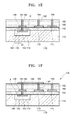
- FIGS. 1A through 1 F are diagrams for describing a method of manufacturing a three-dimensional monolithic electronic-photonic integrated circuit 100 step-by-step according to an example embodiment.
- a wafer may be provided that includes a plurality of chip areas.
- a region included in one chip area is illustrated briefly in FIGS. 1A through 1 F and will be referred to as a first substrate 110.
- the first substrate 110 may be formed of silicon (Si) or an III-V group material.
- the first substrate 110 is also referred to as a support substrate.
- a photonic element region R1 on which a photonic element is to be formed is confined.
- a trench 112 is formed in the photonic element region R1. Formation of the trench 112 may use general photolithography processing and, therefore, will not be described in detail.
- the trench 112 may be formed to a depth that provides a space for receiving the photonic element described below.
- the trench 112 may be formed to have a depth of 100 nm or more.
- a second substrate 150 is provided.
- the second substrate 150 may be formed of Si or an III-V group material.
- a photonic element 160 is formed on a region corresponding to the photonic element region R1.
- a plurality of photonic elements may be formed on the first surface 150a, but in the current embodiment, one photonic element has been illustrated for convenience.
- p-doping and n-doping are performed, such that a surface region A of the second substrate 150 connected to the photonic element 160 may be doped with impurities. That is, the surface region A may be a conductive region.
- the photonic element 160 may be a laser diode, a light emitting diode, an optical modulator, a multiplexer, a demultiplexer, a photo diode, or a waveguide.
- the second substrate 150 is bonded onto the first substrate 110 in such a way that the photonic element 160 faces a bottom 112a of the trench 112.
- plasma bonding may be used for the bonding.
- the trench 112 forms a specific sealed space 114 by the bonding between the first substrate 110 and the second substrate 150, and the photonic element 160 is disposed in the space 114.
- the second substrate 150 is thinned to form a thinned second substrate 152 having a thickness T1 of about 10 nm - 200 nm.
- Thinning may include primarily performing mechanical grinding or wet chemical etching and then performing chemical mechanical polishing (CMP).
- An electronic element 170 is formed on a second surface 152b of the thinned second substrate 152.
- the second surface 152b faces opposite the first surface 152a with respect to the thinned second substrate 152.
- the electronic element 170 may be formed on a first region next to the photonic element region R1.
- the electronic element 170 may include a switching element 172 for the photonic element 160 and a complementary metal oxide semiconductor (CMOS) element 174 connected to the switching element 172.
- CMOS element 174 may be a dynamic random access memory (DRAM), a central processing unit (CPU), large scale integration (LSI), or a system-on-chip (SoC).
- DRAM dynamic random access memory
- CPU central processing unit
- LSI large scale integration
- SoC system-on-chip
- a via 153 is formed in the second substrate 152 and is filled with metal to form a first metal via 154.
- An electrode pad 156 is formed on the second substrate 152 to be connected to the first metal via 154.
- a via may be formed to a shallow depth and filled with metal to connect the metal via with the conductive region A. If the conductive region A is formed to reach the second surface 152b and contact the electrode pad 156, the photonic element 160 and the electrode pad 156 may be electrically connected by the conductive region A without a need to form the via and the via metal.
- an insulating layer 180 is formed on the second substrate 152.
- the insulating layer 180 may be a silicon oxide layer.
- the insulating layer 180 may be an interlayer dielectric.
- vias 182 which expose the electrode pad 156, the switching element 172, and the CMOS element 174, are formed in the insulating layer 180, and then the vias 182 are filled with metal to form a second metal via 184, a third metal via 185, and a fourth metal via 186.
- the metal vias 184 through 186 connect the photonic element 160 and the electronic elements 172 and 174 to an external power source.
- the insulating layer 180 may confine light and reduce a propagation loss.
- a metal interconnection 188 which connects the second metal via 184 connected to the photonic element 160 with the third metal via 185 connected to the switching element 172, is formed.
- a metal interconnection 188 which connects the second metal via 184 connected to the photonic element 160 with the third metal via 185 connected to the switching element 172, is formed.
- Processes shown in FIGS. 1 E and 1 F may be repeated with the formation of the electronic element 170, such that a plurality of insulating layers including metal vias may be formed, and an electrode pad between the adjacent insulating layers may be electrically connected to metal vias in the insulating layers thereon and thereunder.
- the photonic element 160 is disposed on one surface of the thinned second substrate 152, where the electronic element 170 is disposed on another surface of the thinned second substrate 152, and the photonic element 160 and the electronic element 170 are monolithically formed.
- the three-dimensional monolithic electronic-photonic integrated circuit 170 having such a structure provides an improved integration degree and a simplified manufacturing process.
- the space 114 formed under the photonic element 160 and the insulating layer 180 formed on the photonic element 160 confines light, thereby reducing a propagation loss.
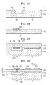
- FIGS. 2A through 2F are diagrams for describing a method of manufacturing a three-dimensional monolithic electronic-photonic integrated circuit step-by-step according to another example embodiment.
- a wafer is provided.
- the wafer includes a plurality of chip areas.
- a region included in one chip area is illustrated briefly, and will be referred to as a first substrate 210.
- the first substrate 210 may be formed of Si or an III-V group material.
- a photonic element region R1 on which a photonic element is to be formed and an electronic element region R2 on which an electronic element is to be formed are confined.
- another electronic element may also be formed on regions other than R1 and R2.
- a first trench 212 is formed on the photonic element region R1 of the first substrate 210.
- a depth D1 of the first trench 212 may be about 0.1 ⁇ m - about 3 ⁇ m. Formation of the first trench 212 may use a general photolithography process and will not be described in detail.
- the first trench 212 may be formed to a depth that provides a space for receiving a photonic element described below.
- a second trench 214 is formed in the photonic element region R2.
- a depth D2 of the second trench 214 may be about 1 nm - 200 nm such that electric charge leakage from the electronic circuit may be avoided while providing an efficient amount of heat emission and reduction in parasitic capacitance from the electronic circuit, such that a high-speed operation of the electronic circuit may be performed.
- Formation of the second trench 214 may use a general photolithography process and thus will not be described in detail.
- a second substrate 250 is provided.
- a photonic element 260 is formed on a region corresponding to the photonic element region R1.
- p-doping and n-doping are performed, such that a surface region A of the second substrate 250 connected to the photonic element 260 may be doped with impurities. That is, the surface region A may be a conductive region.
- the photonic element 260 may be a laser diode, a light emitting diode, an optical modulator, a multiplexer, a demultiplexer, a photo diode, or a waveguide.
- the second substrate 250 is bonded onto the first substrate 210 in such a way that the photonic element 260 faces a bottom 212a of the trench 212.
- the bonding may be performed using plasma bonding.
- the trench 212 forms a specific sealed space 216 by the bonding between the first substrate 210 and the second substrate 250, and the photonic element 260 is disposed in the space 216.
- the second substrate 250 is thinned to form a second substrate 252 having a thickness T1 of about 10 nm - 200 nm. Thinning may include primarily performing mechanical grinding or wet chemical etching and then performing CMP.
- an electronic element 270 is formed above the second trench 214.
- the photonic element 260 is formed on one surface of the second substrate 252, and the electronic element 270 is formed on another surface of the second substrate 252.
- the electronic element 270 may be formed on an electronic element region R2 next to the photonic element region R1.
- the electronic element 270 may include a switching element 272 for the photonic element 260 and a CMOS element 274 connected to the switching element 272.
- the CMOS element 274 may be a DRAM, a CPU, LSI, or a SoC.
- a via 253 is formed in the second substrate 252 and is filled with metal to form first metal via 254.
- An electrode pad 256 electrically connected to the first metal via 254 is formed on the second substrate 252.
- a via may be formed to a shallow depth and filled with metal to connect the metal via with the conductive region A. If the conductive region A is formed to contact the photonic element 260 and the electrode pad 256, the photonic element 260 and the electrode pad 256 may be electrically connected by the conductive region A without a need to form the via 253 and the metal via 254.
- an insulating layer 280 is formed on the second substrate 252.
- the insulating layer 280 may be a silicon oxide layer.
- the insulating layer 280 may be an interlayer dielectric.
- vias 282 which expose the electrode pad 256, the switching element 272, and the CMOS element 274, are formed in the insulating layer 280, and then the vias 282 are filled with metal to form a second metal via 284, a third metal via 285, and a fourth metal via 286.
- the insulating layer 280 may confine light and reduce a propagation loss.
- Processes shown in FIGS. 2E and 2F may be repeated with the formation of the electronic element 270 such that a plurality of insulating layers including metal vias may be formed, and an electrode pad between the adjacent insulating layers may be electrically connected to metal vias in the insulating layers thereon and thereunder.
- the first trench 212 and the insulating layer 280 may be formed to have thicknesses for optimizing performance of the photonic element 260, and the second trench 214 is formed for performance optimization of the electronic element 270, making it possible to achieve a high-speed operation of the electronic element 270 formed on the second trench 214.
- FIGS. 3A and 3B are diagrams for describing a method of manufacturing a three-dimensional monolithic electronic-photonic integrated circuit step-by-step according to still another example embodiment.
- an electronic element 370 is formed on a second substrate 352.
- the substrate 352 may have been thinned by performing mechanical grinding or wet chemical etching and then performing CMP to have a thickness T1 of about 10 nm - 200 nm.
- a via 353 may be formed on a photonic element 160 disposed in a surface region A, and the via 353 may be filled with metal to form a first metal via 354.
- the via 353 and the first metal via 354 may be omitted by extending the surface region A.
- the electronic element 370 may include a switching element 372 in a photonic element region R1 and a CMOS element 374 connected to the switching element 372 and the CMOS element 374 may be in a region next to the photonic element region R1.
- the CMOS element 374 may be a DRAM, a CPU, LSI, or a SoC.
- an insulating layer 380 is formed on the second substrate 352.
- the insulating layer 380 may be a silicon oxide layer.
- the insulating layer 380 may be an interlayer dielectric.
- vias 382 which expose the switching element 372 and the electronic element 374, are formed in the insulating layer 380, and then the vias 382 are filled with metal to form a second metal via 385 and a third metal via 386.
- the insulating layer 380 may confine light and reduces a propagation loss.
- FIG. 3B may be repeated with the formation of the electronic element 370 of FIG. 3A , and detailed description will be omitted.
- the second trench 214 shown in FIG. 2C may be further formed under the CMOS element 374 on the top surface of the first substrate 110, which will not be described herein.
Landscapes
- Optical Integrated Circuits (AREA)
- Light Receiving Elements (AREA)
- Optical Modulation, Optical Deflection, Nonlinear Optics, Optical Demodulation, Optical Logic Elements (AREA)
- Led Device Packages (AREA)
- Led Devices (AREA)
Applications Claiming Priority (1)
| Application Number | Priority Date | Filing Date | Title |
|---|---|---|---|
| KR1020130013487A KR20140100323A (ko) | 2013-02-06 | 2013-02-06 | 3차원 일체형 광전 집적회로 |
Publications (2)
| Publication Number | Publication Date |
|---|---|
| EP2765603A2 true EP2765603A2 (de) | 2014-08-13 |
| EP2765603A3 EP2765603A3 (de) | 2015-04-22 |
Family
ID=50031262
Family Applications (1)
| Application Number | Title | Priority Date | Filing Date |
|---|---|---|---|
| EP20140154000 Withdrawn EP2765603A3 (de) | 2013-02-06 | 2014-02-05 | Dreidimensionale, monolithische, elektronische-photonische integrierte Schaltung |
Country Status (5)
| Country | Link |
|---|---|
| US (1) | US20140217606A1 (de) |
| EP (1) | EP2765603A3 (de) |
| JP (1) | JP2014154884A (de) |
| KR (1) | KR20140100323A (de) |
| CN (1) | CN104022134A (de) |
Families Citing this family (6)
| Publication number | Priority date | Publication date | Assignee | Title |
|---|---|---|---|---|
| US9874693B2 (en) | 2015-06-10 | 2018-01-23 | The Research Foundation For The State University Of New York | Method and structure for integrating photonics with CMOs |
| US10078183B2 (en) | 2015-12-11 | 2018-09-18 | Globalfoundries Inc. | Waveguide structures used in phonotics chip packaging |
| KR20180090494A (ko) * | 2017-02-03 | 2018-08-13 | 삼성전자주식회사 | 기판 구조체 제조 방법 |
| CN109727915B (zh) * | 2017-10-30 | 2020-12-18 | 中芯国际集成电路制造(上海)有限公司 | 一种光子器件及其制造方法 |
| US11493713B1 (en) | 2018-09-19 | 2022-11-08 | Psiquantum, Corp. | Photonic quantum computer assembly having dies with specific contact configuration and matched CTE |
| DE102020102534A1 (de) * | 2020-01-31 | 2021-08-05 | Gesellschaft für angewandte Mikro- und Optoelektronik mit beschränkter Haftung - AMO GmbH | Halbleitervorrichtung und Halbleitereinrichtung sowie Verfahren zur Herstellung solcher |
Family Cites Families (4)
| Publication number | Priority date | Publication date | Assignee | Title |
|---|---|---|---|---|
| US6795120B2 (en) * | 1996-05-17 | 2004-09-21 | Sony Corporation | Solid-state imaging apparatus and camera using the same |
| US20080173792A1 (en) * | 2007-01-23 | 2008-07-24 | Advanced Chip Engineering Technology Inc. | Image sensor module and the method of the same |
| WO2011030428A1 (ja) * | 2009-09-10 | 2011-03-17 | 株式会社 東芝 | 赤外線撮像素子 |
| JP5786273B2 (ja) * | 2009-12-28 | 2015-09-30 | オムロン株式会社 | 赤外線センサ及び赤外線センサモジュール |
-
2013
- 2013-02-06 KR KR1020130013487A patent/KR20140100323A/ko not_active Withdrawn
-
2014
- 2014-02-05 EP EP20140154000 patent/EP2765603A3/de not_active Withdrawn
- 2014-02-05 JP JP2014020151A patent/JP2014154884A/ja active Pending
- 2014-02-06 US US14/173,888 patent/US20140217606A1/en not_active Abandoned
- 2014-02-07 CN CN201410044819.8A patent/CN104022134A/zh active Pending
Non-Patent Citations (1)
| Title |
|---|
| None |
Also Published As
| Publication number | Publication date |
|---|---|
| JP2014154884A (ja) | 2014-08-25 |
| CN104022134A (zh) | 2014-09-03 |
| KR20140100323A (ko) | 2014-08-14 |
| EP2765603A3 (de) | 2015-04-22 |
| US20140217606A1 (en) | 2014-08-07 |
Similar Documents
| Publication | Publication Date | Title |
|---|---|---|
| US9711502B2 (en) | Double-side process silicon MOS and passive devices for RF front-end modules | |
| US7626257B2 (en) | Semiconductor devices and methods of manufacture thereof | |
| EP2765603A2 (de) | Dreidimensionale, monolithische, elektronische-photonische integrierte Schaltung | |
| US8120110B2 (en) | Semiconductor structure including a high performance FET and a high voltage FET on a SOI substrate | |
| US10090327B2 (en) | Semiconductor device and method for forming the same | |
| US20130299950A1 (en) | Semiconductor structure with buried through substrate vias | |
| KR102007258B1 (ko) | 광전 집적회로 기판의 제조방법 | |
| KR20160134645A (ko) | 선택적 비아 포스트들을 갖는 스케일러블 인터커넥트 구조체들 | |
| KR20110136298A (ko) | 수직 채널 트랜지스터를 구비한 반도체 소자 및 그 제조 방법 | |
| US20100035430A1 (en) | Method of making through wafer vias | |
| US9559192B1 (en) | Method of fabricating semiconductor device | |
| KR102198344B1 (ko) | 3 차원 적층 소자 제조 방법 | |
| KR102869685B1 (ko) | 차폐 구조를 구비한 반도체 디바이스 | |
| KR20160039741A (ko) | 반도체 소자 및 그 형성방법 | |
| JP2025504616A (ja) | 埋め込み電源配線を有する半導体構造体 | |
| CN119318020A (zh) | 包括通过贯通电介质通孔耦合的堆叠管芯的微电子组装件 | |
| KR20150104928A (ko) | 반도체 장치 및 그 제조 방법 | |
| CN112582375B (zh) | 带侧壁互连结构的半导体装置及其制造方法及电子设备 | |
| US9478464B2 (en) | Method for manufacturing through-hole silicon via | |
| CN119028978A (zh) | 集成电路结构及其制造方法 | |
| EP4686336A1 (de) | Halbleiteranordnungen | |
| EP4535411B1 (de) | Verfahren zum dünnen eines halbleitersubstrats | |
| KR101679684B1 (ko) | 반도체 소자의 제조방법 | |
| CN109560065A (zh) | 一种带体接触的半导体器件结构和形成方法 | |
| US20240397701A1 (en) | Semiconductor devices |
Legal Events
| Date | Code | Title | Description |
|---|---|---|---|
| PUAI | Public reference made under article 153(3) epc to a published international application that has entered the european phase |
Free format text: ORIGINAL CODE: 0009012 |
|
| 17P | Request for examination filed |
Effective date: 20140205 |
|
| AK | Designated contracting states |
Kind code of ref document: A2 Designated state(s): AL AT BE BG CH CY CZ DE DK EE ES FI FR GB GR HR HU IE IS IT LI LT LU LV MC MK MT NL NO PL PT RO RS SE SI SK SM TR |
|
| AX | Request for extension of the european patent |
Extension state: BA ME |
|
| PUAL | Search report despatched |
Free format text: ORIGINAL CODE: 0009013 |
|
| AK | Designated contracting states |
Kind code of ref document: A3 Designated state(s): AL AT BE BG CH CY CZ DE DK EE ES FI FR GB GR HR HU IE IS IT LI LT LU LV MC MK MT NL NO PL PT RO RS SE SI SK SM TR |
|
| AX | Request for extension of the european patent |
Extension state: BA ME |
|
| RIC1 | Information provided on ipc code assigned before grant |
Ipc: H01L 27/146 20060101ALI20150319BHEP Ipc: H01L 27/00 20060101AFI20150319BHEP Ipc: H01L 31/18 20060101ALI20150319BHEP |
|
| R17P | Request for examination filed (corrected) |
Effective date: 20151022 |
|
| RBV | Designated contracting states (corrected) |
Designated state(s): AL AT BE BG CH CY CZ DE DK EE ES FI FR GB GR HR HU IE IS IT LI LT LU LV MC MK MT NL NO PL PT RO RS SE SI SK SM TR |
|
| STAA | Information on the status of an ep patent application or granted ep patent |
Free format text: STATUS: THE APPLICATION IS DEEMED TO BE WITHDRAWN |
|
| 18D | Application deemed to be withdrawn |
Effective date: 20151023 |