EP2765612A1 - Ga2o3-halbleiterlement - Google Patents
Ga2o3-halbleiterlement Download PDFInfo
- Publication number
- EP2765612A1 EP2765612A1 EP12829607.6A EP12829607A EP2765612A1 EP 2765612 A1 EP2765612 A1 EP 2765612A1 EP 12829607 A EP12829607 A EP 12829607A EP 2765612 A1 EP2765612 A1 EP 2765612A1
- Authority
- EP
- European Patent Office
- Prior art keywords
- single crystal
- crystal film
- type
- electrode
- semiconductor element
- Prior art date
- Legal status (The legal status is an assumption and is not a legal conclusion. Google has not performed a legal analysis and makes no representation as to the accuracy of the status listed.)
- Granted
Links
Images



Classifications
-
- H—ELECTRICITY
- H10—SEMICONDUCTOR DEVICES; ELECTRIC SOLID-STATE DEVICES NOT OTHERWISE PROVIDED FOR
- H10D—INORGANIC ELECTRIC SEMICONDUCTOR DEVICES
- H10D30/00—Field-effect transistors [FET]
-
- H—ELECTRICITY
- H10—SEMICONDUCTOR DEVICES; ELECTRIC SOLID-STATE DEVICES NOT OTHERWISE PROVIDED FOR
- H10D—INORGANIC ELECTRIC SEMICONDUCTOR DEVICES
- H10D30/00—Field-effect transistors [FET]
- H10D30/60—Insulated-gate field-effect transistors [IGFET]
-
- H—ELECTRICITY
- H10—SEMICONDUCTOR DEVICES; ELECTRIC SOLID-STATE DEVICES NOT OTHERWISE PROVIDED FOR
- H10D—INORGANIC ELECTRIC SEMICONDUCTOR DEVICES
- H10D30/00—Field-effect transistors [FET]
- H10D30/60—Insulated-gate field-effect transistors [IGFET]
- H10D30/64—Double-diffused metal-oxide semiconductor [DMOS] FETs
- H10D30/65—Lateral DMOS [LDMOS] FETs
-
- H—ELECTRICITY
- H10—SEMICONDUCTOR DEVICES; ELECTRIC SOLID-STATE DEVICES NOT OTHERWISE PROVIDED FOR
- H10D—INORGANIC ELECTRIC SEMICONDUCTOR DEVICES
- H10D30/00—Field-effect transistors [FET]
- H10D30/60—Insulated-gate field-effect transistors [IGFET]
- H10D30/64—Double-diffused metal-oxide semiconductor [DMOS] FETs
- H10D30/65—Lateral DMOS [LDMOS] FETs
- H10D30/657—Lateral DMOS [LDMOS] FETs having substrates comprising insulating layers, e.g. SOI-LDMOS transistors
-
- H—ELECTRICITY
- H10—SEMICONDUCTOR DEVICES; ELECTRIC SOLID-STATE DEVICES NOT OTHERWISE PROVIDED FOR
- H10D—INORGANIC ELECTRIC SEMICONDUCTOR DEVICES
- H10D30/00—Field-effect transistors [FET]
- H10D30/60—Insulated-gate field-effect transistors [IGFET]
- H10D30/67—Thin-film transistors [TFT]
- H10D30/6729—Thin-film transistors [TFT] characterised by the electrodes
-
- H—ELECTRICITY
- H10—SEMICONDUCTOR DEVICES; ELECTRIC SOLID-STATE DEVICES NOT OTHERWISE PROVIDED FOR
- H10D—INORGANIC ELECTRIC SEMICONDUCTOR DEVICES
- H10D30/00—Field-effect transistors [FET]
- H10D30/60—Insulated-gate field-effect transistors [IGFET]
- H10D30/67—Thin-film transistors [TFT]
- H10D30/674—Thin-film transistors [TFT] characterised by the active materials
- H10D30/6755—Oxide semiconductors, e.g. zinc oxide, copper aluminium oxide or cadmium stannate
-
- H—ELECTRICITY
- H10—SEMICONDUCTOR DEVICES; ELECTRIC SOLID-STATE DEVICES NOT OTHERWISE PROVIDED FOR
- H10D—INORGANIC ELECTRIC SEMICONDUCTOR DEVICES
- H10D30/00—Field-effect transistors [FET]
- H10D30/60—Insulated-gate field-effect transistors [IGFET]
- H10D30/67—Thin-film transistors [TFT]
- H10D30/6758—Thin-film transistors [TFT] characterised by the insulating substrates
-
- H—ELECTRICITY
- H10—SEMICONDUCTOR DEVICES; ELECTRIC SOLID-STATE DEVICES NOT OTHERWISE PROVIDED FOR
- H10D—INORGANIC ELECTRIC SEMICONDUCTOR DEVICES
- H10D30/00—Field-effect transistors [FET]
- H10D30/80—FETs having rectifying junction gate electrodes
- H10D30/87—FETs having Schottky gate electrodes, e.g. metal-semiconductor FETs [MESFET]
-
- H—ELECTRICITY
- H10—SEMICONDUCTOR DEVICES; ELECTRIC SOLID-STATE DEVICES NOT OTHERWISE PROVIDED FOR
- H10D—INORGANIC ELECTRIC SEMICONDUCTOR DEVICES
- H10D30/00—Field-effect transistors [FET]
- H10D30/80—FETs having rectifying junction gate electrodes
- H10D30/87—FETs having Schottky gate electrodes, e.g. metal-semiconductor FETs [MESFET]
- H10D30/875—FETs having Schottky gate electrodes, e.g. metal-semiconductor FETs [MESFET] having thin-film semiconductor bodies
-
- H—ELECTRICITY
- H10—SEMICONDUCTOR DEVICES; ELECTRIC SOLID-STATE DEVICES NOT OTHERWISE PROVIDED FOR
- H10D—INORGANIC ELECTRIC SEMICONDUCTOR DEVICES
- H10D62/00—Semiconductor bodies, or regions thereof, of devices having potential barriers
- H10D62/40—Crystalline structures
-
- H—ELECTRICITY
- H10—SEMICONDUCTOR DEVICES; ELECTRIC SOLID-STATE DEVICES NOT OTHERWISE PROVIDED FOR
- H10D—INORGANIC ELECTRIC SEMICONDUCTOR DEVICES
- H10D62/00—Semiconductor bodies, or regions thereof, of devices having potential barriers
- H10D62/40—Crystalline structures
- H10D62/405—Orientations of crystalline planes
-
- H—ELECTRICITY
- H10—SEMICONDUCTOR DEVICES; ELECTRIC SOLID-STATE DEVICES NOT OTHERWISE PROVIDED FOR
- H10D—INORGANIC ELECTRIC SEMICONDUCTOR DEVICES
- H10D62/00—Semiconductor bodies, or regions thereof, of devices having potential barriers
- H10D62/60—Impurity distributions or concentrations
-
- H—ELECTRICITY
- H10—SEMICONDUCTOR DEVICES; ELECTRIC SOLID-STATE DEVICES NOT OTHERWISE PROVIDED FOR
- H10D—INORGANIC ELECTRIC SEMICONDUCTOR DEVICES
- H10D62/00—Semiconductor bodies, or regions thereof, of devices having potential barriers
- H10D62/60—Impurity distributions or concentrations
- H10D62/605—Planar doped, e.g. atomic-plane doped or delta-doped
-
- H—ELECTRICITY
- H10—SEMICONDUCTOR DEVICES; ELECTRIC SOLID-STATE DEVICES NOT OTHERWISE PROVIDED FOR
- H10D—INORGANIC ELECTRIC SEMICONDUCTOR DEVICES
- H10D62/00—Semiconductor bodies, or regions thereof, of devices having potential barriers
- H10D62/80—Semiconductor bodies, or regions thereof, of devices having potential barriers characterised by the materials
-
- H—ELECTRICITY
- H10—SEMICONDUCTOR DEVICES; ELECTRIC SOLID-STATE DEVICES NOT OTHERWISE PROVIDED FOR
- H10D—INORGANIC ELECTRIC SEMICONDUCTOR DEVICES
- H10D62/00—Semiconductor bodies, or regions thereof, of devices having potential barriers
- H10D62/80—Semiconductor bodies, or regions thereof, of devices having potential barriers characterised by the materials
- H10D62/81—Semiconductor bodies, or regions thereof, of devices having potential barriers characterised by the materials of structures exhibiting quantum-confinement effects, e.g. single quantum wells; of structures having periodic or quasi-periodic potential variation
- H10D62/815—Semiconductor bodies, or regions thereof, of devices having potential barriers characterised by the materials of structures exhibiting quantum-confinement effects, e.g. single quantum wells; of structures having periodic or quasi-periodic potential variation of structures having periodic or quasi-periodic potential variation, e.g. superlattices or multiple quantum wells [MQW]
- H10D62/8171—Doping structures, e.g. doping superlattices or nipi superlattices
-
- H—ELECTRICITY
- H10—SEMICONDUCTOR DEVICES; ELECTRIC SOLID-STATE DEVICES NOT OTHERWISE PROVIDED FOR
- H10D—INORGANIC ELECTRIC SEMICONDUCTOR DEVICES
- H10D99/00—Subject matter not provided for in other groups of this subclass
-
- H—ELECTRICITY
- H10—SEMICONDUCTOR DEVICES; ELECTRIC SOLID-STATE DEVICES NOT OTHERWISE PROVIDED FOR
- H10P—GENERIC PROCESSES OR APPARATUS FOR THE MANUFACTURE OR TREATMENT OF DEVICES COVERED BY CLASS H10
- H10P14/00—Formation of materials, e.g. in the shape of layers or pillars
- H10P14/20—Formation of materials, e.g. in the shape of layers or pillars of semiconductor materials
- H10P14/22—Formation of materials, e.g. in the shape of layers or pillars of semiconductor materials using physical deposition, e.g. vacuum deposition or sputtering
-
- H—ELECTRICITY
- H10—SEMICONDUCTOR DEVICES; ELECTRIC SOLID-STATE DEVICES NOT OTHERWISE PROVIDED FOR
- H10P—GENERIC PROCESSES OR APPARATUS FOR THE MANUFACTURE OR TREATMENT OF DEVICES COVERED BY CLASS H10
- H10P14/00—Formation of materials, e.g. in the shape of layers or pillars
- H10P14/20—Formation of materials, e.g. in the shape of layers or pillars of semiconductor materials
- H10P14/29—Formation of materials, e.g. in the shape of layers or pillars of semiconductor materials characterised by the substrates
- H10P14/2901—Materials
- H10P14/2918—Materials being semiconductor metal oxides
-
- H—ELECTRICITY
- H10—SEMICONDUCTOR DEVICES; ELECTRIC SOLID-STATE DEVICES NOT OTHERWISE PROVIDED FOR
- H10P—GENERIC PROCESSES OR APPARATUS FOR THE MANUFACTURE OR TREATMENT OF DEVICES COVERED BY CLASS H10
- H10P14/00—Formation of materials, e.g. in the shape of layers or pillars
- H10P14/20—Formation of materials, e.g. in the shape of layers or pillars of semiconductor materials
- H10P14/29—Formation of materials, e.g. in the shape of layers or pillars of semiconductor materials characterised by the substrates
- H10P14/2926—Crystal orientations
-
- H—ELECTRICITY
- H10—SEMICONDUCTOR DEVICES; ELECTRIC SOLID-STATE DEVICES NOT OTHERWISE PROVIDED FOR
- H10P—GENERIC PROCESSES OR APPARATUS FOR THE MANUFACTURE OR TREATMENT OF DEVICES COVERED BY CLASS H10
- H10P14/00—Formation of materials, e.g. in the shape of layers or pillars
- H10P14/20—Formation of materials, e.g. in the shape of layers or pillars of semiconductor materials
- H10P14/34—Deposited materials, e.g. layers
- H10P14/3402—Deposited materials, e.g. layers characterised by the chemical composition
- H10P14/3434—Deposited materials, e.g. layers characterised by the chemical composition being oxide semiconductor materials
-
- H—ELECTRICITY
- H10—SEMICONDUCTOR DEVICES; ELECTRIC SOLID-STATE DEVICES NOT OTHERWISE PROVIDED FOR
- H10P—GENERIC PROCESSES OR APPARATUS FOR THE MANUFACTURE OR TREATMENT OF DEVICES COVERED BY CLASS H10
- H10P14/00—Formation of materials, e.g. in the shape of layers or pillars
- H10P14/20—Formation of materials, e.g. in the shape of layers or pillars of semiconductor materials
- H10P14/34—Deposited materials, e.g. layers
- H10P14/3438—Doping during depositing
- H10P14/3441—Conductivity type
- H10P14/3442—N-type
-
- H—ELECTRICITY
- H10—SEMICONDUCTOR DEVICES; ELECTRIC SOLID-STATE DEVICES NOT OTHERWISE PROVIDED FOR
- H10P—GENERIC PROCESSES OR APPARATUS FOR THE MANUFACTURE OR TREATMENT OF DEVICES COVERED BY CLASS H10
- H10P14/00—Formation of materials, e.g. in the shape of layers or pillars
- H10P14/20—Formation of materials, e.g. in the shape of layers or pillars of semiconductor materials
- H10P14/34—Deposited materials, e.g. layers
- H10P14/3438—Doping during depositing
- H10P14/3441—Conductivity type
- H10P14/3446—Transition metal elements; Rare earth elements
Definitions
- the invention relates to a Ga 2 O 3 -based semiconductor element.
- a Ga 2 O 3 -based semiconductor element using a Ga 2 O 3 crystal film formed on a sapphire substrate is known (see, e.g., NPLs 1 and 2 ).
- Ga 2 O 3 crystal since the crystal structure of Ga 2 O 3 crystal is completely different from that of sapphire crystal, it is very difficult to heteroepitaxially grow a Ga 2 O 3 crystal on a sapphire substrate. Thus, it is difficult to form a high-quality Ga 2 O 3 -based semiconductor element by using a Ga 2 O 3 crystal film grown on a sapphire substrate.
- a Ga 2 O 3 -based semiconductor element as defined in [ 1 ] to [ 6 ] below is provided so as to achieve the above object.
- a high-quality Ga 2 O 3 -based semiconductor element can be provided.
- ⁇ -Ga 2 O 3 -based single crystal film it is possible to form a high-quality ⁇ -Ga 2 O 3 -based single crystal film by homoepitaxial growth and use of such a high-quality ⁇ -Ga 2 O 3 -based single crystal film allows a high-quality Ga 2 O 3 -based semiconductor element to be formed. Examples of embodiments thereof will be described in detail below.
- Ga 2 O 3 -based MISFET Metal Insulator Semiconductor Field Effect Transistor
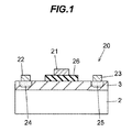
- FIG.1 is a cross sectional view showing a Ga 2 O 3 -based MISFET 20 in the first embodiment.
- the Ga 2 O 3 -based MISFET 20 includes an n-type ⁇ -Ga 2 O 3 single crystal film 3 formed on a high-resistance ⁇ -Ga 2 O 3 substrate 2, a source electrode 22 and a drain electrode 23 which are formed on the n-type ⁇ -Ga 2 O 3 single crystal film 3, a gate electrode 21 formed on the n-type ⁇ -Ga 2 O 3 single crystal film 3 between the source electrode 22 and the drain electrode 23 via a gate insulating film 26, and a source region 24 and a drain region 25 which are formed in the n-type ⁇ -Ga 2 O 3 single crystal film 3 respectively under the source electrode 22 and the drain electrode 23.
- the high-resistance ⁇ -Ga 2 O 3 substrate 2 is a ⁇ -Ga 2 O 3 substrate of which resistance is increased by adding a p-type dopant such as Mg, H, Li, Na, K, Rb, Cs, Fr, Be, Ca, Sr, Ba, Ra, Mn, Fe, Co, Ni, Pd, Cu, Ag, Au, Zn, Cd, Hg, Tl, Pb, N or P.
- a p-type dopant such as Mg, H, Li, Na, K, Rb, Cs, Fr, Be, Ca, Sr, Ba, Ra, Mn, Fe, Co, Ni, Pd, Cu, Ag, Au, Zn, Cd, Hg, Tl, Pb, N or P.
- Plane orientation of the main surface of the high-resistance ⁇ -Ga 2 O 3 substrate 2 is not specifically limited but a plane rotated by not less than 50° and not more than 90° with respect a (100) plane is preferable.
- an angle ⁇ (0 ⁇ 90 °) formed between the main surface and the (100) plane is preferably not less than 50°.
- Examples of the plane rotated by not less than 50° and not more than 90° with respect the (100) plane include a (010) plane, a (001) plane, a (-201) plane, a (101) plane and a (310) plane.
- the main surface of the high-resistance ⁇ -Ga 2 O 3 substrate 2 is a plane rotated by not less than 50° and not more than 90° with respect the (100) plane, it is possible to effectively suppress re-evaporation of raw materials of the ⁇ -Ga 2 O 3 -based crystal from the high-resistance ⁇ -Ga 2 O 3 substrate 2 at the time of epitaxially growing the ⁇ -Ga 2 O 3 -based crystal on the high-resistance ⁇ -Ga 2 O 3 substrate 2.
- the percentage of the re-evaporated raw material during growth of the ⁇ -Ga 2 O 3 -based crystal at a growth temperature of 500°C can be suppressed to not more than 40% when the main surface of the high-resistance ⁇ -Ga 2 O 3 substrate 2 is a plane rotated by not less than 50° and not more than 90° with respect the (100) plane. It is thus possible to use not less than 60% of the supplied raw material to form the ⁇ -Ga 2 O 3 -based crystal, which is preferable from the viewpoint of growth rate and manufacturing cost of the ⁇ -Ga 2 O 3 -based crystal.
- the (100) plane comes to coincide with the (310) plane when rotated by 52.5° around the c-axis and comes to coincide with the (010) plane when rotated by 90°.
- the (100) plane comes to coincide with the (101) plane when rotated by 53.8° around the b-axis, comes to coincide with the (001) plane when rotated by 76.3° and comes to coincide with the (-201) plane when rotated by 53.8°.
- the main surface of the high-resistance ⁇ -Ga 2 O 3 substrate 2 may be a plane rotated at an angle of not more than 37.5° with respect to the (010) plane. In this case, it is possible to provide a steep interface between the high-resistance ⁇ -Ga 2 O 3 substrate 2 and the n-type ⁇ -Ga 2 O 3 single crystal film 3 and it is also possible to highly accurately control the thickness of the i-type ⁇ -Ga 2 O 3 single crystal film 3.
- the n-type ⁇ -Ga 2 O 3 single crystal film 3 is an electrically conductive single crystal film formed on the high-resistance ⁇ -Ga 2 O 3 substrate 2 by the below-described method.
- the n-type ⁇ -Ga 2 O 3 single crystal film 3 includes an n-type dopant such as Sn, Ti, Zr, Hf, V, Nb, Ta, Mo, W, Ru, Rh, Ir, C, Si, Ge, Pb, Mn, As, Sb, Bi, F, Cl, Br and I.
- the thickness of the n-type ⁇ -Ga 2 O 3 single crystal film 3 is, e.g., about 10 to 1000 nm.
- another film such as a non-doped ⁇ -Ga 2 O 3 single crystal film may be formed between the high-resistance ⁇ -Ga 2 O 3 substrate 2 and the n-type ⁇ -Ga 2 O 3 single crystal film 3.
- the non-doped ⁇ -Ga 2 O 3 single crystal film is formed on the high-resistance ⁇ -Ga 2 O 3 substrate 2 by homoepitaxial growth and the n-type ⁇ -Ga 2 O 3 single crystal film 3 is formed on the non-doped ⁇ -Ga 2 O 3 single crystal film by homoepitaxial growth.
- the gate electrode 21, the source electrode 22 and the drain electrode 23 are formed of, e.g., a metal such as Au, Al, Ti, Sn, Ge, In, Ni, Co, Pt, W, Mo, Cr, Cu and Pb, an alloy containing two or more of such metals, or a conductive compound such as ITO.
- the structure thereof may be a two-layer structure composed of two different metals, e.g., Al/Ti, Au/Ni or Au/Co.
- the gate insulating film 26 is formed of an insulating material such as SiO 2 , AIN, SiN, Al 2 O 3 or ⁇ -(Al x Ga 1-x ) 2 O 3 ( 0 ⁇ x ⁇ 1 ).
- ⁇ -(Al x Ga 1-x ) 2 O 3 can be grown as a single crystal film on a ⁇ -Ga 2 O 3 crystal and thus allows a good semiconductor/insulating film interface with less interface states to be formed, resulting in better gate characteristics than when using other insulating films.
- the source region 24 and the drain region 25 are regions having a high n-type dopant concentration formed in the n-type ⁇ -Ga 2 O 3 single crystal film 3 and are respectively connected to the source electrode 22 and the drain electrode 23. It should be noted that the source region 24 and the drain region 25 do not need to be provided in the Ga 2 O 3 -based MISFET 20.
- the Ga 2 O 3 -based MISFET 20 is a normally-on transistor.
- the source electrode 22 is electrically connected to the drain electrode 23 via the n-type ⁇ -Ga 2 O 3 single crystal film 3. Therefore, if a voltage is applied between the source electrode 22 and the drain electrode 23 without applying a voltage to the gate electrode 21, a current flows from the source electrode 22 to the drain electrode 23.
- an inversion layer is formed in the n-type ⁇ -Ga 2 O 3 single crystal film 3 in a region under the gate electrode 21 and a current does not flow from the source electrode 22 to the drain electrode 23 even when voltage is applied between the source electrode 22 and the drain electrode 23.
- the method of manufacturing the ⁇ -Ga 2 O 3 -based single crystal film is PLD (Pulsed Laser Deposition), CVD (Chemical Vapor Deposition), sputtering and MBE (Molecular Beam Epitaxy) etc.
- a thin film growth method using the MBE is employed.
- the MBE is a crystal growth method in which a single or compound solid is heated in an evaporation source called cell and vapor generated by heat is supplied as a molecular beam onto the surface of the substrate.
- FIG.2 is a structural diagram illustrating an example MBE system used for forming the ⁇ -Ga 2 O 3 -based single crystal film.
- the MBE system 1 is provided with a vacuum chamber 10, a substrate holder 11 supported in the vacuum chamber 10 to hold the high-resistance ⁇ -Ga 2 O 3 substrate 2, heating devices 12 held on the substrate holder 11 to heat the high-resistance ⁇ -Ga 2 O 3 substrate 2, plural cells 13 ( 13 a, 13 b) each provided for each atom or molecule constituting a thin film, heaters 14 ( 14 a, 14 b) for hearing the plural cells 13, a gas supply pipe 15 for supplying oxygen-based gas into the vacuum chamber 10, and a vacuum pump 16 for exhausting the air in the vacuum chamber 10.
- the substrate holder 11 can be rotated by a non-illustrated motor via a shaft 110.
- the Ga powder desirably has a purity of not less than 6N.
- Powder of an n-type dopant raw material to be doped as a donor is loaded in the second cell 13 b.
- a shutter is provided at an opening of each of the first cell 13 a and the second cell 13 b.
- the preliminarily-formed high-resistance ⁇ -Ga 2 O 3 substrate 2 is attached to the substrate holder 11 and a ⁇ -Ga 2 O 3 crystal is then homoepitaxially grown on the high-resistance ⁇ -Ga 2 O 3 substrate 2 while adding an n-type dopant, thereby forming the n-type ⁇ -Ga 2 O 3 single crystal film 3.
- the high-resistance ⁇ -Ga 2 O 3 substrate 2 is made by, e.g., the following procedure. Firstly, a semi-insulating ⁇ -Ga 2 O 3 single crystal ingot doped with Mg is made by the EFG (edge-defined film-fed growth) method. It should be noted that an element to be doped is not limited to Mg.
- an element to be doped is not limited to Mg.
- MgO powder is mixed to raw material powder. Not less than 0.05 mol% of MgO is added to impart good insulation properties to the high-resistance ⁇ -Ga 2 O 3 substrate 2.
- the semi-insulating ⁇ -Ga 2 O 3 single crystal ingot may be made by the FZ (floating zone) method.
- the obtained ingot is sliced to a thickness of, e.g., about 1 mm so that the main surface has a desired plane orientation, thereby forming a substrate.
- a grinding and polishing process is performed to a thickness of about 300 to 600 ⁇ m.
- the high-resistance ⁇ -Ga 2 O 3 substrate 2 made by the above procedure is attached to the substrate holder 11 of the MBE system 1.
- the vacuum pump 16 is activated to reduce atmospheric pressure in the vacuum chamber 10 to about 10 -10 Torr.
- the high-resistance ⁇ -Ga 2 O 3 substrate 2 is heated by the heating devices 12.
- radiation heat of heat source such as graphite heater of the heating device 12 is thermally transferred to the high-resistance ⁇ -Ga 2 O 3 substrate 2 via the substrate holder 11 and the high-resistance ⁇ -Ga 2 O 3 substrate 2 is thereby heated.
- oxygen-based gas is supplied into the vacuum chamber 10 through the gas supply pipe 15.
- the first cell 13 a and the second cell 13 b are respectively heated by the first heater 14 a and the second heater 14 b while rotating the substrate holder 11 so that Ga and n-type dopant are evaporated and are radiated as molecular beam onto the surface of the high-resistance ⁇ -Ga 2 O 3 substrate 2.
- the first cell 13 a is heated to 900°C and beam-equivalent pressure (BEP) of Ga vapor is 1x10 -4 Pa.
- BEP beam-equivalent pressure
- the ⁇ -Ga 2 O 3 crystal is homoepitaxially grown on the main surface of the high-resistance ⁇ -Ga 2 O 3 substrate 2 while being doped with the n-type dopant such as Sn and the n-type ⁇ -Ga 2 O 3 single crystal film 3 is thereby formed.
- Growth temperature of the ⁇ -Ga 2 O 3 crystal is e.g., 700°C.
- n-type dopant other than Sn it is possible to use Ti, Zr, Hf, V, Nb, Ta, Mo, W, Ru, Rh, Ir, C, Si, Ge, Pb, Mn, As, Sb and Bi, etc., for substituting Ga site and it is possible to use F, Cl, Br and I, etc., for substituting oxygen site.
- the n-type ⁇ -Ga 2 O 3 single crystal film 3 may be formed by the PLD (Pulsed Laser Deposition) or the CVD (Chemical Vapor Deposition) etc.
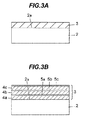
- FIGS.3A and 3B are cross sectional views showing the n-type ⁇ -Ga 2 O 3 single crystal film 3 in the present embodiment.
- the n-type ⁇ -Ga 2 O 3 single crystal film 3 is formed on a main surface 2 a of the high-resistance ⁇ -Ga 2 O 3 substrate 2 by the MBE mentioned above.
- FIG.3A shows the n-type ⁇ -Ga 2 O 3 single crystal film 3 which is formed by continuously adding the n-type dopant during homoepitaxial growth of the ⁇ -Ga 2 O 3 crystal.
- the donor concentration in the n-type ⁇ -Ga 2 O 3 single crystal film 3 is, e.g., 1x10 15 to 1x10 19 /cm 3 and is especially preferably 1x10 17 to 1x10 18 /cm 3 .
- This donor concentration can be controlled by temperature of the second cell 13b during film formation.
- FIG.3B shows the n-type ⁇ -Ga 2 O 3 single crystal film 3 which is formed by intermittently adding the n-type dopant at certain intervals during homoepitaxial growth of the ⁇ -Ga 2 O 3 crystal.
- Sn is used as the n-type dopant.
- Sn vapor is intermittently generated from the second cell 13 b by operating the shutter of the second cell 13 b, thereby intermittently adding Sn to the ⁇ -Ga 2 O 3 single. It is preferable that Sn be intermittently added twice or more. In this case, electrical conductivity according to the added amount of Sn can be imparted to the n-type ⁇ -Ga 2 O 3 single crystal film 3 without performing annealing treatment.
- the n-type ⁇ -Ga 2 O 3 single crystal film 3 in FIG.3B has first layers 4 ( 4 a, 4 b, 4 c) grown during the period with no Sn addition and second layers 5 ( 5 a, 5 b, 5 c) grown during the period with Sn addition.
- the Sn concentration in the second layer 5 can be controlled by temperature of the second cell 13b during the film formation.
- An average Sn concentration in the n-type ⁇ -Ga 2 O 3 single crystal film 3 is, e.g., 1x10 14 to 3x10 18 /cm 3 and is especially preferably 1x10 17 to 1x10 18 /cm 3 .
- the first layers 4 a , 4 b and 4 c are 3 to 20 nm in thickness and the second layers 5 a, 5 b and 5c are 0.2 to 1 nm in thickness. If the thickness of the first layers 4 a, 4 b and 4 c is greater than 20 nm, the effect of providing the n-type may be reduced since intervals of the second layers 5 a, 5 b and 5 c are too large.
- the thickness of the second layers 5 a, 5 b and 5 c is greater than 1 nm, the effect of intermittently providing the n-type may be reduced since the amount of Sn diffused from the second layers 5 a, 5 b and 5 c into the first layers 4 a, 4 b and 4 c is too large.
- the lowermost layer of the n-type ⁇ -Ga 2 O 3 single crystal film 3 (the layer in contact with the main surface 2 a of the high-resistance ⁇ -Ga 2 O 3 substrate 2 ) may be either the first layer 4 or the second layer 5.
- the number of the first layers 4 and that of the second layers 5 are not limited.
- the source region 24 and the drain region 25 are formed by ion-implanting the n-type dopant such as Sn into the n-type ⁇ -Ga 2 O 3 single crystal film 3.
- the ion to be implanted is not limited to Sn and, when substituting, e.g., Ga site, it is possible to use Ti, Zr, Hf, V, Nb, Ta, Mo, W, Ru, Rh, Ir, C, Si, Ge, Pb, Mn, As, Sb or Bi.
- F, Cl, Br or I when substituting oxygen site.
- the implantation concentration is, e.g., not less than 1x10 18 /cm 3 and not more than 5x10 19 cm 3 .
- the implantation depth is not less than 30 nm.
- the surface of the implanted region is etched about 10 nm by hydrofluoric acid. Sulfuric acid, nitric acid or hydrochloric acid may be used instead.
- implantation damage is repaired by performing annealing treatment in a nitrogen atmosphere at not less than 800°C for not less than 30 minutes. In case of performing the annealing treatment in an oxygen atmosphere, treatment temperature is not less than 800°C and not more than 950°C and treatment time is not less than 30 minutes.
- the method of forming the source region 24 and the drain region 25 is not limited to ion implantation and thermal diffusion process may be used.
- metal such as Sn
- heat treatment is performed to diffuse a dopant such as Sn into the n-type ⁇ -Ga 2 O 3 single crystal film 3.
- the source region 24 and the drain region 25 do not need to be formed.
- the gate insulating film 26, the source electrode 22, the drain electrode 23 and the gate electrode 21 are formed.
- Ga 2 O 3 -based MESFET Metal Semiconductor Field Effect Transistor
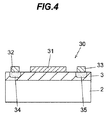
- FIG.4 is a cross sectional view showing a Ga 2 O 3 -based MESFET 30 in the second embodiment.
- the Ga 2 O 3 -based MESFET 30 includes the n-type ⁇ -Ga 2 O 3 single crystal film 3 formed on the high-resistance ⁇ -Ga 2 O 3 substrate 2, a source electrode 32 and a drain electrode 33 which are formed on the n-type ⁇ -Ga 2 O 3 single crystal film 3, a gate electrode 31 formed on the n-type ⁇ -Ga 2 O 3 single crystal film 3 between the source electrode 32 and the drain electrode 33, and a source region 34 and a drain region 35 which are formed in the n-type ⁇ -Ga 2 O 3 single crystal film 3 respectively under the source electrode 32 and the drain electrode 33.
- the structure and the manufacturing method of the high-resistance ⁇ -Ga 2 O 3 substrate 2 and those of the n-type ⁇ -Ga 2 O 3 single crystal film 3 are the same as the first embodiment.
- the gate electrode 31, the source electrode 32, the drain electrode 33, the source region 34 and the drain region 35 are formed in the same manner as the gate electrode 21, the source electrode 22, the drain electrode 23, the source region 24 and the drain region 25 in the first embodiment. It should be noted that the source region 34 and the drain region 35 do not need to be provided in the Ga 2 O 3 -based MESFET 30.
- the source electrode 32 is electrically connected to the drain electrode 33 via the n-type ⁇ -Ga 2 O 3 single crystal film 3. Meanwhile, a Schottky junction is formed at an interface between the gate electrode 31 and the n-type ⁇ -Ga 2 O 3 single crystal film 3 and a depletion layer is thus formed in the n-type ⁇ -Ga 2 O 3 single crystal film 3 under the gate electrode 31.
- the Ga 2 O 3 -based MESFET 30 functions as either a normally-off transistor or a normally-on transistor depending on the thickness of the depletion region.
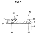
- FIG.5 is a cross sectional view showing a Ga 2 O 3 -based MISFET 40 in the third embodiment.
- the Ga 2 O 3 -based MISFET 40 includes the n-type ⁇ -Ga 2 O 3 single crystal film 3 formed on the high-resistance ⁇ -Ga 2 O 3 substrate 2, a source electrode 42 and a drain electrode 43 which are formed on the n-type ⁇ -Ga 2 O 3 single crystal film 3, a gate electrode 41 formed on the n-type ⁇ -Ga 2 O 3 single crystal film 3 between the source electrode 42 and the drain electrode 43 via a gate insulating film 46, a source region 44 and a drain region 45 which are formed in the n-type ⁇ -Ga 2 O 3 single crystal film 3 respectively under the source electrode 42 and the drain electrode 43, and a body region 47 surrounding the source region 44.
- the structure and the manufacturing method of the high-resistance ⁇ -Ga 2 O 3 substrate 2 and those of the n-type ⁇ -Ga 2 O 3 single crystal film 3 are the same as the first embodiment.
- the gate electrode 41, the source electrode 42, the drain electrode 43, the source region 44, the drain region 45 and the gate insulating film 46 are formed in the same manner as the gate electrode 21, the source electrode 22, the drain electrode 23, the source region 24, the drain region 25 and the gate insulating film 26 in the first embodiment. It should be noted that the source region 44 and the drain region 45 do not need to be provided in the Ga 2 O 3 -based MISFET 40.
- the body region 47 includes a p-type dopant such as Mg, H, Li, Na, K, Rb, Cs, Fr, Be, Ca, Sr, Ba, Ra, Mn, Fe, Co, Ni, Pd, Cu, Ag, Au, Zn, Cd, Hg, Tl, Pb, N or P.
- the body region 47 is a p-type region or a high resistance region which behaves like i-type due to charge compensation.
- the body region 47 is formed by ion-implanting a p-type dopant such as Mg into the n-type ⁇ -Ga 2 O 3 single crystal film 3.
- a p-type dopant such as Mg into the n-type ⁇ -Ga 2 O 3 single crystal film 3.
- the ion to be implanted is not limited to Mg and, when substituting, e.g., Ga site, it is possible to use H, Li, Na, K, Rb, Cs, Fr, Ca, Sr, Ba, Ra, Mn, Fe, Co, Ni, Pd, Cu, Ag, Au, Zn, Cd, Hg, Tl or Pb.
- N or P when substituting oxygen site.
- the method of forming the body region 47 is not limited to ion implantation and thermal diffusion process may be used.
- a metal film such as Mg film is brought into contact with the n-type ⁇ -Ga 2 O 3 single crystal film 3 in a region for the body region 47 to be formed, heat treatment is performed to diffuse a dopant such as Mg into the n-type ⁇ -Ga 2 O 3 single crystal film 3.
- the Ga 2 O 3 -based MISFET 40 functions as a normally-off transistor. In a state that voltage is not applied to the gate electrode 41, a current does not flow from the source electrode 42 to the drain electrode 43 due to the presence of the body region 47. When voltage of more than the threshold is applied to the gate electrode 41, a channel is formed in a region of the body region 47 under the gate electrode 41 and a current thus flows from the source electrode 42 to the drain electrode 43.
- FIG.6 is a cross sectional view showing a Ga 2 O 3 -based MISFET 50 in the fourth embodiment.
- the Ga 2 O 3 -based MISFET 50 includes an undoped ⁇ -Ga 2 O 3 single crystal film 6 formed on the high-resistance ⁇ -Ga 2 O 3 substrate 2, a source electrode 52 and a drain electrode 53 which are formed on the undoped ⁇ -Ga 2 O 3 single crystal film 6, a gate electrode 51 formed on the undoped ⁇ -Ga 2 O 3 single crystal film 6 between the source electrode 52 and the drain electrode 53 via a gate insulating film 56, and a source region 54 and a drain region 55 which are formed in the undoped ⁇ -Ga 2 O 3 single crystal film 6 respectively under the source electrode 52 and the drain electrode 53.
- the structure and the manufacturing method of the high-resistance ⁇ -Ga 2 O 3 substrate 2 are the same as the first embodiment.
- the gate electrode 51, the source electrode 52, the drain electrode 53, the source region 54, the drain region 55 and the gate insulating film 56 are formed in the same manner as the gate electrode 21, the source electrode 22, the drain electrode 23, the source region 24, the drain region 25 and the gate insulating film 26 in the first embodiment. It should be noted that the source region 54 and the drain region 55 do not need to be provided in the Ga 2 O 3 -based MISFET 50.
- the undoped ⁇ -Ga 2 O 3 single crystal film 6 is a high-resistance ⁇ -Ga 2 O 3 single crystal film which does not include a dopant. Although there may be a case where conductivity thereof is low due to crystal defects, etc., electric resistance thereof is sufficiently high and a current never flows from the source electrode 52 to the drain electrode 53 unless voltage is applied to the gate electrode 51.
- the method of forming the undoped ⁇ -Ga 2 O 3 single crystal film 6 is, e.g., based on the method of forming the n-type ⁇ -Ga 2 O 3 single crystal film 3 in the first embodiment where the process of implanting the n-type dopant is eliminated.
- the Ga 2 O 3 -based MISFET 50 functions as a normally-off transistor.
- voltage of more than the threshold is applied to the gate electrode 51, a channel is formed in a region of the undoped ⁇ -Ga 2 O 3 single crystal film 6 under the gate electrode 51 and a current thus flows from the source electrode 52 to the drain electrode 53.
- FIG.7 is a cross sectional view showing a Ga 2 O 3 -based MISFET 60 in the fifth embodiment.
- the Ga 2 O 3 -based MISFET 60 includes a p-type ⁇ -Ga 2 O 3 single crystal film 7 formed on the high-resistance ⁇ -Ga 2 O 3 substrate 2, a source electrode 62 and a drain electrode 63 which are formed on the p-type ⁇ -Ga 2 O 3 single crystal film 7, a gate electrode 61 formed on the p-type ⁇ -Ga 2 O 3 single crystal film 7 between the source electrode 62 and the drain electrode 63 via a gate insulating film 66, and a source region 64 and a drain region 65 which are formed in the p-type ⁇ -Ga 2 O 3 single crystal film 7 respectively under the source electrode 62 and the drain electrode 63.
- the structure and the manufacturing method of the high-resistance ⁇ -Ga 2 O 3 substrate 2 are the same as the first embodiment.
- the gate electrode 61, the source electrode 62, the drain electrode 63, the source region 64, the drain region 65 and the gate insulating film 66 are formed in the same manner as the gate electrode 21, the source electrode 22, the drain electrode 23, the source region 24, the drain region 25 and the gate insulating film 26 in the first embodiment.
- the p-type ⁇ -Ga 2 O 3 single crystal film 7 is a ⁇ -Ga 2 O 3 single crystal film which includes a p-type dopant such as Mg, H, Li, Na, K, Rb, Cs, Fr, Be, Ca, Sr, Ba, Ra, Mn, Fe, Co, Ni, Pd, Cu, Ag, Au, Zn, Cd, Hg, TI, Pb, N or P.
- a p-type dopant such as Mg, H, Li, Na, K, Rb, Cs, Fr, Be, Ca, Sr, Ba, Ra, Mn, Fe, Co, Ni, Pd, Cu, Ag, Au, Zn, Cd, Hg, TI, Pb, N or P.
- the method of forming the p-type ⁇ -Ga 2 O 3 single crystal film 7 is, e.g., based on the method of forming the n-type ⁇ -Ga 2 O 3 single crystal film 3 in the first embodiment where the process of implanting the n-type dopant is replaced with a process of implanting the p-type dopant.
- the Ga 2 O 3 -based MISFET 60 functions as a normally-off transistor.
- voltage of more than the threshold is applied to the gate electrode 61, a channel is formed in a region of the p-type ⁇ -Ga 2 O 3 single crystal film 7 under the gate electrode 61 and a current thus flows from the source electrode 62 to the drain electrode 63.
- ⁇ -Ga 2 O 3 single crystal films it is possible to form high-quality ⁇ -Ga 2 O 3 single crystal films by homoepitaxial growth and use of such ⁇ -Ga 2 O 3 single crystal films allows high-quality Ga 2 O 3 -based MISFETs or Ga 2 O 3 -based MESFETs to be formed.
- these Ga 2 O 3 -based MISFETs and Ga 2 O 3 -based MESFETs have excellent performance since a high-quality ⁇ -Ga 2 O 3 single crystal film is used as a channel layer.
- the Ga 2 O 3 -based MESFET 30 in the second embodiment was made and transistor characteristics thereof were evaluated.
- ⁇ -Ga 2 O 3 -based single crystal was then grown by the FZ method.
- the high-resistance ⁇ -Ga 2 O 3 substrate 2 was cut out of the grown ⁇ -Ga 2 O 3 -based single crystal so as to have a (010) plane as a main surface and was ground and polished to a thickness of about 350 ⁇ m.
- the high-resistance ⁇ -Ga 2 O 3 substrate 2 was subjected to organic cleaning, acid cleaning and pure water cleaning and was then conveyed to the MBE system.
- an n-type ⁇ -Ga 2 O 3 single crystal was grown on the high-resistance ⁇ -Ga 2 O 3 substrate 2 by the MBE to form the n-type ⁇ -Ga 2 O 3 single crystal film 3.
- temperature of the high-resistance ⁇ -Ga 2 O 3 substrate 2 was set to 700°C
- temperature of the first cell 13 a filled with Ga powder to 900°C and temperature of the second cell 13 b filled with SnO 2 powder to 770°C and the n-type ⁇ -Ga 2 O 3 single crystal was grown for 30 minutes, thereby forming the n-type ⁇ -Ga 2 O 3 single crystal film 3 having a thickness of 0.3 ⁇ m.
- the Sn concentration in the n-type ⁇ -Ga 2 O 3 single crystal film 3 was about 8x10 17 /cm 3 .
- the source electrode 32 and the drain electrode 33 each made of Ti and the gate electrode 31 made of Pt were formed on the n-type ⁇ -Ga 2 O 3 single crystal film 3.
- the source region 34 and the drain region 35 were not formed.
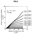
- FIG.8 is a graph showing a relation between drain-to-source voltage and drain-to-source current.
- the horizontal axis indicates voltage V DS between the source electrode 32 and the drain electrode 33 and the vertical axis indicates current I DS between the source electrode 32 and the drain electrode 33.
- Plural curved lines in the graph respectively shows values measured while changing voltage V GS between the gate electrode 31 and the source electrode 32 from +2 V to -24 V by -2 V.
- I DS decreases with decreasing V GS and it was conformed that the Ga 2 O 3 -based MESFET 30 operates normally.
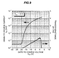
- FIG.9 is a graph showing a relation between gate-to-source voltage and drain-to-source current.
- the horizontal axis indicates voltage V GS between gate electrode 31 and the source electrode 32
- the vertical axis on the left side indicates current I DS between the drain electrode 33 and the source electrode 32
- the vertical axis on the right side indicates transconductance gm.
- a curved line on the left side in the graph shows I DS and that on the right side shows gm.
- Voltage V DS between the source electrode 32 and the drain electrode 33 was fixed to 40V.
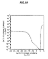
- FIG.10 is a graph showing a relation between gate-to-drain voltage and gate-to-drain current.
- the horizontal axis indicates voltage V GD between the gate electrode 31 and the drain electrode 33 and the vertical axis indicates gate leakage current I GD between the gate electrode 31 and the drain electrode 33.
- a high-quality Ga 2 O 3 -based semiconductor element is provided.
Landscapes
- Thin Film Transistor (AREA)
- Chemical & Material Sciences (AREA)
- Crystallography & Structural Chemistry (AREA)
- Physical Deposition Of Substances That Are Components Of Semiconductor Devices (AREA)
- Inorganic Chemistry (AREA)
- Junction Field-Effect Transistors (AREA)
Priority Applications (1)
| Application Number | Priority Date | Filing Date | Title |
|---|---|---|---|
| EP16198900.9A EP3151285B1 (de) | 2011-09-08 | 2012-09-07 | Ga2o3-basiertes halbleiterelement |
Applications Claiming Priority (2)
| Application Number | Priority Date | Filing Date | Title |
|---|---|---|---|
| JP2011196435 | 2011-09-08 | ||
| PCT/JP2012/072897 WO2013035842A1 (ja) | 2011-09-08 | 2012-09-07 | Ga2O3系半導体素子 |
Related Child Applications (2)
| Application Number | Title | Priority Date | Filing Date |
|---|---|---|---|
| EP16198900.9A Division EP3151285B1 (de) | 2011-09-08 | 2012-09-07 | Ga2o3-basiertes halbleiterelement |
| EP16198900.9A Division-Into EP3151285B1 (de) | 2011-09-08 | 2012-09-07 | Ga2o3-basiertes halbleiterelement |
Publications (3)
| Publication Number | Publication Date |
|---|---|
| EP2765612A1 true EP2765612A1 (de) | 2014-08-13 |
| EP2765612A4 EP2765612A4 (de) | 2015-07-22 |
| EP2765612B1 EP2765612B1 (de) | 2021-10-27 |
Family
ID=47832281
Family Applications (2)
| Application Number | Title | Priority Date | Filing Date |
|---|---|---|---|
| EP12829607.6A Active EP2765612B1 (de) | 2011-09-08 | 2012-09-07 | Ga2o3-halbleiterlement |
| EP16198900.9A Active EP3151285B1 (de) | 2011-09-08 | 2012-09-07 | Ga2o3-basiertes halbleiterelement |
Family Applications After (1)
| Application Number | Title | Priority Date | Filing Date |
|---|---|---|---|
| EP16198900.9A Active EP3151285B1 (de) | 2011-09-08 | 2012-09-07 | Ga2o3-basiertes halbleiterelement |
Country Status (5)
| Country | Link |
|---|---|
| US (2) | US9437689B2 (de) |
| EP (2) | EP2765612B1 (de) |
| JP (1) | JP5807282B2 (de) |
| CN (3) | CN103782392A (de) |
| WO (1) | WO2013035842A1 (de) |
Cited By (2)
| Publication number | Priority date | Publication date | Assignee | Title |
|---|---|---|---|---|
| EP2800128A4 (de) * | 2011-11-29 | 2015-02-25 | Tamura Seisakusho Kk | Verfahren zur herstellung eines ga2o3-kristallfilms |
| EP3151285A1 (de) | 2011-09-08 | 2017-04-05 | Tamura Corporation | Ga2o3-basiertes halbleiterelement |
Families Citing this family (58)
| Publication number | Priority date | Publication date | Assignee | Title |
|---|---|---|---|---|
| CN103782376B (zh) | 2011-09-08 | 2016-08-17 | 株式会社田村制作所 | Ga2O3系单晶体的供体浓度控制方法 |
| JP6284140B2 (ja) * | 2013-06-17 | 2018-02-28 | 株式会社タムラ製作所 | Ga2O3系半導体素子 |
| JP6543869B2 (ja) * | 2013-06-18 | 2019-07-17 | 株式会社タムラ製作所 | 半導体素子及びその製造方法 |
| JP6421446B2 (ja) * | 2013-06-28 | 2018-11-14 | 株式会社リコー | 電界効果型トランジスタ、表示素子、画像表示装置及びシステム |
| JP6662432B2 (ja) * | 2013-06-28 | 2020-03-11 | 株式会社リコー | 電界効果型トランジスタ、表示素子、画像表示装置及びシステム |
| JP6601738B2 (ja) * | 2013-09-30 | 2019-11-06 | 株式会社タムラ製作所 | 結晶積層構造体、及びその製造方法 |
| JP5984069B2 (ja) * | 2013-09-30 | 2016-09-06 | 株式会社タムラ製作所 | β−Ga2O3系単結晶膜の成長方法、及び結晶積層構造体 |
| EP2942804B1 (de) | 2014-05-08 | 2017-07-12 | Flosfia Inc. | Kristalline mehrschichtige Struktur und Halbleiterbauelement |
| JP6253150B2 (ja) * | 2014-05-09 | 2017-12-27 | 株式会社タムラ製作所 | エピタキシャルウエハ及びその製造方法 |
| JP5749839B1 (ja) * | 2014-06-30 | 2015-07-15 | 株式会社タムラ製作所 | β−Ga2O3系単結晶基板 |
| JP6344718B2 (ja) * | 2014-08-06 | 2018-06-20 | 株式会社タムラ製作所 | 結晶積層構造体及び半導体素子 |
| JP5907465B2 (ja) * | 2014-08-29 | 2016-04-26 | 株式会社タムラ製作所 | 半導体素子及び結晶積層構造体 |
| JP6406602B2 (ja) * | 2014-08-29 | 2018-10-17 | 株式会社タムラ製作所 | 半導体素子及びその製造方法、並びに結晶積層構造体 |
| JP5828568B1 (ja) * | 2014-08-29 | 2015-12-09 | 株式会社タムラ製作所 | 半導体素子及びその製造方法 |
| JP6376600B2 (ja) | 2015-03-20 | 2018-08-22 | 株式会社タムラ製作所 | 結晶積層構造体の製造方法 |
| JP6758569B2 (ja) * | 2015-03-20 | 2020-09-23 | 株式会社タムラ製作所 | 高耐圧ショットキーバリアダイオード |
| JP6845397B2 (ja) | 2016-04-28 | 2021-03-17 | 株式会社タムラ製作所 | トレンチmos型ショットキーダイオード |
| JP6844624B2 (ja) * | 2016-11-30 | 2021-03-17 | 株式会社リコー | 酸化物又は酸窒化物絶縁体膜形成用塗布液、酸化物又は酸窒化物絶縁体膜、電界効果型トランジスタ、及びそれらの製造方法 |
| CN106898644B (zh) * | 2017-01-23 | 2019-07-30 | 西安电子科技大学 | 高击穿电压场效应晶体管及其制作方法 |
| CN106876466B (zh) * | 2017-02-16 | 2020-11-13 | 大连理工大学 | 一种氧化镓基金属-氧化物半导体场效应晶体管及其制备方法 |
| JP7008293B2 (ja) | 2017-04-27 | 2022-01-25 | 国立研究開発法人情報通信研究機構 | Ga2O3系半導体素子 |
| CN107527949B (zh) * | 2017-06-07 | 2020-05-12 | 西安电子科技大学 | 基于Cr掺杂4H-SiC衬底异质结自旋场效应晶体管及其制备方法 |
| CN107425059B (zh) * | 2017-06-07 | 2020-05-22 | 西安电子科技大学 | Cr掺杂异质结自旋场效应晶体管及其制备方法 |
| CN107359127B (zh) * | 2017-06-07 | 2020-03-24 | 西安电子科技大学 | 蓝宝石衬底的Fe掺杂自旋场效应晶体管及其制造方法 |
| CN107369707B (zh) * | 2017-06-07 | 2020-03-24 | 西安电子科技大学 | 基于4H-SiC衬底异质结自旋场效应晶体管及其制造方法 |
| CN107658337B (zh) * | 2017-06-07 | 2020-09-08 | 西安电子科技大学 | 高电子迁移率自旋场效应晶体管及其制备方法 |
| CN107359122B (zh) * | 2017-06-07 | 2020-09-08 | 西安电子科技大学 | Mn掺杂异质结自旋场效应晶体管的制备方法 |
| JP7037142B2 (ja) * | 2017-08-10 | 2022-03-16 | 株式会社タムラ製作所 | ダイオード |
| JP7179276B2 (ja) * | 2017-09-29 | 2022-11-29 | 株式会社タムラ製作所 | 電界効果トランジスタ |
| JP7143601B2 (ja) * | 2018-03-16 | 2022-09-29 | 株式会社リコー | 電界効果型トランジスタ、表示素子、画像表示装置、及びシステム |
| WO2019191465A1 (en) * | 2018-03-28 | 2019-10-03 | Cornell University | VERTICAL GALLIUM OXIDE (Ga2O3) POWER FETS |
| TWI879736B (zh) * | 2018-07-12 | 2025-04-11 | 日商Flosfia股份有限公司 | 半導體裝置和半導體系統 |
| JP7404594B2 (ja) * | 2018-07-12 | 2023-12-26 | 株式会社Flosfia | 半導体装置および半導体装置を含む半導体システム |
| TWI897850B (zh) * | 2018-07-12 | 2025-09-21 | 日商Flosfia股份有限公司 | 半導體裝置和半導體系統 |
| TW202006945A (zh) * | 2018-07-12 | 2020-02-01 | 日商Flosfia股份有限公司 | 半導體裝置和半導體系統 |
| JP7162833B2 (ja) * | 2018-08-01 | 2022-10-31 | 国立研究開発法人物質・材料研究機構 | 半導体装置の製造方法 |
| US20200083332A1 (en) * | 2018-09-05 | 2020-03-12 | Industrial Technology Research Institute | Semiconductor device and method for fabricating the same |
| TWI700737B (zh) * | 2018-09-05 | 2020-08-01 | 財團法人工業技術研究院 | 半導體元件及其製造方法 |
| CN109537055A (zh) * | 2019-01-28 | 2019-03-29 | 山东大学 | 一种半绝缘氧化镓晶体及其制备方法 |
| CN109873038B (zh) * | 2019-03-19 | 2020-12-08 | 南方科技大学 | 一种场效应晶体管及其制备方法 |
| JP2020155530A (ja) * | 2019-03-19 | 2020-09-24 | トヨタ自動車株式会社 | 半導体装置の製造方法 |
| KR102741460B1 (ko) * | 2019-04-08 | 2024-12-12 | 에이지씨 가부시키가이샤 | 산화갈륨 기판, 및 산화갈륨 기판의 제조 방법 |
| JP7610270B2 (ja) * | 2019-06-06 | 2025-01-08 | ボーリング・グリーン・ステート・ユニバーシティ | 酸化物半導体の電気特性の調節方法並びに高電導性p型及びn型Ga2O3の開発 |
| CN110265486B (zh) * | 2019-06-20 | 2023-03-24 | 中国电子科技集团公司第十三研究所 | 氧化镓sbd终端结构及制备方法 |
| CN110571275A (zh) * | 2019-09-17 | 2019-12-13 | 中国科学技术大学 | 氧化镓mosfet的制备方法 |
| CN110993503B (zh) * | 2019-11-25 | 2023-02-24 | 韦华半导体(苏州)有限公司 | 基于氧化镓/钙钛矿传输层异质结的n型晶体管及其制备方法 |
| US11251268B2 (en) * | 2020-01-28 | 2022-02-15 | Taiwan Semiconductor Manufacturing Co., Ltd. | Semiconductor device with doped structure |
| JP6846754B2 (ja) * | 2020-03-31 | 2021-03-24 | 株式会社タムラ製作所 | 結晶積層構造体 |
| US11624126B2 (en) | 2020-06-16 | 2023-04-11 | Ohio State Innovation Foundation | Deposition of single phase beta-(AlxGa1-x)2O3 thin films with 0.28< =x<=0.7 on beta Ga2O3(100) or (−201) substrates by chemical vapor deposition |
| CN113517174B (zh) * | 2021-06-07 | 2023-08-08 | 西安电子科技大学 | 一种ε-Ga2O3薄膜的制备方法及ε-Ga2O3薄膜 |
| KR102516936B1 (ko) * | 2021-06-11 | 2023-03-31 | 숭실대학교산학협력단 | 향상모드 동작이 가능한 전계 효과 트랜지스터 소자 |
| CN113629148A (zh) * | 2021-06-24 | 2021-11-09 | 湖南大学 | 一种双栅极增强型氧化镓mesfet器件及其制作方法 |
| KR102641279B1 (ko) * | 2021-12-27 | 2024-02-27 | 재단법인차세대융합기술연구원 | 박막 전력 소자용 스태거드 금속-반도체 전계 효과 트랜지스터 |
| CN115976471A (zh) * | 2022-12-02 | 2023-04-18 | 中国科学院宁波材料技术与工程研究所 | Hf掺杂的氧化镓薄膜、其制备方法与应用 |
| EP4703501A1 (de) * | 2023-04-25 | 2026-03-04 | Mitsubishi Gas Chemical Company, Inc. | Verfahren zur herstellung eines schichtprodukts aus ss-ga2o3/?-ga2o3 und mit diesem herstellungsverfahren hergestelltes schichtprodukt |
| CN117012834A (zh) * | 2023-09-28 | 2023-11-07 | 深圳市港祥辉电子有限公司 | 一种高效散热氧化镓ldmosfet器件及其制备方法 |
| CN118621440B (zh) * | 2024-08-12 | 2024-11-22 | 深圳平湖实验室 | 一种半导体材料、半导体器件及制备方法 |
| CN118841449B (zh) * | 2024-09-20 | 2025-01-21 | 深圳市港祥辉电子有限公司 | 一种横向变掺杂沟道增强型氧化镓mos器件及其制备方法 |
Family Cites Families (40)
| Publication number | Priority date | Publication date | Assignee | Title |
|---|---|---|---|---|
| JPH07176640A (ja) | 1993-10-26 | 1995-07-14 | Fuji Electric Co Ltd | 半導体装置の製造方法 |
| JP3401918B2 (ja) * | 1994-07-04 | 2003-04-28 | 株式会社デンソー | 半導体装置 |
| JP3502531B2 (ja) | 1997-08-28 | 2004-03-02 | 株式会社ルネサステクノロジ | 半導体装置の製造方法 |
| US6686616B1 (en) * | 2000-05-10 | 2004-02-03 | Cree, Inc. | Silicon carbide metal-semiconductor field effect transistors |
| JP4083396B2 (ja) * | 2000-07-10 | 2008-04-30 | 独立行政法人科学技術振興機構 | 紫外透明導電膜とその製造方法 |
| US6844227B2 (en) * | 2000-12-26 | 2005-01-18 | Matsushita Electric Industrial Co., Ltd. | Semiconductor devices and method for manufacturing the same |
| US6916745B2 (en) | 2003-05-20 | 2005-07-12 | Fairchild Semiconductor Corporation | Structure and method for forming a trench MOSFET having self-aligned features |
| US6756320B2 (en) * | 2002-01-18 | 2004-06-29 | Freescale Semiconductor, Inc. | Method of forming article comprising an oxide layer on a GaAs-based semiconductor structure |
| JP3679097B2 (ja) * | 2002-05-31 | 2005-08-03 | 株式会社光波 | 発光素子 |
| US6940110B2 (en) * | 2002-11-29 | 2005-09-06 | Matsushita Electric Industrial Co., Ltd. | SiC-MISFET and method for fabricating the same |
| JP2004214607A (ja) * | 2002-12-19 | 2004-07-29 | Renesas Technology Corp | 半導体装置及びその製造方法 |
| KR100787272B1 (ko) * | 2003-02-24 | 2007-12-20 | 각코호진 와세다다이가쿠 | Ga2O3계 발광 소자 및 그 제조 방법 |
| JP4630986B2 (ja) * | 2003-02-24 | 2011-02-09 | 学校法人早稲田大学 | β−Ga2O3系単結晶成長方法 |
| US7638841B2 (en) | 2003-05-20 | 2009-12-29 | Fairchild Semiconductor Corporation | Power semiconductor devices and methods of manufacture |
| US7473929B2 (en) * | 2003-07-02 | 2009-01-06 | Panasonic Corporation | Semiconductor device and method for fabricating the same |
| TWI313060B (en) * | 2003-07-28 | 2009-08-01 | Japan Science & Tech Agency | Feild effect transisitor and fabricating method thereof |
| JP4066946B2 (ja) | 2003-12-18 | 2008-03-26 | 日産自動車株式会社 | 半導体装置 |
| JP2005235961A (ja) * | 2004-02-18 | 2005-09-02 | Univ Waseda | Ga2O3系単結晶の導電率制御方法 |
| JP4803634B2 (ja) * | 2004-10-01 | 2011-10-26 | 学校法人早稲田大学 | p型Ga2O3膜の製造方法およびpn接合型Ga2O3膜の製造方法 |
| US7265415B2 (en) | 2004-10-08 | 2007-09-04 | Fairchild Semiconductor Corporation | MOS-gated transistor with reduced miller capacitance |
| JP4956904B2 (ja) | 2005-03-25 | 2012-06-20 | 富士電機株式会社 | 炭化珪素半導体装置とその製造方法 |
| US7554137B2 (en) | 2005-10-25 | 2009-06-30 | Infineon Technologies Austria Ag | Power semiconductor component with charge compensation structure and method for the fabrication thereof |
| JP5145694B2 (ja) | 2006-11-07 | 2013-02-20 | 富士電機株式会社 | SiC半導体縦型MOSFETの製造方法。 |
| US7541260B2 (en) | 2007-02-21 | 2009-06-02 | Infineon Technologies Austria Ag | Trench diffusion isolation in semiconductor devices |
| JP2008303119A (ja) | 2007-06-08 | 2008-12-18 | Nippon Light Metal Co Ltd | 高機能性Ga2O3単結晶膜及びその製造方法 |
| JP5339698B2 (ja) * | 2007-08-20 | 2013-11-13 | 新日本無線株式会社 | 半導体装置の製造方法 |
| JP2009064970A (ja) | 2007-09-06 | 2009-03-26 | Toshiba Corp | 半導体装置 |
| JP2009070950A (ja) * | 2007-09-12 | 2009-04-02 | Koha Co Ltd | 紫外線センサ |
| JP2009111004A (ja) | 2007-10-26 | 2009-05-21 | Sumitomo Electric Ind Ltd | 絶縁ゲート型電界効果トランジスタおよびその製造方法 |
| JP5103683B2 (ja) | 2007-11-21 | 2012-12-19 | 日本軽金属株式会社 | 酸化ガリウム基板用電極の製造方法及びそれにより製造される酸化ガリウム基板用電極 |
| JP2009126764A (ja) | 2007-11-27 | 2009-06-11 | Nippon Light Metal Co Ltd | γ−Ga2O3の製造方法及びγ−Ga2O3 |
| JP5292968B2 (ja) | 2008-07-23 | 2013-09-18 | 住友電気工業株式会社 | 炭化珪素半導体装置の製造方法および炭化珪素半導体装置 |
| US20110233689A1 (en) * | 2008-12-08 | 2011-09-29 | Sumitomo Chemical Company, Limited | Semiconductor device, process for producing semiconductor device, semiconductor substrate, and process for producing semiconductor substrate |
| JP2010219130A (ja) | 2009-03-13 | 2010-09-30 | Sumitomo Electric Ind Ltd | 半導体装置およびその製造方法 |
| US8222107B2 (en) * | 2009-07-28 | 2012-07-17 | Panasonic Corporation | Method for producing semiconductor element |
| US8841682B2 (en) * | 2009-08-27 | 2014-09-23 | Cree, Inc. | Transistors with a gate insulation layer having a channel depleting interfacial charge and related fabrication methods |
| US8525257B2 (en) | 2009-11-18 | 2013-09-03 | Micrel, Inc. | LDMOS transistor with asymmetric spacer as gate |
| WO2012026209A1 (ja) * | 2010-08-25 | 2012-03-01 | シャープ株式会社 | 有機発光装置およびその帯電防止方法 |
| CN103782392A (zh) | 2011-09-08 | 2014-05-07 | 株式会社田村制作所 | Ga2O3 系半导体元件 |
| CN103782376B (zh) * | 2011-09-08 | 2016-08-17 | 株式会社田村制作所 | Ga2O3系单晶体的供体浓度控制方法 |
-
2012
- 2012-09-07 CN CN201280043332.7A patent/CN103782392A/zh active Pending
- 2012-09-07 EP EP12829607.6A patent/EP2765612B1/de active Active
- 2012-09-07 CN CN201910099983.1A patent/CN110010670A/zh active Pending
- 2012-09-07 US US14/343,367 patent/US9437689B2/en active Active
- 2012-09-07 WO PCT/JP2012/072897 patent/WO2013035842A1/ja not_active Ceased
- 2012-09-07 JP JP2013532670A patent/JP5807282B2/ja active Active
- 2012-09-07 CN CN201910099876.9A patent/CN110047922A/zh active Pending
- 2012-09-07 EP EP16198900.9A patent/EP3151285B1/de active Active
-
2016
- 2016-06-15 US US15/182,668 patent/US10249767B2/en active Active
Cited By (3)
| Publication number | Priority date | Publication date | Assignee | Title |
|---|---|---|---|---|
| EP3151285A1 (de) | 2011-09-08 | 2017-04-05 | Tamura Corporation | Ga2o3-basiertes halbleiterelement |
| EP2800128A4 (de) * | 2011-11-29 | 2015-02-25 | Tamura Seisakusho Kk | Verfahren zur herstellung eines ga2o3-kristallfilms |
| US9657410B2 (en) | 2011-11-29 | 2017-05-23 | Tamura Corporation | Method for producing Ga2O3 based crystal film |
Also Published As
| Publication number | Publication date |
|---|---|
| US20160300953A1 (en) | 2016-10-13 |
| US10249767B2 (en) | 2019-04-02 |
| EP2765612A4 (de) | 2015-07-22 |
| WO2013035842A1 (ja) | 2013-03-14 |
| EP3151285A1 (de) | 2017-04-05 |
| CN110010670A (zh) | 2019-07-12 |
| EP3151285B1 (de) | 2023-11-22 |
| EP2765612B1 (de) | 2021-10-27 |
| JPWO2013035842A1 (ja) | 2015-03-23 |
| JP5807282B2 (ja) | 2015-11-10 |
| US9437689B2 (en) | 2016-09-06 |
| CN103782392A (zh) | 2014-05-07 |
| US20140217469A1 (en) | 2014-08-07 |
| CN110047922A (zh) | 2019-07-23 |
Similar Documents
| Publication | Publication Date | Title |
|---|---|---|
| US10249767B2 (en) | Ga2O3-based semiconductor element | |
| US20180350967A1 (en) | Ga2O3 SEMICONDUCTOR ELEMENT | |
| US9716004B2 (en) | Crystal laminate structure and method for producing same | |
| US20140217470A1 (en) | Ga2O3 SEMICONDUCTOR ELEMENT | |
| EP2754738B1 (de) | Schottky-diode | |
| US20140217471A1 (en) | Ga2O3 SEMICONDUCTOR ELEMENT | |
| WO2013035841A1 (ja) | Ga2O3系HEMT | |
| Jo et al. | Effect of hydrogen in zinc oxide thin-film transistor grown by metal organic chemical vapor deposition |
Legal Events
| Date | Code | Title | Description |
|---|---|---|---|
| PUAI | Public reference made under article 153(3) epc to a published international application that has entered the european phase |
Free format text: ORIGINAL CODE: 0009012 |
|
| 17P | Request for examination filed |
Effective date: 20140310 |
|
| AK | Designated contracting states |
Kind code of ref document: A1 Designated state(s): AL AT BE BG CH CY CZ DE DK EE ES FI FR GB GR HR HU IE IS IT LI LT LU LV MC MK MT NL NO PL PT RO RS SE SI SK SM TR |
|
| DAX | Request for extension of the european patent (deleted) | ||
| RIC1 | Information provided on ipc code assigned before grant |
Ipc: H01L 21/336 20060101ALI20150226BHEP Ipc: H01L 29/26 20060101ALI20150226BHEP Ipc: H01L 21/02 20060101ALI20150226BHEP Ipc: H01L 29/786 20060101AFI20150226BHEP Ipc: H01L 29/812 20060101ALI20150226BHEP Ipc: H01L 29/78 20060101ALI20150226BHEP Ipc: H01L 29/24 20060101ALI20150226BHEP Ipc: H01L 21/20 20060101ALI20150226BHEP Ipc: H01L 29/772 20060101ALI20150226BHEP Ipc: H01L 21/338 20060101ALI20150226BHEP |
|
| RA4 | Supplementary search report drawn up and despatched (corrected) |
Effective date: 20150623 |
|
| RIC1 | Information provided on ipc code assigned before grant |
Ipc: H01L 29/24 20060101ALI20150617BHEP Ipc: H01L 21/336 20060101ALI20150617BHEP Ipc: H01L 21/02 20060101ALI20150617BHEP Ipc: H01L 29/78 20060101ALI20150617BHEP Ipc: H01L 21/338 20060101ALI20150617BHEP Ipc: H01L 29/786 20060101AFI20150617BHEP Ipc: H01L 21/20 20060101ALI20150617BHEP Ipc: H01L 29/772 20060101ALI20150617BHEP Ipc: H01L 29/26 20060101ALI20150617BHEP Ipc: H01L 29/812 20060101ALI20150617BHEP |
|
| 17Q | First examination report despatched |
Effective date: 20160705 |
|
| RAP1 | Party data changed (applicant data changed or rights of an application transferred) |
Owner name: TAMURA CORPORATION Owner name: NATIONAL INSTITUTE OF INFORMATION AND COMMUNICATIO |
|
| STAA | Information on the status of an ep patent application or granted ep patent |
Free format text: STATUS: EXAMINATION IS IN PROGRESS |
|
| GRAP | Despatch of communication of intention to grant a patent |
Free format text: ORIGINAL CODE: EPIDOSNIGR1 |
|
| STAA | Information on the status of an ep patent application or granted ep patent |
Free format text: STATUS: GRANT OF PATENT IS INTENDED |
|
| RIC1 | Information provided on ipc code assigned before grant |
Ipc: H01L 29/36 20060101ALI20210322BHEP Ipc: H01L 29/24 20060101ALI20210322BHEP Ipc: H01L 29/78 20060101ALI20210322BHEP Ipc: H01L 29/772 20060101ALI20210322BHEP Ipc: H01L 21/02 20060101ALI20210322BHEP Ipc: H01L 29/812 20060101ALI20210322BHEP Ipc: H01L 29/26 20060101ALI20210322BHEP Ipc: H01L 21/338 20060101ALI20210322BHEP Ipc: H01L 21/336 20060101ALI20210322BHEP Ipc: H01L 21/20 20060101ALI20210322BHEP Ipc: H01L 29/786 20060101AFI20210322BHEP |
|
| INTG | Intention to grant announced |
Effective date: 20210407 |
|
| GRAS | Grant fee paid |
Free format text: ORIGINAL CODE: EPIDOSNIGR3 |
|
| GRAA | (expected) grant |
Free format text: ORIGINAL CODE: 0009210 |
|
| STAA | Information on the status of an ep patent application or granted ep patent |
Free format text: STATUS: THE PATENT HAS BEEN GRANTED |
|
| AK | Designated contracting states |
Kind code of ref document: B1 Designated state(s): AL AT BE BG CH CY CZ DE DK EE ES FI FR GB GR HR HU IE IS IT LI LT LU LV MC MK MT NL NO PL PT RO RS SE SI SK SM TR |
|
| REG | Reference to a national code |
Ref country code: GB Ref legal event code: FG4D |
|
| REG | Reference to a national code |
Ref country code: CH Ref legal event code: EP |
|
| REG | Reference to a national code |
Ref country code: AT Ref legal event code: REF Ref document number: 1442620 Country of ref document: AT Kind code of ref document: T Effective date: 20211115 |
|
| REG | Reference to a national code |
Ref country code: DE Ref legal event code: R096 Ref document number: 602012077038 Country of ref document: DE |
|
| REG | Reference to a national code |
Ref country code: IE Ref legal event code: FG4D |
|
| REG | Reference to a national code |
Ref country code: LT Ref legal event code: MG9D |
|
| REG | Reference to a national code |
Ref country code: NL Ref legal event code: MP Effective date: 20211027 |
|
| REG | Reference to a national code |
Ref country code: AT Ref legal event code: MK05 Ref document number: 1442620 Country of ref document: AT Kind code of ref document: T Effective date: 20211027 |
|
| PG25 | Lapsed in a contracting state [announced via postgrant information from national office to epo] |
Ref country code: RS Free format text: LAPSE BECAUSE OF FAILURE TO SUBMIT A TRANSLATION OF THE DESCRIPTION OR TO PAY THE FEE WITHIN THE PRESCRIBED TIME-LIMIT Effective date: 20211027 Ref country code: LT Free format text: LAPSE BECAUSE OF FAILURE TO SUBMIT A TRANSLATION OF THE DESCRIPTION OR TO PAY THE FEE WITHIN THE PRESCRIBED TIME-LIMIT Effective date: 20211027 Ref country code: FI Free format text: LAPSE BECAUSE OF FAILURE TO SUBMIT A TRANSLATION OF THE DESCRIPTION OR TO PAY THE FEE WITHIN THE PRESCRIBED TIME-LIMIT Effective date: 20211027 Ref country code: BG Free format text: LAPSE BECAUSE OF FAILURE TO SUBMIT A TRANSLATION OF THE DESCRIPTION OR TO PAY THE FEE WITHIN THE PRESCRIBED TIME-LIMIT Effective date: 20220127 Ref country code: AT Free format text: LAPSE BECAUSE OF FAILURE TO SUBMIT A TRANSLATION OF THE DESCRIPTION OR TO PAY THE FEE WITHIN THE PRESCRIBED TIME-LIMIT Effective date: 20211027 |
|
| PG25 | Lapsed in a contracting state [announced via postgrant information from national office to epo] |
Ref country code: IS Free format text: LAPSE BECAUSE OF FAILURE TO SUBMIT A TRANSLATION OF THE DESCRIPTION OR TO PAY THE FEE WITHIN THE PRESCRIBED TIME-LIMIT Effective date: 20220227 Ref country code: SE Free format text: LAPSE BECAUSE OF FAILURE TO SUBMIT A TRANSLATION OF THE DESCRIPTION OR TO PAY THE FEE WITHIN THE PRESCRIBED TIME-LIMIT Effective date: 20211027 Ref country code: PT Free format text: LAPSE BECAUSE OF FAILURE TO SUBMIT A TRANSLATION OF THE DESCRIPTION OR TO PAY THE FEE WITHIN THE PRESCRIBED TIME-LIMIT Effective date: 20220228 Ref country code: PL Free format text: LAPSE BECAUSE OF FAILURE TO SUBMIT A TRANSLATION OF THE DESCRIPTION OR TO PAY THE FEE WITHIN THE PRESCRIBED TIME-LIMIT Effective date: 20211027 Ref country code: NO Free format text: LAPSE BECAUSE OF FAILURE TO SUBMIT A TRANSLATION OF THE DESCRIPTION OR TO PAY THE FEE WITHIN THE PRESCRIBED TIME-LIMIT Effective date: 20220127 Ref country code: NL Free format text: LAPSE BECAUSE OF FAILURE TO SUBMIT A TRANSLATION OF THE DESCRIPTION OR TO PAY THE FEE WITHIN THE PRESCRIBED TIME-LIMIT Effective date: 20211027 Ref country code: LV Free format text: LAPSE BECAUSE OF FAILURE TO SUBMIT A TRANSLATION OF THE DESCRIPTION OR TO PAY THE FEE WITHIN THE PRESCRIBED TIME-LIMIT Effective date: 20211027 Ref country code: HR Free format text: LAPSE BECAUSE OF FAILURE TO SUBMIT A TRANSLATION OF THE DESCRIPTION OR TO PAY THE FEE WITHIN THE PRESCRIBED TIME-LIMIT Effective date: 20211027 Ref country code: GR Free format text: LAPSE BECAUSE OF FAILURE TO SUBMIT A TRANSLATION OF THE DESCRIPTION OR TO PAY THE FEE WITHIN THE PRESCRIBED TIME-LIMIT Effective date: 20220128 Ref country code: ES Free format text: LAPSE BECAUSE OF FAILURE TO SUBMIT A TRANSLATION OF THE DESCRIPTION OR TO PAY THE FEE WITHIN THE PRESCRIBED TIME-LIMIT Effective date: 20211027 |
|
| REG | Reference to a national code |
Ref country code: DE Ref legal event code: R097 Ref document number: 602012077038 Country of ref document: DE |
|
| PG25 | Lapsed in a contracting state [announced via postgrant information from national office to epo] |
Ref country code: SM Free format text: LAPSE BECAUSE OF FAILURE TO SUBMIT A TRANSLATION OF THE DESCRIPTION OR TO PAY THE FEE WITHIN THE PRESCRIBED TIME-LIMIT Effective date: 20211027 Ref country code: SK Free format text: LAPSE BECAUSE OF FAILURE TO SUBMIT A TRANSLATION OF THE DESCRIPTION OR TO PAY THE FEE WITHIN THE PRESCRIBED TIME-LIMIT Effective date: 20211027 Ref country code: RO Free format text: LAPSE BECAUSE OF FAILURE TO SUBMIT A TRANSLATION OF THE DESCRIPTION OR TO PAY THE FEE WITHIN THE PRESCRIBED TIME-LIMIT Effective date: 20211027 Ref country code: EE Free format text: LAPSE BECAUSE OF FAILURE TO SUBMIT A TRANSLATION OF THE DESCRIPTION OR TO PAY THE FEE WITHIN THE PRESCRIBED TIME-LIMIT Effective date: 20211027 Ref country code: DK Free format text: LAPSE BECAUSE OF FAILURE TO SUBMIT A TRANSLATION OF THE DESCRIPTION OR TO PAY THE FEE WITHIN THE PRESCRIBED TIME-LIMIT Effective date: 20211027 Ref country code: CZ Free format text: LAPSE BECAUSE OF FAILURE TO SUBMIT A TRANSLATION OF THE DESCRIPTION OR TO PAY THE FEE WITHIN THE PRESCRIBED TIME-LIMIT Effective date: 20211027 |
|
| PLBE | No opposition filed within time limit |
Free format text: ORIGINAL CODE: 0009261 |
|
| STAA | Information on the status of an ep patent application or granted ep patent |
Free format text: STATUS: NO OPPOSITION FILED WITHIN TIME LIMIT |
|
| 26N | No opposition filed |
Effective date: 20220728 |
|
| PG25 | Lapsed in a contracting state [announced via postgrant information from national office to epo] |
Ref country code: AL Free format text: LAPSE BECAUSE OF FAILURE TO SUBMIT A TRANSLATION OF THE DESCRIPTION OR TO PAY THE FEE WITHIN THE PRESCRIBED TIME-LIMIT Effective date: 20211027 |
|
| PG25 | Lapsed in a contracting state [announced via postgrant information from national office to epo] |
Ref country code: SI Free format text: LAPSE BECAUSE OF FAILURE TO SUBMIT A TRANSLATION OF THE DESCRIPTION OR TO PAY THE FEE WITHIN THE PRESCRIBED TIME-LIMIT Effective date: 20211027 |
|
| PG25 | Lapsed in a contracting state [announced via postgrant information from national office to epo] |
Ref country code: MC Free format text: LAPSE BECAUSE OF FAILURE TO SUBMIT A TRANSLATION OF THE DESCRIPTION OR TO PAY THE FEE WITHIN THE PRESCRIBED TIME-LIMIT Effective date: 20211027 |
|
| REG | Reference to a national code |
Ref country code: CH Ref legal event code: PL |
|
| GBPC | Gb: european patent ceased through non-payment of renewal fee |
Effective date: 20220907 |
|
| REG | Reference to a national code |
Ref country code: BE Ref legal event code: MM Effective date: 20220930 |
|
| PG25 | Lapsed in a contracting state [announced via postgrant information from national office to epo] |
Ref country code: IT Free format text: LAPSE BECAUSE OF FAILURE TO SUBMIT A TRANSLATION OF THE DESCRIPTION OR TO PAY THE FEE WITHIN THE PRESCRIBED TIME-LIMIT Effective date: 20211027 |
|
| PG25 | Lapsed in a contracting state [announced via postgrant information from national office to epo] |
Ref country code: LU Free format text: LAPSE BECAUSE OF NON-PAYMENT OF DUE FEES Effective date: 20220907 |
|
| PG25 | Lapsed in a contracting state [announced via postgrant information from national office to epo] |
Ref country code: LI Free format text: LAPSE BECAUSE OF NON-PAYMENT OF DUE FEES Effective date: 20220930 Ref country code: IE Free format text: LAPSE BECAUSE OF NON-PAYMENT OF DUE FEES Effective date: 20220907 Ref country code: FR Free format text: LAPSE BECAUSE OF NON-PAYMENT OF DUE FEES Effective date: 20220930 Ref country code: CH Free format text: LAPSE BECAUSE OF NON-PAYMENT OF DUE FEES Effective date: 20220930 |
|
| PG25 | Lapsed in a contracting state [announced via postgrant information from national office to epo] |
Ref country code: BE Free format text: LAPSE BECAUSE OF NON-PAYMENT OF DUE FEES Effective date: 20220930 |
|
| PG25 | Lapsed in a contracting state [announced via postgrant information from national office to epo] |
Ref country code: GB Free format text: LAPSE BECAUSE OF NON-PAYMENT OF DUE FEES Effective date: 20220907 |
|
| PG25 | Lapsed in a contracting state [announced via postgrant information from national office to epo] |
Ref country code: HU Free format text: LAPSE BECAUSE OF FAILURE TO SUBMIT A TRANSLATION OF THE DESCRIPTION OR TO PAY THE FEE WITHIN THE PRESCRIBED TIME-LIMIT; INVALID AB INITIO Effective date: 20120907 |
|
| PG25 | Lapsed in a contracting state [announced via postgrant information from national office to epo] |
Ref country code: CY Free format text: LAPSE BECAUSE OF FAILURE TO SUBMIT A TRANSLATION OF THE DESCRIPTION OR TO PAY THE FEE WITHIN THE PRESCRIBED TIME-LIMIT Effective date: 20211027 |
|
| PG25 | Lapsed in a contracting state [announced via postgrant information from national office to epo] |
Ref country code: MK Free format text: LAPSE BECAUSE OF FAILURE TO SUBMIT A TRANSLATION OF THE DESCRIPTION OR TO PAY THE FEE WITHIN THE PRESCRIBED TIME-LIMIT Effective date: 20211027 |
|
| PG25 | Lapsed in a contracting state [announced via postgrant information from national office to epo] |
Ref country code: TR Free format text: LAPSE BECAUSE OF FAILURE TO SUBMIT A TRANSLATION OF THE DESCRIPTION OR TO PAY THE FEE WITHIN THE PRESCRIBED TIME-LIMIT Effective date: 20211027 |
|
| PG25 | Lapsed in a contracting state [announced via postgrant information from national office to epo] |
Ref country code: MT Free format text: LAPSE BECAUSE OF FAILURE TO SUBMIT A TRANSLATION OF THE DESCRIPTION OR TO PAY THE FEE WITHIN THE PRESCRIBED TIME-LIMIT Effective date: 20211027 |
|
| REG | Reference to a national code |
Ref country code: DE Ref legal event code: R079 Ref document number: 602012077038 Country of ref document: DE Free format text: PREVIOUS MAIN CLASS: H01L0029786000 Ipc: H10D0030670000 |
|
| PGFP | Annual fee paid to national office [announced via postgrant information from national office to epo] |
Ref country code: DE Payment date: 20250919 Year of fee payment: 14 |