EP2765617A2 - Procédé de fabrication de barreaux de silicium, en particulier de barreaux de silicium pour cellules solaires, et dispositif de fabrication de barreaux de silicium - Google Patents
Procédé de fabrication de barreaux de silicium, en particulier de barreaux de silicium pour cellules solaires, et dispositif de fabrication de barreaux de silicium Download PDFInfo
- Publication number
- EP2765617A2 EP2765617A2 EP14151363.0A EP14151363A EP2765617A2 EP 2765617 A2 EP2765617 A2 EP 2765617A2 EP 14151363 A EP14151363 A EP 14151363A EP 2765617 A2 EP2765617 A2 EP 2765617A2
- Authority
- EP
- European Patent Office
- Prior art keywords
- wafer
- wafers
- base body
- wafer base
- carrier element
- Prior art date
- Legal status (The legal status is an assumption and is not a legal conclusion. Google has not performed a legal analysis and makes no representation as to the accuracy of the status listed.)
- Withdrawn
Links
- 238000004519 manufacturing process Methods 0.000 title claims abstract description 10
- 235000012431 wafers Nutrition 0.000 title claims description 153
- 238000000034 method Methods 0.000 claims abstract description 23
- 230000015572 biosynthetic process Effects 0.000 claims abstract description 3
- 238000000926 separation method Methods 0.000 claims description 10
- 238000005516 engineering process Methods 0.000 claims description 7
- 239000006181 electrochemical material Substances 0.000 claims description 2
- XUIMIQQOPSSXEZ-UHFFFAOYSA-N Silicon Chemical compound [Si] XUIMIQQOPSSXEZ-UHFFFAOYSA-N 0.000 description 4
- 239000000853 adhesive Substances 0.000 description 4
- 230000001070 adhesive effect Effects 0.000 description 4
- 229910052710 silicon Inorganic materials 0.000 description 4
- 239000010703 silicon Substances 0.000 description 4
- 239000012790 adhesive layer Substances 0.000 description 2
- 210000000078 claw Anatomy 0.000 description 2
- 239000007788 liquid Substances 0.000 description 2
- 239000000126 substance Substances 0.000 description 2
- 241000252254 Catostomidae Species 0.000 description 1
- 239000002253 acid Substances 0.000 description 1
- 238000011161 development Methods 0.000 description 1
- 230000018109 developmental process Effects 0.000 description 1
- 239000003792 electrolyte Substances 0.000 description 1
- 239000011521 glass Substances 0.000 description 1
- 239000010410 layer Substances 0.000 description 1
- 238000011089 mechanical engineering Methods 0.000 description 1
- 230000007704 transition Effects 0.000 description 1
- XLYOFNOQVPJJNP-UHFFFAOYSA-N water Substances O XLYOFNOQVPJJNP-UHFFFAOYSA-N 0.000 description 1
Images

Classifications
-
- H—ELECTRICITY
- H10—SEMICONDUCTOR DEVICES; ELECTRIC SOLID-STATE DEVICES NOT OTHERWISE PROVIDED FOR
- H10F—INORGANIC SEMICONDUCTOR DEVICES SENSITIVE TO INFRARED RADIATION, LIGHT, ELECTROMAGNETIC RADIATION OF SHORTER WAVELENGTH OR CORPUSCULAR RADIATION
- H10F71/00—Manufacture or treatment of devices covered by this subclass
- H10F71/121—The active layers comprising only Group IV materials
- H10F71/1221—The active layers comprising only Group IV materials comprising polycrystalline silicon
-
- B—PERFORMING OPERATIONS; TRANSPORTING
- B28—WORKING CEMENT, CLAY, OR STONE
- B28D—WORKING STONE OR STONE-LIKE MATERIALS
- B28D5/00—Fine working of gems, jewels, crystals, e.g. of semiconductor material; apparatus or devices therefor
- B28D5/0058—Accessories specially adapted for use with machines for fine working of gems, jewels, crystals, e.g. of semiconductor material
- B28D5/0082—Accessories specially adapted for use with machines for fine working of gems, jewels, crystals, e.g. of semiconductor material for supporting, holding, feeding, conveying or discharging work
- B28D5/0094—Accessories specially adapted for use with machines for fine working of gems, jewels, crystals, e.g. of semiconductor material for supporting, holding, feeding, conveying or discharging work the supporting or holding device being of the vacuum type
-
- B—PERFORMING OPERATIONS; TRANSPORTING
- B28—WORKING CEMENT, CLAY, OR STONE
- B28D—WORKING STONE OR STONE-LIKE MATERIALS
- B28D5/00—Fine working of gems, jewels, crystals, e.g. of semiconductor material; apparatus or devices therefor
- B28D5/04—Fine working of gems, jewels, crystals, e.g. of semiconductor material; apparatus or devices therefor by tools other than rotary type, e.g. reciprocating tools
- B28D5/045—Fine working of gems, jewels, crystals, e.g. of semiconductor material; apparatus or devices therefor by tools other than rotary type, e.g. reciprocating tools by cutting with wires or closed-loop blades
-
- Y—GENERAL TAGGING OF NEW TECHNOLOGICAL DEVELOPMENTS; GENERAL TAGGING OF CROSS-SECTIONAL TECHNOLOGIES SPANNING OVER SEVERAL SECTIONS OF THE IPC; TECHNICAL SUBJECTS COVERED BY FORMER USPC CROSS-REFERENCE ART COLLECTIONS [XRACs] AND DIGESTS
- Y02—TECHNOLOGIES OR APPLICATIONS FOR MITIGATION OR ADAPTATION AGAINST CLIMATE CHANGE
- Y02E—REDUCTION OF GREENHOUSE GAS [GHG] EMISSIONS, RELATED TO ENERGY GENERATION, TRANSMISSION OR DISTRIBUTION
- Y02E10/00—Energy generation through renewable energy sources
- Y02E10/50—Photovoltaic [PV] energy
- Y02E10/546—Polycrystalline silicon PV cells
-
- Y—GENERAL TAGGING OF NEW TECHNOLOGICAL DEVELOPMENTS; GENERAL TAGGING OF CROSS-SECTIONAL TECHNOLOGIES SPANNING OVER SEVERAL SECTIONS OF THE IPC; TECHNICAL SUBJECTS COVERED BY FORMER USPC CROSS-REFERENCE ART COLLECTIONS [XRACs] AND DIGESTS
- Y02—TECHNOLOGIES OR APPLICATIONS FOR MITIGATION OR ADAPTATION AGAINST CLIMATE CHANGE
- Y02P—CLIMATE CHANGE MITIGATION TECHNOLOGIES IN THE PRODUCTION OR PROCESSING OF GOODS
- Y02P70/00—Climate change mitigation technologies in the production process for final industrial or consumer products
- Y02P70/50—Manufacturing or production processes characterised by the final manufactured product
Definitions
- the invention relates to a method for producing wafers, in particular wafers for solar cells, according to the preamble of claim 1. Furthermore, the invention relates to a device for producing wafers.
- a method according to the preamble of claim 1 is already well known in the art, and is used in the production of wafers for solar cells.
- a prefabricated, consisting of silicon block-shaped wafer body is attached to the interposition of a particular existing glass loss or sacrificial plate on a support plate formed as a tool element.
- the tool plate can in turn be attached to the tool table of a processing machine.
- the attachment between the wafer base body, the sacrificial plate and the tool plate via two adhesive layers, which are arranged on both sides of the sacrificial plate on the wafer base body or the tool plate side facing.
- a wafer base body fastened to a tool plate in this way is then subdivided or sawed off from the side facing away from the tool plate into disk-shaped wafers, the separator sawing the wafer body over its entire height and the cuts of the wire saw into the sacrificial plate be executed in it.
- the separated by the separator, and still associated by the sacrificial plate wafer from the wafer base or the sacrificial plate are separated by the wafer body is placed together with the sacrificial plate in a bath with hot water or dilute acid. It is important that the adhesive does not contaminate the release bath and the silicon, but sticks to the loss plate.
- a disadvantage of the known from the prior art It is a method that the handling for separating the individual wafers from the wafer base body by the necessity of the bath with the substances contained therein is relatively complex.
- positional inaccuracies in the (vertical) positioning of the wafer base body to the tool plate can occur through the attachment of the wafer base body via the two adhesive layers, which are arranged on both sides of the sacrificial plate, in a non-angular or non-perpendicular arrangement of the wafer base body lead to the tool plate.
- inaccuracies in the geometry of the individual wafers are produced when the wafers are separated from the wafer base body, which leads either to an increased scrap or, if this makes economic sense, possibly to undesired reworking.
- the present invention seeks to provide a method for producing wafers, in particular of wafers for solar cells, according to the preamble of claim 1 such that a simplified handling at the same time allows particularly good positioning accuracy of the wafer body to the support element becomes.
- This object is achieved in a method for producing wafers with the features of claim 1, characterized in that the wafer body is by means of an adhesive-free connection technology force and / or positively secured to the support member.
- the carrier element is understood to be any element which is suitable for fastening the wafer base body to a suitable machine tool for forming the wafer.
- the term carrier element should therefore by no means be limited to plate-shaped elements.
- the adhesive-free connection technique in the form of a mechanically or pneumatically acting clamping device or a clamping element, in particular in the form of a screw is formed, which is or is arranged directly in operative connection with the wafer body.
- the tensioning device or the tensioning element cooperate with at least one surface or recess formed in the wafer base body.
- a recess may be formed, for example in the form of a nutsteinförmigen recess, a threaded bore, a slot or the like, into which a shape of the recess adapted retaining element of the clamping device engages, which in turn is connected to the carrier element.
- the wafer base body has a useful region which serves to form the disk-shaped wafers, and in that a holding region of the wafer main body adjoins the useful region on the side facing the carrier element.
- the recesses for the positive and / or non-positive connection of the wafer base body formed on the support member, or the holding portion includes, for example, a plane contact surface for a pneumatically acting vacuum cleaner, secured by the wafer body to the support element is.
- the size of the holding region can be designed in such a way that, compared with the prior art for producing a certain number and / or size of wafers, no enlarged wafer base body is required.
- the separating device is moved as far as the region of the holding region of the wafer body during the formation of the wafer.
- the maximum possible height of the wafer base body is utilized to produce the wafers.
- a particularly simple or economical separation process of the wafers from the wafer base body is achieved if the separation of the wafers from the wafer base body is effected by a separation process which comprises cutting the wafer base body in the region of the end faces of the wafers in a direction perpendicular to the wafers.
- the separation takes place through the separating device, which also serves to form the wafers from the wafer base body.
- the separating device which also serves to form the wafers from the wafer base body.
- the singulation takes place by means of a separating device that is different from the separating device for forming the wafers from the wafer main body.
- a separating device that is different from the separating device for forming the wafers from the wafer main body.
- Such a procedure makes it possible to use optimized separating devices for the respective operation (forming disk-shaped wafers from the wafer base body and for perpendicularly separating the wafers from the wafer base body), which for example enable particularly high surface qualities at the respective cutting edges or particularly effective, ie. make fast cuts possible.
- the wafer base body is arranged in an electrolyte liquid, wherein the wafer base body is connected to one pole of a voltage source, and the singulator (for example in the form of wires) is connected to the other pole of the voltage source.
- the invention also includes an apparatus for producing wafers (100), in particular for carrying out the method according to the invention, wherein a carrier element is provided on which a wafer base body can be fastened.
- a mechanically or pneumatically acting clamping device or a clamping element is arranged on the carrier element.
- Such a clamping device may for example be in the form of known from mechanical engineering clamping claws or the like or in the form of one or more suckers.
- a tensioning element can, for example, be used as a fastening screw or the like. be educated.
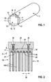
- a cast block 1 made of silicon is shown in the form of a cylinder having a round cross-section.
- the cross section of a block-shaped Wafer body 10 recognizable, which has a substantially rectangular cross-section with four straight side surfaces 11 and rounded or bevelled corners 12.
- the cross-section of the wafer base body 10 described so far forms a useful area 15 which is used to form disc-shaped wafers 100, which serve in particular for the production of solar cells.
- a holding area 16 adjoins with a height h, wherein the flat boundary surface 17 facing away from the side surface 11, which runs parallel to the side surface 11, as an attachment surface to a in the Fig. 2 recognizable support member in the form of a tool plate 20 is used.
- the wafer basic body 10, consisting of the useful area 15 and the holding area 16, is formed in particular by a device designed as a saw from the cast block 1 (not shown).
- the wafer base body 10 described so far is fixed with the flat boundary surface 17 against the likewise flat contact surface 21 of the tool plate 20.
- the state is shown which sets in at the end of a processing of the wafer base body 10, in which a separator 25 in the form of a wire saw with a plurality of mutually parallel individual wires 26 of the tool plate 20 remote from the wafer body 10 perpendicular to the plane of the tool plate 20 and the contact surface 21 has performed leading saw cuts, so that a plurality of mutually parallel wafers 100 in the wafer body 10, in particular in the effective area 15 of the wafer body 10, are formed.
- the boundary line 27 is in the Fig. 2 the transition from the useful area 15 into the holding area 16 of the wafer body 10 is characterized. It can be seen that the individual wires 26 of the separating device 25 have been guided into the holding region 15. The separation of the individual wafers 100 from the wafer body 10 is then carried out by a relative movement between the separator 25 and the individual wires 26 and the wafer body 10 in a plane parallel to the contact surface 21 of the tool plate 20 corresponding to the direction of the double arrow 28. The dividing plane forms the a side surfaces of the wafer 100 from. According to the invention, it is provided that the attachment of the wafer body 10 via the holding portion 16 to the contact surface 21 of the tool plate 20 by means of an adhesive-free connection technology. Such a connection technique is formed in the context of the invention as a positive and / or non-positive connection technology.
- a first embodiment of this connection technique is based on the Fig. 2 and 3 shown, it is seen that in the holding portion 16 of the wafer body 10 a plurality of mutually parallel recesses in the form of threaded holes 29 are provided which extend perpendicular to the boundary surface 17 and the contact surface 21 of the tool plate 20.
- the wafer body 10 can thus be clamped and positioned with its boundary surface 17 directly against the contact surface 21 of the support member or the tool plate 20 ,
- Fig. 4 is the holding portion 16 in the form of a over the entire length of the wafer body 10 extending holding web 31 is formed, in which, for example, a plurality of perpendicular to the plane of the Fig. 4 trained threaded holes 29 are formed.
- the holding web 31 has two oppositely disposed side surfaces 32, 33, which can be used, for example, to be arranged in operative connection with a corresponding groove-shaped receptacle of the tool plate 20 in order to position the wafer body 10 to the tool plate 20 or to its contact surface 21.
- Fig. 5 is one opposite the Fig. 4 modified embodiment of the invention shown, in which the holding web 31a extends laterally to the (round) basic cross section of the ingot 1.
- the holding web 31a extends laterally to the (round) basic cross section of the ingot 1.
- 33a threaded bores 29 are formed, which extend parallel to the boundary surface 17a of the wafer body 10.
- a further embodiment of the invention is shown, in which in the boundary surface 17b of the wafer body 10 and the holding portion 16 of the wafer body 10 four, each having an undercut 34 having recesses 35 are formed.
- the wafer body 10 can be positively or non-positively attached to the contact surface 21 of the tool plate 20 via corresponding counter-elements.
- FIG. 7 and 8th modified holding regions 16 of a wafer body 10 are shown.
- the retaining region 16 on opposite side surfaces 36, 37 each have a rectangular cross-section having retaining grooves 38, via which the wafer body 10, for example by means of holding claws on the tool plate 20 and the contact surface 21 can be directly attached.
- an undercut 39 having mounting groove 40 is provided, can be attached to the tool plate 20 via the corresponding base blocks 10 of the wafer base body.
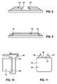
- FIGS. 9 and 10 an embodiment of the invention is shown, in which the wafer base body 10 on opposite side surfaces 41, 42 of the holding portion 16 by means of a in the Fig. 10 illustrated, in cross-section L-shaped bracket 43, 44 having clamping device 45 can be attached to the tool plate 20.
- Last is in the Fig. 11 an embodiment of the invention shown, in which the planar boundary surface 17 of the holding portion 16 serves as an abutment for two pneumatically operated suction cups 46, 47, which in turn can be fastened to the tool plate 20 and contact surface 21.
- the tool plate 20 as a carrier element together with the mechanically or pneumatically acting clamping device 45, 46, 47 or the clamping element 30 part of a device for producing wafers 100th
- the method described so far for attaching a wafer base body 10 to a carrier element designed in particular as a tool plate 20 can be modified or modified in a variety of ways, without deviating from the idea of the invention.
- the only important thing is that the Connection or attachment of the wafer body 10 via a positive and / or non-positive connection technology takes place in which the use of adhesives is not required.
Landscapes
- Engineering & Computer Science (AREA)
- Mechanical Engineering (AREA)
- Container, Conveyance, Adherence, Positioning, Of Wafer (AREA)
- Mechanical Treatment Of Semiconductor (AREA)
- Processing Of Stones Or Stones Resemblance Materials (AREA)
Applications Claiming Priority (1)
| Application Number | Priority Date | Filing Date | Title |
|---|---|---|---|
| DE102013202028.7A DE102013202028A1 (de) | 2013-02-07 | 2013-02-07 | Verfahren zum Herstellen von Wafern, insbesondere von Wafern für Solarzellen, und Vorrichtung zum Herstellen von Wafern |
Publications (2)
| Publication Number | Publication Date |
|---|---|
| EP2765617A2 true EP2765617A2 (fr) | 2014-08-13 |
| EP2765617A3 EP2765617A3 (fr) | 2017-08-30 |
Family
ID=49955943
Family Applications (1)
| Application Number | Title | Priority Date | Filing Date |
|---|---|---|---|
| EP14151363.0A Withdrawn EP2765617A3 (fr) | 2013-02-07 | 2014-01-16 | Procédé de fabrication de barreaux de silicium, en particulier de barreaux de silicium pour cellules solaires, et dispositif de fabrication de barreaux de silicium |
Country Status (2)
| Country | Link |
|---|---|
| EP (1) | EP2765617A3 (fr) |
| DE (1) | DE102013202028A1 (fr) |
Cited By (2)
| Publication number | Priority date | Publication date | Assignee | Title |
|---|---|---|---|---|
| CN114454359A (zh) * | 2021-07-13 | 2022-05-10 | 青岛高测科技股份有限公司 | 硅棒切割方法、设备及系统 |
| CN114454360A (zh) * | 2021-08-19 | 2022-05-10 | 青岛高测科技股份有限公司 | 硅棒切割方法、设备及系统 |
Family Cites Families (4)
| Publication number | Priority date | Publication date | Assignee | Title |
|---|---|---|---|---|
| JP2551229B2 (ja) * | 1990-11-01 | 1996-11-06 | 住友金属工業株式会社 | マルチワイヤソーによる切断方法およびその装置 |
| DE69526038T2 (de) * | 1994-12-15 | 2002-10-31 | Sharp K.K., Osaka | Drahtgittersäge und Sägeverfahren |
| DE102005014052A1 (de) * | 2004-03-24 | 2005-10-13 | Itb Gmbh | Verfahren und Vorrichtung zum Schneiden eines Blocks in dünne Scheiben mittels Drahtsägen |
| US20130251940A1 (en) * | 2012-03-23 | 2013-09-26 | Sheng Sun | Method of cutting an ingot for solar cell fabrication |
-
2013
- 2013-02-07 DE DE102013202028.7A patent/DE102013202028A1/de not_active Withdrawn
-
2014
- 2014-01-16 EP EP14151363.0A patent/EP2765617A3/fr not_active Withdrawn
Non-Patent Citations (1)
| Title |
|---|
| None |
Cited By (4)
| Publication number | Priority date | Publication date | Assignee | Title |
|---|---|---|---|---|
| CN114454359A (zh) * | 2021-07-13 | 2022-05-10 | 青岛高测科技股份有限公司 | 硅棒切割方法、设备及系统 |
| CN114454362A (zh) * | 2021-07-13 | 2022-05-10 | 青岛高测科技股份有限公司 | 硅棒切割方法、设备及系统 |
| CN114454359B (zh) * | 2021-07-13 | 2024-05-14 | 青岛高测科技股份有限公司 | 硅棒切割方法、设备及系统 |
| CN114454360A (zh) * | 2021-08-19 | 2022-05-10 | 青岛高测科技股份有限公司 | 硅棒切割方法、设备及系统 |
Also Published As
| Publication number | Publication date |
|---|---|
| EP2765617A3 (fr) | 2017-08-30 |
| DE102013202028A1 (de) | 2014-08-07 |
Similar Documents
| Publication | Publication Date | Title |
|---|---|---|
| DE68909316T2 (de) | Vorrichtung zum automatischen Trennen entlang vorherbestimmter Biegebruchlinien in keramischen Grundplättchen von elektronischen Hybridschaltungen. | |
| EP1332247B1 (fr) | Procede et dispositif pour le decoupage de monocristaux, dispositif d'ajustage et procede de test pour determiner une orientation cristalline | |
| DE102005028112A1 (de) | Verfahren zur Positionierung und Lageerhaltung von Substraten, insbesondere von dünnen Siliziumwafern nach dem Drahtsägen zu deren Vereinzelung | |
| EP1240529A2 (fr) | Procede de fabrication de structures micro-mecaniques | |
| DE102010050897B4 (de) | Trägervorrichtung und Verfahren zum Schneiden eines an der Trägervorrichtung befestigten Materialblocks | |
| EP2990172A1 (fr) | Procédé de séparation d'objets en forme de plaque en matériaux cassants | |
| EP2765617A2 (fr) | Procédé de fabrication de barreaux de silicium, en particulier de barreaux de silicium pour cellules solaires, et dispositif de fabrication de barreaux de silicium | |
| DE102007028439A1 (de) | Verfahren zum Abtrennen einer Mehrzahl von Halbleiterscheiben von einem Halbleitermaterial-Rohblock | |
| WO2016071351A1 (fr) | Dispositif de serrage | |
| WO2010133683A1 (fr) | Support pour un lingot de silicium ainsi que son procédé de fabrication et agencement correspondant | |
| DE102013010313A1 (de) | Vorrichtung und Verfahren zum Austausch einer Einzelzelle einer elektrischen Batterie | |
| DE102022109993A1 (de) | Verfahren zur Herstellung von Einzelteilen eines additiv gefertigten Körpers | |
| EP1505383A1 (fr) | Sonde de TEM | |
| DE19916071B4 (de) | Verfahren zum Vereinzeln von Halbleiterbauelementen und Trennvorrichtung | |
| AT15622U1 (de) | Trennvorrichtung für Leiterplatten | |
| DE102008004548A1 (de) | Waferstapelreinigung | |
| DE202007007866U1 (de) | Spanneinrichtung für Graphitblöcke oder Graphitstäbe | |
| DE102023003381A1 (de) | Kontaktierungsvorrichtung | |
| DE10324194A1 (de) | Spannvorrichtung | |
| DE102012210047A1 (de) | Verfahren zum Schneiden eines Einkristalls | |
| DE102012216740A1 (de) | Silizium-Solarzelle, Photovoltaikmodul und Verfahren zur Herstellung einer Solarzelle | |
| EP2374586A2 (fr) | Eléments de réparation du bois dotés de surfaces inférieures profilées | |
| WO2012152307A1 (fr) | Ensemble support de composants comprenant une structure de tranchées séparant les zones de support de composants et procédé de fabrication d'une pluralité de zones de support de composants | |
| DE19825050C2 (de) | Verfahren zum Anordnen und Orientieren von Einkristallen zum Abtrennen von Scheiben auf einer ein Drahtgatter aufweisenden Drahtsäge | |
| DE112011103571T5 (de) | Schneideinsatz mit abgewinkelter Schneidkante, Schneidwerkzeug und Verfahren |
Legal Events
| Date | Code | Title | Description |
|---|---|---|---|
| PUAI | Public reference made under article 153(3) epc to a published international application that has entered the european phase |
Free format text: ORIGINAL CODE: 0009012 |
|
| 17P | Request for examination filed |
Effective date: 20140116 |
|
| AK | Designated contracting states |
Kind code of ref document: A2 Designated state(s): AL AT BE BG CH CY CZ DE DK EE ES FI FR GB GR HR HU IE IS IT LI LT LU LV MC MK MT NL NO PL PT RO RS SE SI SK SM TR |
|
| AX | Request for extension of the european patent |
Extension state: BA ME |
|
| PUAL | Search report despatched |
Free format text: ORIGINAL CODE: 0009013 |
|
| AK | Designated contracting states |
Kind code of ref document: A3 Designated state(s): AL AT BE BG CH CY CZ DE DK EE ES FI FR GB GR HR HU IE IS IT LI LT LU LV MC MK MT NL NO PL PT RO RS SE SI SK SM TR |
|
| AX | Request for extension of the european patent |
Extension state: BA ME |
|
| RIC1 | Information provided on ipc code assigned before grant |
Ipc: B28D 5/00 20060101ALI20170725BHEP Ipc: B28D 5/04 20060101ALI20170725BHEP Ipc: H01L 31/18 20060101AFI20170725BHEP |
|
| STAA | Information on the status of an ep patent application or granted ep patent |
Free format text: STATUS: THE APPLICATION IS DEEMED TO BE WITHDRAWN |
|
| 18D | Application deemed to be withdrawn |
Effective date: 20180301 |