EP2765713B1 - Procédé de mise à disposition de courant pour au moins un consommateur raccordé à un bus et dispositif d'entrée pour un consommateur - Google Patents
Procédé de mise à disposition de courant pour au moins un consommateur raccordé à un bus et dispositif d'entrée pour un consommateur Download PDFInfo
- Publication number
- EP2765713B1 EP2765713B1 EP14154301.7A EP14154301A EP2765713B1 EP 2765713 B1 EP2765713 B1 EP 2765713B1 EP 14154301 A EP14154301 A EP 14154301A EP 2765713 B1 EP2765713 B1 EP 2765713B1
- Authority
- EP
- European Patent Office
- Prior art keywords
- bus
- current
- load
- consumer
- power supply
- Prior art date
- Legal status (The legal status is an assumption and is not a legal conclusion. Google has not performed a legal analysis and makes no representation as to the accuracy of the status listed.)
- Active
Links
Images



Classifications
-
- H—ELECTRICITY
- H04—ELECTRIC COMMUNICATION TECHNIQUE
- H04B—TRANSMISSION
- H04B3/00—Line transmission systems
- H04B3/54—Systems for transmission via power distribution lines
- H04B3/548—Systems for transmission via power distribution lines the power on the line being DC
-
- H—ELECTRICITY
- H04—ELECTRIC COMMUNICATION TECHNIQUE
- H04L—TRANSMISSION OF DIGITAL INFORMATION, e.g. TELEGRAPHIC COMMUNICATION
- H04L12/00—Data switching networks
- H04L12/02—Details
- H04L12/10—Current supply arrangements
Definitions
- the present application takes priority of the European patent application 13 154 618.6 dated 8 February 2013 to complete.
- the invention relates to a method for providing power for at least one consumer connected to a bus device and ballast for a consumer.
- the invention also relates to a bus device with a ballast and a bus system with such a bus device.
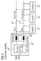
- Fig. 1 shows a typical bus system, as is the prior art. It comprises two bus lines, namely a first bus line 10 * (Abus) and a second bus line 12 * (Bbus). Connected to the bus lines are a plurality of bus devices 14 *. As an example, three bus devices are shown (bus device 1, bus device 2, bus device n), these representing any number n * of bus devices. n * can be very large, eg reach the number 256.
- a power supply 16 * receives via an input a typical mains voltage of 230 V with 50 Hz frequency and converts it in a unit 18 * in a DC voltage of eg between 21 V and 30 V. Decoupling takes place between the unit 18 * and the bus lines 10 * and 12 * (unit 20 *).
- the bus devices 14 * must ensure that the voltage supply and data transmission do not interfere with each other. For example, the data transmission could be damped by the voltage supply in the bus participants and thereby decrease the transmission range.
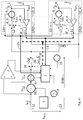
- the ballast off DE-B-10 2008 058 296 is in Fig. 2 shown schematically.
- the reference numbers in this text are identical. However, they are provided with a "*" to distinguish it from the reference numerals of this text.
- Via two input terminals 22 * and 23 * is the bus voltage U bus .
- a current source 40 * Connected in series are a current source 40 *, at which a voltage U DIF drops, and a switch 26 *.
- the current I bus is converted by the current source 40 * to the current I sp .
- the current I SP is measured by a current measuring device 44 ⁇ .
- a node 28 * is provided, which is connected to a further node 29 * via a capacitor C *, which is thus connected in parallel to the inputs 22 * and 23 *.
- Fig. 2 on the right side is at the output 30 * the device voltage U vsp available, namely against ground (ie output 32 *).
- the device according to the technical teaching DE-B-10 2008 058 296 uses the approach that further information is collected via further measuring elements 44 *, 46 *, 34 *, 48 *, which control the current source 40 * via an actuator 42 *. In this case, the temperature of the ballast device and in particular of the current source transistors is detected via a temperature sensor 48 *.
- the output voltage U VSP is detected via a differential amplifier 34 *, which compares the voltage U VSP with an unspecified reference voltage V REF .
- the current measuring device for the load current I VSP is detected by the measuring device 46 * and fed to the adjusting device 42 *.
- the technique disclosed has the disadvantage that, if the load resistance is too low, the current of the current source is limited. As a result, the maximum permitted amount of energy is not taken from the bus, but limits the current. It would be more favorable, however, to make the maximum possible amount of energy available to the consumers until definitely no consumer can be supplied from the bus without violating other higher prioritized conditions, such as operating temperature or maximum energy extraction.
- a bus device with the ballast device according to the invention and a bus system with such bus devices are also provided.
- Individual embodiments of the invention are the subject of the dependent claims.
- the maximum current strength of the bus current is thus limited by the current source to a quasi-static value, for example, programmed by the current of the current supplied by the current source and / or the current flowing through the outputs (load terminals) and / or the voltage applied to the load terminals and / or a temperature measured in or on the bus device is independent and / or independent of at least one time derivative of these quantities (mathematical derivation of the quantity by time).
- the method differs from the one DE-B-10 2008 058 296 , Without further action, however, this would be in exactly the cases where the scheme 38 * DE-B-10 2008 058 296 engages, leading to violation of various conditions.
- the invention is based on the recognition that it makes no sense to specify a maximum current intensity for the bus current I BUS for all situations, but rather to make it dependent on the currently prevailing conditions. These are typically known by the system computers. Therefore, it is also not necessarily useful to perform the default in the ballast itself. In the following it is therefore assumed that the system computers have predetermined a somehow predetermined maximum extraction current I BUSMAX the system according to the invention. In the simplest case, this is a default reset value of this value, which is typically different from zero but may well be zero.
- the basic idea of the method according to the invention is to modify the load instead of the current source by "shedding" loads or parts of loads.
- the load typically consists of several sub-consumers, for which the system according to the invention is a ballast.
- the power source together with its control, ensures that both the slew rate of the bus current I bus and the maximum values of the bus current correspond to the specification of the bus.
- the device according to the invention now has various measuring means which ensure that both the bus specification is not violated and the operating temperature is not exceeded, and that the object according to the invention is also achieved.
- the device according to the invention can have a plurality of loads and thus a plurality of load or output connections 30 *, 32 *. These are designated 9 and 10 for distinction from now on.
- Each load port may be assigned depending on a measurement means for measuring the load current I VSP for the respective load. This is preceded by a switch that can disconnect the load from the intermediate node, without disconnecting the backup capacitor C from the bus.
- a buffer in the control is preferably an energy storage (namely, in particular a capacitor C), which is connected in parallel to the load terminals.
- the invention further includes a bus device with a ballast according to one of the aforementioned embodiments, wherein in the bus device at least one load terminal pair is connected to at least one electrical load, which can be deactivated by the ballast.
- the bus device can be equipped with a ballast according to one of the aforementioned embodiments, wherein in the bus device at least one load terminal pair is connected to at least one electrical load, which can be activated by the ballast.
- At least one electrical load is connected to the bus device, which can be deactivated by the ballast and can simultaneously draw energy from a source of energy other than the bus and its energy intake from this further energy source is at least partially reduced compared to the maximum possible energy consumption from this further energy source when said consumer is deactivated by the ballast with respect to the energy intake from the bus.
- the invention also encompasses a bus system with a bus and a plurality of bus devices connected thereto via terminals, at least one of which has a bus device with one or more of the abovementioned features or a ballast device according to one of the abovementioned embodiments, wherein preferably all bus devices have one Have Vorschalt Surprise.
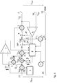
- Vorschalt raised according to the prior art, namely after DE-B-10 2008 058 296 is modified according to the invention as follows (see, for example, the embodiment of Fig. 3 ):
- a current source 16 is used at the location of the previous current source 40 *, which has the property that it can limit the current strength of the bus current I bus to a programmable predetermined value I BUSMAX .
- the previous means 42 * for controlling are replaced by means 1, which have only a pure control function with respect to the power source 16.
- control means 2 are provided for controlling the loads.
- the control means 2 is supplied with a measurement value relating to the current intensity of the current source current I SP transmitted by the current source 16, which is measured by the symbolically represented means 4 for measuring the current intensity.
- means 5 for measuring the current intensity I VSP that is, the output terminal 9 (30 * in FIG Fig. 2 ) and 10 (or GND, 32 * in Fig. 2 ) flowing current.
- the charging current of an energy store can be detected via a further measuring device 15 and made available to the control means 2.
- a measuring instrument 3 may, for example, additionally detect a temperature, for example that of the power transistors of the current source 16, and transmit them to the control means 2. Finally, it makes sense to measure the voltage at the load output U VSP via a voltage measuring device 6, for example an operational amplifier, which is related to a reference voltage V REF , and to make it available to the controller. Finally, it makes sense to detect the power parameters of the current source 16 itself. For this purpose, it makes sense to carry out the measurement of the source current I SP and the power source voltage U DIF . From both the power can be calculated / calculated become. The voltage measurement can be carried out, for example, by an operational amplifier 7 whose output value is made available to the control means 2.
- a separator here exemplified as an additional switch 8, can separate the load from the current source 16 as a function of the parameters thus determined.
- the corresponding control signal 8 'for the separator comes from the controller 2.
- the switch 8 separates the (not shown in the figures) connected to the output terminals 9 and 10 consumers of the energy storage (capacity C).
- the switch 26 into consideration, which is controlled by a control signal 26 'from the control means 2.
- control means 2 can be made dependent on further parameters. For example, it is particularly advantageous if the control means 2 themselves are a finite-state machine or a processor system and can themselves send and receive data and commands via the bus. This is not shown in the figures for clarity.
- a clock in such a control means 2 for example, via the bus at the terminals 22 and 23 for all satellites or bus devices 14 * (see Fig. 1 ) are synchronized.
- the time can now be divided into periods. These can in turn be divided into time slots.
- Each bus device 14 * (see Fig. 1 ), a maximum bus current I BUSMAXk can now be allocated for each time slot k. After the period has expired, the time-first time slot is started again.
- the controller can now switch on and off in dependence on the time slot consumers, namely timeslot controlled, and thus comply with the predetermined I BUS-MAX- run, without the active consumers receive an insufficient supply voltage.
- the I BUSMAX value of the current source does not depend on the measured parameters. Theoretically, the bus to the Input terminals 22,23 of / each bus device thus always the maximum allowable power are removed. However, not all consumers may be operated.
- FIG. 4 a simplified schematic representation of a system with n consumer interfaces.
- the consumer interfaces are numbered 9_1 to 9_n. For simplicity, only the interfaces 1 and n are drawn.
- the other interfaces 2, 3, ... n-1 are indicated by dots.
- the kth interface is considered (k stands for a number between 1 and n).
- the k th interface includes an input 12_k connected to node 28. This can be separated by a separator 8_k from the output 9_k of the k th interface.
- a measuring device 5_k can measure the output current of the interface 9_k.
- the voltage at this point 9_k is detected by a voltage measuring device 6_k.
- this can be an operational amplifier which measures against a reference voltage.
- the other pole 10_k is preferably connected to ground (GND). This is only one possibility. Theoretically, it is of course also conceivable to carry out a separation here, to detect the current and the voltage and to control the configuration thereof by means of the control means 2 and the separating devices 8_1 to 8_n and 26.
- the disconnecting device 8_k of each consumer interface is controlled via a signal 8'_k, which is the k-th signal of the output bus 8 'of the control means 2 for the separation devices 8_1, ..., 8_n provided.
- a deactivation of the load itself can be provided, for example by an "enable” input to the load, which is set to “disabled” by a signal of the control means 2.
- "disabled” means that the load in question preferably consumes or consumes less or less energy from the bus, which is typically reflected in a lower power consumption of the load.
- the control device should also be able to activate the load (the consumer) again when needed.
- the consumer simultaneously receives energy from other sources, it also makes sense to limit this energy intake, so that a reduced energy intake from the bus is usually coupled with a reduced energy intake from other sources.
- the bus 8 'for controlling the load disconnecting devices 8_1 to 8_n is in Fig. 4 dashed lines to be better marked.
- the voltage measuring signal 11_k of the kth consumer interface is connected to the kth line of the voltage measuring bus 11. This voltage measuring bus 11 is guided in the control means 2 and exemplarily serves as one of possibly several input parameter signals.
- the current measurement signal 13_k is supplied to the k-th consumer interface as k-th line of the current measuring bus 13 of the control means 2 and processed similarly.
- FIGS. 3 and 4 are only examples. In the in Fig. 4 shown Vorschalt raiseden are the most important possibilities that provides the present invention, simultaneously and also used in parallel.
- control means 2 for driving a load separation 8 or 8_1 to 8_n receive only the corresponding signals or information from only one of the means 5 or 5_1 to 5_n, 6 or 6_1 to 6_n, 15, 3, 4 for measuring.
- Fig. 5 One last important case is in Fig. 5 shown. It may be useful to omit the switch 26 (this switch is in Fig. 5 however, still drawn) and to use the Strománntransistor the power source 16 as a switch for dropping the downstream loads. This can for example be done by the control means 2 fixed by an additional switch 17, the control line of the power source 16 to such a potential that the power source 16 is high impedance and thus turns off. In this case, it is also useful to supply the parts 18 of the ballast, which must be absolutely ready to communicate, by switching with a second additional switch 19 no longer from the now off power source 16, but directly from the bus. Optionally, then an optional resistor 20 a short circuit in this part 18 of the ballast comply with buss specification.
- these parts 18 continue with the central bus power supply 16 * (see Fig. 1 ) or a bus master, even if the current source current I SP is set to zero.
- the bus master can cause other bus subscribers to draw less power and thus provide more power to the bus device with a fault condition.
- the affected bus device prior to the dropping of loads warn the bus master and, for example, only after a predetermined time or the presence of other conditions, the loads if necessary immediately or even gradually thrown off.
- the loads if necessary immediately or even gradually thrown off.
- more bus devices can be operated on the bus than specified, since they do not require the same amount of power continuously.
- the means 1 for controlling the current source 16 may be expedient for the means 1 for controlling the current source 16 to receive a signal from a device 24 for measuring the current I bus and thus to control the current source 16 in such a way that the current I bus corresponds to the current of the current source 16, regardless of which power other network elements, such as voltage sources, resistors or the resistor 25, measuring amplifier, in addition to the power source 16 feed (see Fig. 6 ).
- the advantage of this approach is, for example, that parasitic currents of the network of, for example, the means 4 for measuring the current I SP , the potential measuring device 7 for measuring U DIF , the means 5 for measuring the current I VSP , the potential measuring device 6 for measuring U VSP and / or the device 15 for measuring the charging current I C of the capacitor C, in compliance with the exact current I bus to be considered, which increases the precision of the maximum current compliance, as for example from the bus standard or from the bus Protocol may be required.
Landscapes
- Engineering & Computer Science (AREA)
- Computer Networks & Wireless Communication (AREA)
- Signal Processing (AREA)
- Power Engineering (AREA)
- Direct Current Feeding And Distribution (AREA)
- Remote Monitoring And Control Of Power-Distribution Networks (AREA)
Claims (18)
- Procédé de mise à disposition de courant pour au moins un consommateur connecté à un dispositif de bus, le dispositif de bus étant connecté au bus via deux bornes d'entrée (22, 23) et au moins une source de courant (4) à commande étant montée en aval de l'une des bornes d'entrée (22), laquelle met à disposition, sur un côté orienté vers au moins un consommateur, un courant de source de courant (ISP) et reçoit à cet effet du côté de la borne d'entrée (22) un courant de bus (IBUS) et une tension (UBUS), un courant de charge (IVSP) fonction du courant de source de courant (ISP) passant par l'ensemble des consommateurs et un courant de charge (IVSP) respectivement correspondant passant par un consommateur individuel, une tension de charge (UVSP) étant présente à des bornes de sortie (9, 10) pour au moins un consommateur et un dispositif de coupure de charge (8, 8_1 à 8_n, 16, 26) étant prévu pour couper et/ou désactiver au moins une partie du consommateur,
caractérisé en ce que
la coupure et/ou la désactivation d'au moins une partie du consommateur est effectuéei. en fonction de l'intensité de courant (ISP) d'au moins un courant de source de courant ou en fonction d'au moins une dérivée par rapport au temps de ces grandeurs ouii. en fonction d'au moins une intensité de courant de charge (IVSP) ou en fonction d'au moins une dérivée par rapport au temps de ces grandeurs ouiii. en fonction d'une température (T) mesurée dans ou sur le dispositif de bus ou en fonction d'au moins une dérivée par rapport au temps de ces grandeurs. - Procédé selon la revendication 1, caractérisé en ce qu'au moins une source de courant (16) et/ou au moins un commutateur (8, 8_1, à 8_n, 26) sont utilisés comme dispositif de coupure de charge.
- Procédé selon la revendication 2, caractérisé en ce que, pendant au moins une partie du temps de coupure d'une partie du consommateur, des parties (18) du dispositif de bus sont alimentées directement à partir du bus en contournant la (ou les) source(s) de courant.
- Procédé selon la revendication 3, caractérisé en ce que des parties du dispositif de bus qui sont aptes à être alimentées directement à partir du bus, sont conçues pour neutraliser une coupure de la source de courant.
- Procédé selon l'une des revendications 1 à 4, caractérisé en ce que le courant (IBUS) pris du bus après coupure des sources de courant (16) n'est pas limité par un dispositif technique.
- Procédé selon l'une des revendications 1 à 5, caractérisé en ce que des parties qui, en cas de coupure de la source de courant (16), sont alimentées directement à partir du bus, le sont dans d'autres cas où au moins une source de courant (16) n'est pas coupée, via au moins une de ces sources de courant non coupées (16) qui reçoit son énergie à partir du bus.
- Procédé selon l'une des revendications 1 à 6, caractérisé en ce que, en cas de présence un accumulateur d'énergie, notamment sous la forme d'un condensateur (C), le dispositif de coupure de courant (8, 8_1 à 8_n, 16, 26) est disposé entre l'accumulateur d'énergie et les bornes de sortie (9, 10) du dispositif de bus.
- Dispositif d'entrée pour un consommateur conçu pour être connecté à un dispositif de bus, le dispositif de bus étant pourvu de deux bornes d'entrée (22, 23) pour la connexion du dispositif de bus à un bus et d'au moins une paire de bornes de charge (9, 9_1 à 9_n, 10, 10_1 à 10_n) pour la connexion d'au moins un consommateur électrique, chaque paire de bornes de charge (9, 9_1 à 9_n, 10, 10_1 à 10_n) étant couplée à au moins une borne d'entrée (22, 23), et dans la connexion d'une première borne d'entrée (22) à une première borne de charge (9, 9_1 à 9_n) d'au moins une paire de bornes de charge (9, 9_1 à 9_n, 10, 10_1 à 10_n) étant disposés une source de courant (16) et au moins un dispositif de coupure de charge (8, 8_1 à 8_n, 16, 26) apte à être commandé par des moyens de commande (2) pour la coupure et/ou la désactivation d'au moins une partie du consommateur, qui est conçu pour couper et/ou désactiver électriquement un consommateur connecté à ladite paire de bornes de charge (9, 9_1 à 9_n, 10, 10_1 à 10_n), et les moyens de commande (2) étant conçus pour obtenir que les dispositifs de coupure de charge (8, 8_1 à 8_n, 16, 26) changent le débit d'énergie du dispositif d'entrée vers ledit au moins un consommateur monté en aval et/ou la réception d'énergie provenant du bus par le dispositif d'entrée et ledit au moins un consommateur monté en aval, respectivement par coupure de charge et/ou désactivation,
caractérisé en ce que
l'envergure et la nature de la coupure de charge et/ou de la désactivation sont fonction d'une grandeur prédéterminée qui est comprise dans le groupe comprenantA) l'intensité de courant (ISPMAX) prédéterminée du courant (ISP) débité par la source de courant (16) ou une dérivée par rapport au temps de cette grandeur ouB) au moins une intensité de courant de charge (IVSP1 à IVSPn) ou une dérivée par rapport au temps de cette grandeur ouC) la température (T) de parties du dispositif d'entrée ou aux alentours du dispositif d'entrée, notamment des transistors de puissance de la source de courant ou une dérivée par rapport au temps de la température. - Dispositif d'entrée selon la revendication 8, caractérisé en ce qu'au moins une source de courant (16) remplit, en plus de la fonction de source de courant, la fonction d'un dispositif de coupure de charge et/ou au moins un commutateur remplit la fonction de dispositif de coupure de charge.
- Dispositif d'entrée selon la revendication 8 ou 9, comprenant en outre des moyens (5, 5_1 à 5_n, 6, 6_1 à 6_n, 15, 3, 4) pour mesurer la grandeur prédéterminée selon la caractéristique il, qui sont couplés avec les moyens de commande (2).
- Dispositif d'entrée selon l'une des revendications 8 à 10, comprenant en outre au moins un accumulateur d'énergie (C) pour une alimentation au moins temporairement possible d'au moins une paire de bornes de charge (10_i et 9_i avec 0<i<n+1), notamment sous la forme d'un condensateur (C) monté parallèlement à ladite au moins une paire de bornes de charge (10_i et 9_i avec 0<i<n+1).
- Dispositif d'entrée selon la revendication 11, caractérisé en ce que le dispositif de coupure de charge (8, 8_1 à 8_n, 16, 26) comprend un premier et un deuxième commutateurs qui sont montés en série et entre lesquels est disposé un noeud auquel le condensateur (C) est couplé.
- Dispositif d'entrée selon l'une des revendications 8 à 12, caractérisé en ce que, au cas où le courant (ISP) d'au moins une source de courant (16) est mis à zéro, des parties (18) du dispositif d'entrée continuent à être alimentés en énergie à partir du bus, notamment via une résistance (20) qui peut aussi être zéro.
- Dispositif d'entrée selon l'une des revendications 8 à 13, caractérisé en ce que le moyen (1) pour commander la source de courant (16) reçoit un signal d'un dispositif (24) pour mesurer le courant (IBUS) et commande la source de courant (16) avec celui-ci d'une manière telle que le courant (IBUS) corresponde au courant fourni par la source de courant (16) et soit sensiblement égal à ce courant, et cela indépendamment de la question de savoir quelle quantité de courant d'autres élément du réseau (22, 25) tels que, par exemple, des sources de tension, des résistances, des amplificateurs de mesure, contribuent en plus de la source de courant (16).
- Dispositif d'entrée selon l'une des revendications 8 à 14, caractérisé en ce qu'au moins une des parties (18) du dispositif d'entrée qui continuent, après coupure d'au moins une source de courant (16) et/ou de toutes les sources de courant (16, 22), à être alimentées en énergie à partir du bus, est conçue pour arrêter cet état de coupure.
- Dispositif de bus avec un dispositif d'entrée selon l'une des revendications 8 à 15, au moins un consommateur électrique étant connecté dans le dispositif de bus à au moins une paire de bornes de charge (9, 9_1 à 9_n, 10, 10_1 à 10_n).
- Dispositif de bus avec un dispositif d'entrée selon l'une des revendications 8 à 15, dans le dispositif de bus, à au moins une paire de bornes de charge (9, 9_1 à 9_n, 10, 10_1 à 10_n), étant connecté au moins un consommateur électrique qui est conçu pour pouvoir être désactivé et/ou activé par le dispositif d'entrée et/ou qui, en même temps, peut recevoir de l'énergie à partir d'une autre source d'énergie que le bus et dont la consommation de l'énergie provenant de cette source d'énergie est au moins temporairement réduite par rapport à la consommation maximalement possible d'énergie provenant de cette source d'énergie lorsque ledit consommateur est désactivé par le dispositif d'entrée en ce qui concerne la consommation d'énergie.
- Système de bus avec un bus ou une pluralité de dispositifs de bus y connectés via des bornes (22, 23) dont au moins un dispositif de bus est conforme à une des revendications 16 ou 17 ou qui comprend un dispositif d'entrée selon une des revendications 8 à 15.
Priority Applications (1)
| Application Number | Priority Date | Filing Date | Title |
|---|---|---|---|
| EP14154301.7A EP2765713B1 (fr) | 2013-02-08 | 2014-02-07 | Procédé de mise à disposition de courant pour au moins un consommateur raccordé à un bus et dispositif d'entrée pour un consommateur |
Applications Claiming Priority (2)
| Application Number | Priority Date | Filing Date | Title |
|---|---|---|---|
| EP13154618 | 2013-02-08 | ||
| EP14154301.7A EP2765713B1 (fr) | 2013-02-08 | 2014-02-07 | Procédé de mise à disposition de courant pour au moins un consommateur raccordé à un bus et dispositif d'entrée pour un consommateur |
Publications (2)
| Publication Number | Publication Date |
|---|---|
| EP2765713A1 EP2765713A1 (fr) | 2014-08-13 |
| EP2765713B1 true EP2765713B1 (fr) | 2016-11-30 |
Family
ID=47739079
Family Applications (1)
| Application Number | Title | Priority Date | Filing Date |
|---|---|---|---|
| EP14154301.7A Active EP2765713B1 (fr) | 2013-02-08 | 2014-02-07 | Procédé de mise à disposition de courant pour au moins un consommateur raccordé à un bus et dispositif d'entrée pour un consommateur |
Country Status (1)
| Country | Link |
|---|---|
| EP (1) | EP2765713B1 (fr) |
Families Citing this family (4)
| Publication number | Priority date | Publication date | Assignee | Title |
|---|---|---|---|---|
| DE102015208495A1 (de) * | 2015-05-07 | 2016-11-10 | Continental Automotive Gmbh | Steuerelektronik für ein land- oder forstwirtschaftliches Fahrzeug |
| DE102018010305C5 (de) * | 2018-09-10 | 2026-02-19 | Inova Semiconductors Gmbh | Segmentierte Steuerungsanordnung |
| DE102018007141C5 (de) * | 2018-09-10 | 2025-05-15 | Inova Semiconductors Gmbh | Segmentierte Steuerungsanordnung |
| DE102018132024A1 (de) | 2018-12-13 | 2020-06-18 | Valeo Schalter Und Sensoren Gmbh | Netzwerkkommunikationssystem mit bidirektionaler Strommodulation zur Datenübertragung |
Family Cites Families (4)
| Publication number | Priority date | Publication date | Assignee | Title |
|---|---|---|---|---|
| DE10147924B4 (de) * | 2001-09-28 | 2006-03-09 | Siemens Ag | Verfahren und Einrichtung zur übertragerlosen Spannungsversorgung |
| DE102005002753B4 (de) | 2005-01-20 | 2006-12-07 | Siemens Ag | Spannungsversorgungsvorrichtung für ein Busgerät und entsprechendes Betriebsverfahren |
| DE102006032797B4 (de) * | 2006-07-14 | 2012-10-11 | Siemens Ag | Verfahren zum Regeln einer Busgerätespannung und Vorschalteinrichtung |
| DE102008058296B4 (de) | 2008-11-20 | 2011-03-10 | Siemens Aktiengesellschaft | Verfahren zum Bereitstellen von Strom für Verbraucher in einem Busgerät sowie Vorschalteinrichtung |
-
2014
- 2014-02-07 EP EP14154301.7A patent/EP2765713B1/fr active Active
Non-Patent Citations (1)
| Title |
|---|
| None * |
Also Published As
| Publication number | Publication date |
|---|---|
| EP2765713A1 (fr) | 2014-08-13 |
Similar Documents
| Publication | Publication Date | Title |
|---|---|---|
| EP3461069B1 (fr) | Procédé d'attribution d'adresses dans un système de bus de données série et noeuds de bus pour un tel système de bus de données série | |
| EP3493481B1 (fr) | Procédé d'alimentation de flux d'adressage au moyen des n uds de bus d'un système de bus de données série et n uds de bus pour un tel système de bus de données | |
| EP3496341B1 (fr) | Procédé de commande d'un système de base de données série et noeuds de bus pour un tel système de base de données | |
| EP2007077A1 (fr) | Procédé de détermination de la position d'appareils esclaves dans une commutation en série et appareil esclave pour des commutations en série | |
| EP3146605A1 (fr) | Procédé permettant de faire fonctionner un réseau de bord d'un véhicule automobile et véhicule automobile | |
| DE102006001984A1 (de) | Verfahren und Vorrichtung zur Bereitstellung einer Versorgungsspannung mittels parallel geschalteter Generatoreinheiten | |
| EP3351056B1 (fr) | Unité d'alimentation d'un bus | |
| EP2765713A1 (fr) | Procédé de mise à disposition de courant pour au moins un consommateur raccordé à un bus et dispositif d'entrée pour un consommateur | |
| EP3224894A1 (fr) | Procédé d'équilibrage d'un système de stockage d'énergie | |
| DE102016201390A1 (de) | Versorgungseinheit für einen Bus | |
| DE102012100673A1 (de) | Vorrichtung zur elektrischen Energieeinspeisung aus einer dezentralen Eigenerzeugeranlage in ein Stromnetz | |
| EP2190094B1 (fr) | Procédé de préparation de courant pour consommateurs dans un appareil de bus et dispositif d'entrée | |
| EP2093848A2 (fr) | Prise pour la connexion électrique d'une remorque sur un véhicule de traction | |
| EP2437228B1 (fr) | Alarme, installation d'alarme et procédé de reconnaissance d'erreurs de lignes de transmission | |
| EP1702808A2 (fr) | Dispositif d'alimentation de tension pour des consommateurs dans une réseau de bord d' un véhicule utilisant plusieurs générateurs | |
| DE102021119956A1 (de) | Testen von Stromversorgungspfaden und Verbrauchern eines Fahrzeugs | |
| WO2025104142A1 (fr) | Dispositif de sécurité électrique et procédé pour faire fonctionner un dispositif de sécurité électrique | |
| DE102013109544A1 (de) | Aufwachschaltung für elektronische Geräte | |
| DE102014116920A1 (de) | Interrupt-Schutz-Schaltungen, Systeme und Verfahren für Sensoren und andere Bauelemente | |
| AT17944U1 (de) | Bus-Zentraleinheit mit Power Monitoring | |
| DE102012217447B4 (de) | Verfahren zum Steuern einer Ladevorrichtung und dafür angepasste Ladevorrichtung | |
| DE19910015B4 (de) | Verfahren und Vorrichtung zur Verlängerung der Pufferzeit eines Uhrenschaltkreises | |
| DE102009058316A1 (de) | Vorrichtung zum Erzeugen einer gestützten Gleichspannung | |
| EP3582340A1 (fr) | Raccord d'appareil d'adapté | |
| DE102023116304A1 (de) | Lichtbogenvermeidung an einem usb-anschluss |
Legal Events
| Date | Code | Title | Description |
|---|---|---|---|
| PUAI | Public reference made under article 153(3) epc to a published international application that has entered the european phase |
Free format text: ORIGINAL CODE: 0009012 |
|
| 17P | Request for examination filed |
Effective date: 20140207 |
|
| AK | Designated contracting states |
Kind code of ref document: A1 Designated state(s): AL AT BE BG CH CY CZ DE DK EE ES FI FR GB GR HR HU IE IS IT LI LT LU LV MC MK MT NL NO PL PT RO RS SE SI SK SM TR |
|
| AX | Request for extension of the european patent |
Extension state: BA ME |
|
| R17P | Request for examination filed (corrected) |
Effective date: 20150130 |
|
| RBV | Designated contracting states (corrected) |
Designated state(s): AL AT BE BG CH CY CZ DE DK EE ES FI FR GB GR HR HU IE IS IT LI LT LU LV MC MK MT NL NO PL PT RO RS SE SI SK SM TR |
|
| RAP1 | Party data changed (applicant data changed or rights of an application transferred) |
Owner name: ELMOS SEMICONDUCTOR AKTIENGESELLSCHAFT |
|
| RAP1 | Party data changed (applicant data changed or rights of an application transferred) |
Owner name: ELMOS SEMICONDUCTOR AKTIENGESELLSCHAFT |
|
| GRAP | Despatch of communication of intention to grant a patent |
Free format text: ORIGINAL CODE: EPIDOSNIGR1 |
|
| INTG | Intention to grant announced |
Effective date: 20160621 |
|
| GRAS | Grant fee paid |
Free format text: ORIGINAL CODE: EPIDOSNIGR3 |
|
| GRAA | (expected) grant |
Free format text: ORIGINAL CODE: 0009210 |
|
| AK | Designated contracting states |
Kind code of ref document: B1 Designated state(s): AL AT BE BG CH CY CZ DE DK EE ES FI FR GB GR HR HU IE IS IT LI LT LU LV MC MK MT NL NO PL PT RO RS SE SI SK SM TR |
|
| REG | Reference to a national code |
Ref country code: CH Ref legal event code: EP Ref country code: GB Ref legal event code: FG4D Free format text: NOT ENGLISH |
|
| REG | Reference to a national code |
Ref country code: AT Ref legal event code: REF Ref document number: 850683 Country of ref document: AT Kind code of ref document: T Effective date: 20161215 |
|
| REG | Reference to a national code |
Ref country code: IE Ref legal event code: FG4D Free format text: LANGUAGE OF EP DOCUMENT: GERMAN |
|
| REG | Reference to a national code |
Ref country code: DE Ref legal event code: R096 Ref document number: 502014002060 Country of ref document: DE |
|
| REG | Reference to a national code |
Ref country code: FR Ref legal event code: PLFP Year of fee payment: 4 |
|
| PG25 | Lapsed in a contracting state [announced via postgrant information from national office to epo] |
Ref country code: LV Free format text: LAPSE BECAUSE OF FAILURE TO SUBMIT A TRANSLATION OF THE DESCRIPTION OR TO PAY THE FEE WITHIN THE PRESCRIBED TIME-LIMIT Effective date: 20161130 |
|
| REG | Reference to a national code |
Ref country code: LT Ref legal event code: MG4D |
|
| REG | Reference to a national code |
Ref country code: NL Ref legal event code: MP Effective date: 20161130 |
|
| PG25 | Lapsed in a contracting state [announced via postgrant information from national office to epo] |
Ref country code: SE Free format text: LAPSE BECAUSE OF FAILURE TO SUBMIT A TRANSLATION OF THE DESCRIPTION OR TO PAY THE FEE WITHIN THE PRESCRIBED TIME-LIMIT Effective date: 20161130 Ref country code: NO Free format text: LAPSE BECAUSE OF FAILURE TO SUBMIT A TRANSLATION OF THE DESCRIPTION OR TO PAY THE FEE WITHIN THE PRESCRIBED TIME-LIMIT Effective date: 20170228 Ref country code: LT Free format text: LAPSE BECAUSE OF FAILURE TO SUBMIT A TRANSLATION OF THE DESCRIPTION OR TO PAY THE FEE WITHIN THE PRESCRIBED TIME-LIMIT Effective date: 20161130 Ref country code: GR Free format text: LAPSE BECAUSE OF FAILURE TO SUBMIT A TRANSLATION OF THE DESCRIPTION OR TO PAY THE FEE WITHIN THE PRESCRIBED TIME-LIMIT Effective date: 20170301 |
|
| PG25 | Lapsed in a contracting state [announced via postgrant information from national office to epo] |
Ref country code: ES Free format text: LAPSE BECAUSE OF FAILURE TO SUBMIT A TRANSLATION OF THE DESCRIPTION OR TO PAY THE FEE WITHIN THE PRESCRIBED TIME-LIMIT Effective date: 20161130 Ref country code: FI Free format text: LAPSE BECAUSE OF FAILURE TO SUBMIT A TRANSLATION OF THE DESCRIPTION OR TO PAY THE FEE WITHIN THE PRESCRIBED TIME-LIMIT Effective date: 20161130 Ref country code: PT Free format text: LAPSE BECAUSE OF FAILURE TO SUBMIT A TRANSLATION OF THE DESCRIPTION OR TO PAY THE FEE WITHIN THE PRESCRIBED TIME-LIMIT Effective date: 20170330 Ref country code: BE Free format text: LAPSE BECAUSE OF NON-PAYMENT OF DUE FEES Effective date: 20170228 Ref country code: PL Free format text: LAPSE BECAUSE OF FAILURE TO SUBMIT A TRANSLATION OF THE DESCRIPTION OR TO PAY THE FEE WITHIN THE PRESCRIBED TIME-LIMIT Effective date: 20161130 Ref country code: RS Free format text: LAPSE BECAUSE OF FAILURE TO SUBMIT A TRANSLATION OF THE DESCRIPTION OR TO PAY THE FEE WITHIN THE PRESCRIBED TIME-LIMIT Effective date: 20161130 Ref country code: HR Free format text: LAPSE BECAUSE OF FAILURE TO SUBMIT A TRANSLATION OF THE DESCRIPTION OR TO PAY THE FEE WITHIN THE PRESCRIBED TIME-LIMIT Effective date: 20161130 |
|
| PG25 | Lapsed in a contracting state [announced via postgrant information from national office to epo] |
Ref country code: NL Free format text: LAPSE BECAUSE OF FAILURE TO SUBMIT A TRANSLATION OF THE DESCRIPTION OR TO PAY THE FEE WITHIN THE PRESCRIBED TIME-LIMIT Effective date: 20161130 |
|
| PG25 | Lapsed in a contracting state [announced via postgrant information from national office to epo] |
Ref country code: RO Free format text: LAPSE BECAUSE OF FAILURE TO SUBMIT A TRANSLATION OF THE DESCRIPTION OR TO PAY THE FEE WITHIN THE PRESCRIBED TIME-LIMIT Effective date: 20161130 Ref country code: SK Free format text: LAPSE BECAUSE OF FAILURE TO SUBMIT A TRANSLATION OF THE DESCRIPTION OR TO PAY THE FEE WITHIN THE PRESCRIBED TIME-LIMIT Effective date: 20161130 Ref country code: CZ Free format text: LAPSE BECAUSE OF FAILURE TO SUBMIT A TRANSLATION OF THE DESCRIPTION OR TO PAY THE FEE WITHIN THE PRESCRIBED TIME-LIMIT Effective date: 20161130 Ref country code: DK Free format text: LAPSE BECAUSE OF FAILURE TO SUBMIT A TRANSLATION OF THE DESCRIPTION OR TO PAY THE FEE WITHIN THE PRESCRIBED TIME-LIMIT Effective date: 20161130 Ref country code: EE Free format text: LAPSE BECAUSE OF FAILURE TO SUBMIT A TRANSLATION OF THE DESCRIPTION OR TO PAY THE FEE WITHIN THE PRESCRIBED TIME-LIMIT Effective date: 20161130 |
|
| PG25 | Lapsed in a contracting state [announced via postgrant information from national office to epo] |
Ref country code: SM Free format text: LAPSE BECAUSE OF FAILURE TO SUBMIT A TRANSLATION OF THE DESCRIPTION OR TO PAY THE FEE WITHIN THE PRESCRIBED TIME-LIMIT Effective date: 20161130 Ref country code: IT Free format text: LAPSE BECAUSE OF FAILURE TO SUBMIT A TRANSLATION OF THE DESCRIPTION OR TO PAY THE FEE WITHIN THE PRESCRIBED TIME-LIMIT Effective date: 20161130 Ref country code: BG Free format text: LAPSE BECAUSE OF FAILURE TO SUBMIT A TRANSLATION OF THE DESCRIPTION OR TO PAY THE FEE WITHIN THE PRESCRIBED TIME-LIMIT Effective date: 20170228 |
|
| REG | Reference to a national code |
Ref country code: DE Ref legal event code: R097 Ref document number: 502014002060 Country of ref document: DE |
|
| PG25 | Lapsed in a contracting state [announced via postgrant information from national office to epo] |
Ref country code: MC Free format text: LAPSE BECAUSE OF FAILURE TO SUBMIT A TRANSLATION OF THE DESCRIPTION OR TO PAY THE FEE WITHIN THE PRESCRIBED TIME-LIMIT Effective date: 20161130 |
|
| REG | Reference to a national code |
Ref country code: CH Ref legal event code: PL |
|
| PLBE | No opposition filed within time limit |
Free format text: ORIGINAL CODE: 0009261 |
|
| STAA | Information on the status of an ep patent application or granted ep patent |
Free format text: STATUS: NO OPPOSITION FILED WITHIN TIME LIMIT |
|
| PG25 | Lapsed in a contracting state [announced via postgrant information from national office to epo] |
Ref country code: LI Free format text: LAPSE BECAUSE OF NON-PAYMENT OF DUE FEES Effective date: 20170228 Ref country code: CH Free format text: LAPSE BECAUSE OF NON-PAYMENT OF DUE FEES Effective date: 20170228 |
|
| 26N | No opposition filed |
Effective date: 20170831 |
|
| REG | Reference to a national code |
Ref country code: IE Ref legal event code: MM4A |
|
| PG25 | Lapsed in a contracting state [announced via postgrant information from national office to epo] |
Ref country code: SI Free format text: LAPSE BECAUSE OF FAILURE TO SUBMIT A TRANSLATION OF THE DESCRIPTION OR TO PAY THE FEE WITHIN THE PRESCRIBED TIME-LIMIT Effective date: 20161130 |
|
| PG25 | Lapsed in a contracting state [announced via postgrant information from national office to epo] |
Ref country code: LU Free format text: LAPSE BECAUSE OF NON-PAYMENT OF DUE FEES Effective date: 20170207 |
|
| REG | Reference to a national code |
Ref country code: BE Ref legal event code: MM Effective date: 20170228 |
|
| REG | Reference to a national code |
Ref country code: FR Ref legal event code: PLFP Year of fee payment: 5 |
|
| PG25 | Lapsed in a contracting state [announced via postgrant information from national office to epo] |
Ref country code: IE Free format text: LAPSE BECAUSE OF NON-PAYMENT OF DUE FEES Effective date: 20170207 |
|
| PG25 | Lapsed in a contracting state [announced via postgrant information from national office to epo] |
Ref country code: MT Free format text: LAPSE BECAUSE OF FAILURE TO SUBMIT A TRANSLATION OF THE DESCRIPTION OR TO PAY THE FEE WITHIN THE PRESCRIBED TIME-LIMIT Effective date: 20161130 |
|
| GBPC | Gb: european patent ceased through non-payment of renewal fee |
Effective date: 20180207 |
|
| PG25 | Lapsed in a contracting state [announced via postgrant information from national office to epo] |
Ref country code: GB Free format text: LAPSE BECAUSE OF NON-PAYMENT OF DUE FEES Effective date: 20180207 |
|
| PG25 | Lapsed in a contracting state [announced via postgrant information from national office to epo] |
Ref country code: HU Free format text: LAPSE BECAUSE OF FAILURE TO SUBMIT A TRANSLATION OF THE DESCRIPTION OR TO PAY THE FEE WITHIN THE PRESCRIBED TIME-LIMIT; INVALID AB INITIO Effective date: 20140207 |
|
| PG25 | Lapsed in a contracting state [announced via postgrant information from national office to epo] |
Ref country code: CY Free format text: LAPSE BECAUSE OF NON-PAYMENT OF DUE FEES Effective date: 20161130 |
|
| PG25 | Lapsed in a contracting state [announced via postgrant information from national office to epo] |
Ref country code: MK Free format text: LAPSE BECAUSE OF FAILURE TO SUBMIT A TRANSLATION OF THE DESCRIPTION OR TO PAY THE FEE WITHIN THE PRESCRIBED TIME-LIMIT Effective date: 20161130 |
|
| PG25 | Lapsed in a contracting state [announced via postgrant information from national office to epo] |
Ref country code: TR Free format text: LAPSE BECAUSE OF FAILURE TO SUBMIT A TRANSLATION OF THE DESCRIPTION OR TO PAY THE FEE WITHIN THE PRESCRIBED TIME-LIMIT Effective date: 20161130 |
|
| REG | Reference to a national code |
Ref country code: AT Ref legal event code: MM01 Ref document number: 850683 Country of ref document: AT Kind code of ref document: T Effective date: 20190207 |
|
| PG25 | Lapsed in a contracting state [announced via postgrant information from national office to epo] |
Ref country code: AT Free format text: LAPSE BECAUSE OF NON-PAYMENT OF DUE FEES Effective date: 20190207 |
|
| PG25 | Lapsed in a contracting state [announced via postgrant information from national office to epo] |
Ref country code: AL Free format text: LAPSE BECAUSE OF FAILURE TO SUBMIT A TRANSLATION OF THE DESCRIPTION OR TO PAY THE FEE WITHIN THE PRESCRIBED TIME-LIMIT Effective date: 20161130 Ref country code: IS Free format text: LAPSE BECAUSE OF FAILURE TO SUBMIT A TRANSLATION OF THE DESCRIPTION OR TO PAY THE FEE WITHIN THE PRESCRIBED TIME-LIMIT Effective date: 20170330 |
|
| REG | Reference to a national code |
Ref country code: DE Ref legal event code: R082 Ref document number: 502014002060 Country of ref document: DE Representative=s name: DOMPATENT VON KREISLER SELTING WERNER - PARTNE, DE Ref country code: DE Ref legal event code: R081 Ref document number: 502014002060 Country of ref document: DE Owner name: ELMOS SEMICONDUCTOR SE, DE Free format text: FORMER OWNER: ELMOS SEMICONDUCTOR AKTIENGESELLSCHAFT, 44227 DORTMUND, DE |
|
| P01 | Opt-out of the competence of the unified patent court (upc) registered |
Effective date: 20230525 |
|
| REG | Reference to a national code |
Ref country code: DE Ref legal event code: R081 Ref document number: 502014002060 Country of ref document: DE Owner name: ELMOS SEMICONDUCTOR SE, DE Free format text: FORMER OWNER: ELMOS SEMICONDUCTOR SE, 44227 DORTMUND, DE |
|
| PGFP | Annual fee paid to national office [announced via postgrant information from national office to epo] |
Ref country code: DE Payment date: 20260217 Year of fee payment: 13 |
|
| PGFP | Annual fee paid to national office [announced via postgrant information from national office to epo] |
Ref country code: FR Payment date: 20260223 Year of fee payment: 13 |