EP2765745B1 - Bus-Kommunikationssendeempfänger - Google Patents
Bus-Kommunikationssendeempfänger Download PDFInfo
- Publication number
- EP2765745B1 EP2765745B1 EP14153770.4A EP14153770A EP2765745B1 EP 2765745 B1 EP2765745 B1 EP 2765745B1 EP 14153770 A EP14153770 A EP 14153770A EP 2765745 B1 EP2765745 B1 EP 2765745B1
- Authority
- EP
- European Patent Office
- Prior art keywords
- signal
- output
- bus
- voltage
- delay time
- Prior art date
- Legal status (The legal status is an assumption and is not a legal conclusion. Google has not performed a legal analysis and makes no representation as to the accuracy of the status listed.)
- Active
Links
Images



Classifications
-
- H—ELECTRICITY
- H04—ELECTRIC COMMUNICATION TECHNIQUE
- H04L—TRANSMISSION OF DIGITAL INFORMATION, e.g. TELEGRAPHIC COMMUNICATION
- H04L25/00—Baseband systems
- H04L25/02—Details ; arrangements for supplying electrical power along data transmission lines
- H04L25/026—Arrangements for coupling transmitters, receivers or transceivers to transmission lines; Line drivers
-
- H—ELECTRICITY
- H03—ELECTRONIC CIRCUITRY
- H03K—PULSE TECHNIQUE
- H03K6/00—Manipulating pulses having a finite slope and not covered by one of the other main groups of this subclass
- H03K6/04—Modifying slopes of pulses, e.g. S-correction
-
- H—ELECTRICITY
- H04—ELECTRIC COMMUNICATION TECHNIQUE
- H04L—TRANSMISSION OF DIGITAL INFORMATION, e.g. TELEGRAPHIC COMMUNICATION
- H04L25/00—Baseband systems
- H04L25/02—Details ; arrangements for supplying electrical power along data transmission lines
- H04L25/06—DC level restoring means; Bias distortion correction ; Decision circuits providing symbol by symbol detection
-
- H—ELECTRICITY
- H04—ELECTRIC COMMUNICATION TECHNIQUE
- H04L—TRANSMISSION OF DIGITAL INFORMATION, e.g. TELEGRAPHIC COMMUNICATION
- H04L7/00—Arrangements for synchronising receiver with transmitter
-
- H—ELECTRICITY
- H04—ELECTRIC COMMUNICATION TECHNIQUE
- H04L—TRANSMISSION OF DIGITAL INFORMATION, e.g. TELEGRAPHIC COMMUNICATION
- H04L7/00—Arrangements for synchronising receiver with transmitter
- H04L7/0016—Arrangements for synchronising receiver with transmitter correction of synchronization errors
- H04L7/0045—Correction by a latch cascade
Definitions
- the present invention is related to a bus communication transceiver, and more particularly, a bus communication transceiver which can be connected with a single wire bus.
- a network protocol used when communication is carried out through a single wire bus such as LIN (Local Interconnect Network) is known.
- LIN Local Interconnect Network
- the network is mainly installed on a car and is used to control various devices such as a door mirror and a door lock.
- the waveform of a signal to be inputted and outputted to or from the bus is standardized to meet various conditions.
- a duty ratio is contained in these conditions and the duty ratio is a ratio of a time for the signal to be higher than a predetermined voltage and a time for the signal to be lower than the predetermined voltage.
- the duty ratio varies according to a change of the environment of the LIN, and there is a case that the signal waveform comes off a range of the standard.
- a car-mounted battery is used as a power supply to supply a bus with a voltage. It is known that the power supply voltage of the car-mounted battery varies largely between 7 V and 18 V while a charging operation or a discharging operation is carried out, even when a ruled voltage is 12 V. Also, a variation of the duty ratio is sometimes caused through a variation of the total load connected with the bus.
- Patent Literature 1 discloses an output circuit of an LSI.
- the output circuit of the LSI detects a dull waveform at the time of rising of a signal and the time of falling thereof and adjusts the waveform of the next signal based on the detection result.
- US 2002/017930 A1 relates to a signal transmission device having, compared with a conventional signal transmission device, additionally a waveform adjustment circuit that controls the delay time produced by a timing adjustment circuit according to changes in the states of control signals.
- the conventional signal transmission device that transmits signals fed thereto to another device through a transformer
- the timing with which the switching device that has been receiving current up to the moment is turned off is delayed from the timing with which the other switching devices are turned on or off to reduce overshoots and undershoots.
- US 6 366 115 B1 relates to a buffer circuit including a delay circuit which is interposed between a signal source and a following circuit.
- the delay circuit propagates a signal from an input to an output; the signal has associated desired timing relationships between its rising and falling edges.
- the delay circuit controls the propagation delays of the signal's rising and falling edges such that when the signal arrives at a selected downstream node, it has the desired timing relationships.
- the delay circuit adjusts the propagation delays in accordance with two correction signals: one which reduces errors induced by imperfections in the signal path through which the test signal propagates, and one to reduce errors due to thermal effects that arise when propagating a periodic test signal having a duty cycle other than 50% through the signal path.
- J1850 Bus Transceiver I/O for multiplex wiring is disclosed in " J1850 Bus Transceiver I/O For Multiplex Wiring ... ", 1 August 1996 (see the Internet at URL:http://alt.ife.tugraz.at/datashts/Harris/hip7020.pdf ).
- a bus communication transceiver which can measure a delay time by using a signal arid adjust the waveform of the signal based on the delay time and which is excellent in a real-time property. Another object and a new feature will become clear from the description of this Specification and the attached drawings.
- the bus communication transceiver measures the delay time based on the rising waveform of a signal and adjusts the falling waveform of the signal based on the measurement result.
- the bus communication transceiver can be realized which can adjust the waveform of a signal, especially, the duty ratio to a predetermined range without undergoing influence of a variation of the supply voltage to the bus and a total of loads connected with the bus, and which is excellent in the real-time property.
- FIG. 1A is a block diagram schematically showing a configuration example of the bus communication transceiver LTr and a bus LBS in a first embodiment.
- the components of the bus communication transceiver LTr and the bus LBS shown will be described with reference to in FIG. 1A .
- the bus communication transceiver LTr shown in FIG. 1A contains a transmission signal input node TX, a transmission circuit section TXC, a bus connection node LBT, a reception circuit section RXC, a reception signal output node RX, a delay time measurement circuit section DTM, a slave resistance IsS, and a first diode D1.
- the transmission circuit section TXC contains an output waveform adjustment circuit section OWR and an output circuit section OPC.
- the output circuit section OPC contains a second diode D2 and an N-channel type transistor N1.
- the bus LBS contains a master resistance IsM common to buses and a capacitance C as a total bus capacitance, including capacitances of all of loads connected to the buses.
- One or more loads are generally connected with the bus.
- a second power supply voltage VSup and a ground voltage are shown in FIG. 1A .
- a first power supply voltage VDD is not shown in FIG. 1A .
- the first power supply voltage VDD is a comparatively low voltage used in the bus communication transceiver LTr and is the voltage of 5 V or 3.3 V supplied generally from a constant voltage source (not shown).
- the second power supply VSup is a voltage supplied from a car-mounted battery (not shown) in case of LIN and is permissible to vary in the range of 7 to 18 V.
- the transmission signal input node TX is connected with an input node of the output waveform adjustment circuit section OWR and a first input node of the delay time measurement circuit section DTM in common.
- Output nodes of the delay time measurement circuit section DTM are connected with the other input nodes of the output waveform adjustment circuit section OWR.
- An output node of the output waveform adjustment circuit section OWR is connected with a gate of the transistor N1.
- a source of the transistor N1 is grounded.
- a drain of the transistor Nl is connected with a cathode of the second diode D2.
- An anode of the second diode D2, a cathode of the first diode D1 and an input node of the reception circuit section RXC are connected with the bus connection node LBT in common.
- the anode of the first diode D1 is connected with one of the ends of the slave resistance IsS.
- the other end of the slave resistance IsS is connected with the second power supply voltage VSup.
- An output node of the reception circuit section RXC is connected with a second input node of the delay time measurement circuit section DTM and the reception signal output node RX in common.
- the second power supply voltage VSup is connected with one of the ends of the master resistance IsM.
- the other end of the master resistance IsM is connected with the bus connection node LBT and one of the ends of the capacitance C in common.
- the other end of the capacitance C is grounded.
- the transmission circuit section TXC transmits a transmission signal supplied from the transmission signal input node TX to the bus LBS through the bus connection node LBT after imposing a predetermined adjustment.
- the reception circuit section RXC outputs a reception signal received from the bus LBS through the bus connection node LBT to the reception signal output node RX.
- the signal outputted from the transmission circuit section TXC is supplied to the bus LBS in addition to the input node of the reception circuit section RXC which is connected with the bus connection node LBT.
- a delay is caused until a rising waveform of the transmission signal externally supplied to the transmission signal input node TX passes the transmission circuit section TXC and the reception circuit section RXC and reaches the reception signal output node RX.
- the delay time measurement circuit section DTM measures the delay time, and generates and outputs a control signal indicating the measurement result to the output waveform adjustment circuit section OWR of the transmission circuit section TXC.
- the output waveform adjustment circuit section OWR adjusts the waveform of the transmission signal in response to the control signal.
- the output circuit section OPC transfers the transmission signal after the adjustment to the bus connection node LBT.
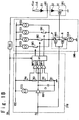
- FIG. 1B is a circuit diagram schematically showing a configuration example of the bus communication transceiver LTr in the first embodiment, and especially, the more detailed configuration of the delay time measurement circuit section DTM and the output waveform adjustment circuit section OWR.
- the components of the delay time measurement circuit section DTM and the output waveform adjustment circuit section OWR will be especially described.
- the bus communication transceiver LTr shown in FIG. 1B contains the transmission signal input node TX, the output waveform adjustment circuit section OWR, the bus connection node LBT, the output circuit section OPC, the reception circuit section RXC, the reception signal output node RX, the delay time measurement circuit section DTM, the slave resistance IsS, and the first diode D1.
- the output waveform adjustment circuit section OWR contains 0 th to fourth constant current sources ICC0 to ICC4, first to third switches SW1 to SW3, and an inverter INV1.
- the inverter INV is a so-called CMOS (Complementary Metal Oxide Semiconductor) type inverter which contains a P-channel type transistor P and an N-channel type transistor N.
- CMOS Complementary Metal Oxide Semiconductor
- the delay time measurement circuit section DTM contains a buffer BUF1, a capacitance C1, first to fourth resistances R1 to R4, first to third comparators CMP1 to CMP3 and a latch circuit section Lat.
- the output circuit section OPC contains the second diode D2 and the N-channel type transistor N1. Besides, the first power supply voltage VDD, the second power supply VSup and a ground voltage are further shown in FIG. 1B .
- the number of comparators CMP1 to CMP3 is 3, the number of switches SW1 to SW3 is 3, the number of resistances R1 to R4 is 4, and the number of constant current sources ICC0 to ICC5 is 6, but these numbers are an example only. That is, these numbers may be changed according to need and do not limit the configuration of the bus communication transceiver LTr in the present embodiment.
- the LIN is used as the bus LBS but this is an example only. That is, the bus communication transceiver in the present embodiment is applicable even in case of using a bus except the LIN.
- the kind of bus LBS is not limited in the present embodiment.
- the first power supply voltage VDD is connected with one of the ends of a fifth constant current source ICC5 and one of the ends of each of the 0 th to third constant current sources ICC0 to ICC3 in common.
- the other end of the first constant current source ICCl is connected with one of the ends of the first switch SW1.
- the other end of the second constant current source ICC2 is connected with one of the ends of the second switch SW2.
- the other end of the third constant current source ICC3 is connected with one of the ends of the third switch SW3.
- the other end of the 0th constant current source ICC0 and the other end of each of the first to third switches SW1 to SW3 are connected with the source of the P-channel type transistor P in common.
- the drain of the P-channel type transistor P and the drain of the N-channel type transistor N are connected with the gate of the N-channel type transistor N1 in common.
- the source of the N-channel type transistor N is connected with one of the ends of the fourth constant current source ICC4.
- the other end of the fourth constant current source ICC4 is grounded.
- a group of the 0 th to third constant current sources ICC0 to ICC3 and the first to third switches SW1 to SW3 is called a current source circuit section.
- the transmission signal input node TX is connected with the input node of the buffer BUF1, the gate of the P-channel type transistor P and the gate of the N-channel type transistor N in common.
- the output node of the buffer BUF1 is connected with one of the ends of the capacitance C1 and one of the input nodes of each of the first to third comparators CMP1 to CMP3 in common.
- the other end of the capacitance C1, one of the ends of the first resistance R1 and a negative supply supply node of the buffer BUF1 are grounded.
- the other end of the first resistance R1 is connected with the other input node of the first comparator CMP1 and one of the ends of the second resistance R2 in common.
- the other end of the second resistance R2 is connected with the other input node of the second comparator CMP2 and one of the ends of the third resistance R3 in common.
- the other end of the third resistance R3 is connected with the other input node of the third comparator CMP3 and one of the ends of the fourth resistance R4 in common.
- the other end of the fourth resistance R4 is connected with first power supply voltage VDD.
- a positive supply section of the buffer BUF1 is connected with the other end of the fifth constant current source ICC5.
- An output node of each of the first to third comparators CMP1 to CMP3 is connected with a corresponding one of first to third input nodes of the latch circuit section Lat.
- First to third output nodes of the latch circuit section Lat are connected with control signal input nodes of the first to third switches SW1 to SW3, respectively.
- An output node of the reception circuit section RXC is connected with the reception signal output node RX and a control signal input node of the latch circuit section Lat in common.
- the second power supply VSup is connected with one of the ends of the slave resistance IsS.
- the other end of the slave resistance IsS is connected with the anode of the first diode D1.
- the cathode of the first diode D is connected with the bus connection node LBT and an input node of the reception circuit section RXC and the anode of the second diode D2 in common.
- the cathode of the second diode D2 is connected with the drain of the N-channel type transistor N1.
- the source of the N-channel type transistor N1 is grounded.
- the buffer BUF1 outputs an output voltage after applying a voltage inclination according to the current supplied from the fifth constant current source ICC5 to the input signal.
- the signal voltage outputted from the buffer BUF1 is applied between both ends of the capacitance C1.
- the first to fourth resistances R1 to R4 are connected in series to divide a voltage between the first power supply voltage VDD and the ground voltage and generate the first to third reference voltages.
- the first to third comparators CMP1 to CMP3 compare a voltage applied to the capacitance C1 with the first to third reference voltages, and generate and output first to third comparison result signals showing the comparison results to the latch circuit section Lat, respectively.
- the latch circuit section Lat latches the first to third comparison result signals at a rising timing of a signal outputted from the reception circuit section RXC, and continues to output.
- the delay time measurement circuit section DTM in the first embodiment measures a time period from the rising time of the input signal supplied to the transmission signal input node TX to a rising time of the output signal generated from this input signal and outputted from the reception circuit section RXC, by measuring which of the first to third reference voltages the voltage of the capacitance C1 rises to.
- the rising signal waveform outputted from the output circuit section OPC to the bus connection node LBT based on the input signal receives dullness of waveform based on the capacitance C of the bus LBS and the second power supply VSup.
- a difference between the rising time (rising through rate) of an input signal and the rising time (rising through rate) of a rising signal at the bus connection node LBT can be reflected on a difference between a falling time (falling through rate) of the input signal and a falling time (falling through rate) of the falling signal in the bus connection node LBT
- the inventor thought of that the input signal can fall within a range by adjusting a duty ratio of the input signal.
- the delay time measurement circuit section DTM is an example to measure the difference between the rising time (rising through rate) of the input signal and the rising time (rising through rate) of the rising signal at the bus connection node LBT.
- the reflection on a difference between a falling time (falling through rate) of the input signal and a falling time (falling through rate) of the falling signal of the bus connection node LBT will be described later.
- the delay time is measured to express in four steps by using the three reference voltages. That is, the four steps for the voltage of the capacitance C1 are the 0 th step at which the voltage is less than the first reference voltage, the first step at which the voltage is equal to or more than the first reference voltage and less than the second reference voltage, the second step at which the voltage is equal to or more than the second reference voltage and less than the third reference voltage, and the third step at which the voltage is equal to or more than the third reference voltage.
- the first to third comparison result signals outputted from the first to third comparators CMP1 to CMP3 are used as a comparison result signal group showing these four steps (the 0 th to the third step).
- a comparison result signal group showing these four steps (the 0 th to the third step).
- the comparators if the voltage of the capacitance C1 is lower than the reference voltage of a corresponding number, a signal in a low state is outputted, and if being higher than it, a signal in a high state is outputted.
- all the comparison result signals are in the low state at the 0 th step, only the first comparison result signal is in the high state at the first step, only the first and second comparison result signals are in the high state at the second step, and all the comparison result signals are in the high state at the third step.
- the comparison result signal group showing these four steps is stored in the latch circuit section Lat and is transferred to the output waveform adjustment circuit section OWR as a delay time measurement result signal group.
- each of the 0 th to third constant current sources ICC0 to ICC3 supplies a constant current to the P-channel type transistor P of the first inverter INV1.
- the first to third switches SW1 to SW3 connect or disconnect the first to third constant current sources ICC1 to ICC3 and the first P-channel type transistor P of the inverter INV1 in response to the delay time measurement result signal group outputted from first to third latches L1 to L3 of the latch circuit section Lat, respectively.
- the first inverter INV1 changes a falling voltage waveform inclination of the transmission signal supplied from the transmission signal input node TX based on a total amount of current supplied from a part or entire of the 0 th to fourth constant current sources ICC0 to ICC4 and outputs to a gate of the transistor N1 of the output circuit section OPC.
- the drive ability of the transistor N1 (the falling voltage waveform inclination at the bus connection node LBT) is set based on the delay time measurement result at the time of rising of the input signal, and therefore, the falling time (the falling through rate) of the input signal is adjusted.
- the delay time measurement result signals with a high state set the switches SW1 to SW3 to the connection state and the delay time measurement result signals with a low state set the switches SW1 to SW3 to the disconnection state, as an example. That is, at the 0 th step, all of the first to third switches SW1 to SW3 are set to the disconnection state. At the first step, only the first switch SW1 is set to the connection state. At the second step, only the third switch SW3 is set to the disconnection state. At the third step, all the switches are set to the connection state.
- FIG. 1C is a block diagram schematically showing a configuration example of the latch circuit section Lat in the first embodiment. The components of the latch circuit section Lat in the first embodiment will be described.
- the latch circuit section Lat in the first embodiment contains first to the third latches L1 to L3. Note that although it is supposed that the number of latches L1 to L3 contained in the latch circuit section Lat is 3, the number is only made to correspond to the number of comparators CMP1 to CMP3 in the present embodiment, and does not limits the configuration of the latch circuit section Lat.
- the latch input nodes L1I to L3I of the first to third latches L1 to L3 are connected with the output nodes of the first to third comparator CMP1 to CMP3, respectively.
- the Latch output nodes L1O to L3O of the first to third latches L1 to L3 are connected with the control signal input nodes of the first to third switches SW1 to SW3, respectively.
- the control signal input nodes of the first to third latches L1 to L3 are connected with the output node of the reception circuit section RXC in common as a common control signal input node LC.
- Each of the first to third latches L1 to L3 latches the corresponding value of latch input node L1I to L3I at the rising edge of the control signal and continues to output a signal of the latched value until the next rising edge of the control signal LC.
- each of the first to third latches L1 to L3 may be further composed of a reset signal input node (not shown).
- a reset signal input node not shown.
- the latched values of the first to third latches L1 to L3 are overwritten in the bus communication transceiver LTr in the first embodiment, every time the output signal of the reception circuit section RXC rises, it does not need a reset signal basically.
- an ignition signal and a power on reset signal according to the start-up of an accessory power may be used as the reset signal.
- the values of the latch circuit section Lat upon resetting may be set to the center of all the steps (second step of four steps), the efficiency is good if the actual signal waveform is adjustable even though the through rate is larger or smaller.
- FIG. 2 is a time chart showing an example of the time change of a signal obtained from each section when the bus communication transceiver LTr in the first embodiment operates.
- the time chart shown in FIG. 2 contains first to fourth graphs (a) to (d).
- the first graph (a) shows a voltage change of the input signal supplied from the transmission signal input node TX of the bus communication transceiver LTr in accompaniment with elapse of the time.
- the second graph (b) shows a voltage change of the buffer signal outputted from the buffer BUF1 in accompaniment with elapse of the time.
- the third graph (c) shows a voltage change of a bus signal which the bus communication transceiver LTr inputs or outputs from or to the bus connection node LBT, in accompaniment with elapse of the time.
- the fourth graph (d) shows a voltage change of the output signal which the bus communication transceiver LTr outputs from the reception signal output node RX, in accompaniment with elapse of the time. It should be noted that in each of the first to fourth graphs (a) to (d), the horizontal axis shows an elapse of the time and the vertical axis shows the voltage change of each signal.
- the input signal shown in first graph (a) rises at the time t0 shown in FIG. 2 to switch from the low state to the high state.
- the buffer signal shown in second graph (b) is generated and the charging of the capacitance C1 is started with the voltage inclination determined based on the characteristic of the buffer BUF1, a current value of the fifth constant current source ICC5, and the capacitance value of the capacitance C and so on.
- This voltage inclination is mainly determined based on the current value of the fifth constant current source ICC5 and the capacitance value with the capacitance C1.
- the bus signal shown in third graph (c) starts rising in a waveform having the voltage inclination determined based on the second power supply VSup, the resistance value of the master resistance IsM of bus LBS and the capacitance value of the capacitance C1 coupled to the bus LBS mainly.
- the inverter INV1 there is a delay of the inverter INV1 and a delay not depending on the output waveform inclination of the output circuit section OPC. However, they are as small as it is possible to ignore on the time axis.
- the third graph (c) is a time when the signal intersects with a logical threshold value Vth of the reception circuit section RXC.
- the output signal shown in the fourth graph (d) rises at this time t1.
- the delay is as small as it is possible to ignore on the time axis. That is, the measured delay time becomes a time from the time t0 to the time t1 in FIG. 2 .
- the value of the comparison result of the voltage value of the second graph (b) at the time t1 with the reference voltages supplied to the comparators CMP1 to CMP3 is latched by the latch circuit section Lat.
- the latch circuit section Lat latches the state of the input signal at this time and, and continues to output it.
- the input signal shown in the first graph (a) falls down at the time t4 shown in FIG. 2 .
- the buffer signal shown in the second graph (b) falls down, to discharge the capacitance C1.
- the bus signal shown shown in the third graph (c) start falling in a waveform with the voltage inclination adjusted by the output waveform adjustment circuit section OWR.
- the output signal shown in the fourth graph (d) falls at the time t5 shown in FIG. 2 and the bus signal shown in the third graph (c) completes at a time t6.
- the time t5 is a time when the signal of the third graph (c) intersects with the logical threshold value Vth of the reception circuit section RXC.
- the falling waveform of the bus signal is adjusted by using the bus communication transceiver LTr in the first embodiment.
- FIG. 3A is a graph showing a waveform example of the bus signal when waveform adjustment is not carried out in the bus communication transceiver LTr in the first embodiment.
- FIG. 3B is s graph showing a waveform example of the bus signal when the voltage inclination at the time of falling of the bus signal shown in FIG. 3A is adjusted in the bus communication transceiver LTr in the first embodiment.
- the horizontal axis shows elapse of time t and the vertical axis shows the voltage VLBs of the bus signal, in FIG. 3A and FIG. 3B .
- the measured delay time is shorter than a preset value (an initial value or a value latched in the latch circuit section Lat).
- the voltage inclination G1 at the time of falling of the bus signal is adjusted to a steeper voltage inclination G2, i.e. the through rate of the falling waveform rate is made larger.
- FIG. 3C is a graph showing another waveform example of the bus signal when the waveform adjustment is not carried out in the bus communication transceiver LTr in the first embodiment.
- FIG. 3D is a graph showing a waveform example of the bus signal when the voltage inclination at the time of falling of the bus signal shown in Fig. 3C is adjusted in the bus communication transceiver LTr in the first embodiment.
- the horizontal axis shows the elapse of time t and the vertical axis shows the voltage VLBs of the bus signal, in FIG. 3C and FIG. 3D .
- the measured delay time is longer than the preset value (initial value or value latched by the latch circuit section Lat).
- the voltage inclination G3 at the time of falling of the bus signal is adjusted to a gentle voltage inclination G4, i.e. it is made smaller than the falling waveform through rate.
- a waveform duty (a high level period) is defined by using the time D1 and the time D2 shown in FIG. 3A to FIG. 3D .
- the time D1 is defined as a time period from the time t2 at which the bus signal rises and reaches a predetermined voltage to the time t3 at which the bus signal falls and reaches a predetermined voltage.
- the time D2 is defined as a time period from the time t1 at which the bus signal rises and reaches a predetermined voltage to the time t4 at which the bus signal falls and reaches a predetermined voltage.
- the bus communication transceiver in the first embodiment it is possible to apply an appropriate voltage inclination to the falling waveform of the bus signal for every measurement results of delay time, by suitably setting the characteristics of the buffer BUF1, the current quantities of the 0th to fifth constant current sources ICC0 to ICC5, the resistance values of the first to fourth resistances R1 to R4, and the capacitance value of the capacitanceCl, and so on in advance based on such definitions.
- the bus signal not to come off the range defined in the LIN standard and so on.
- the time period from the time t0 (the rising of the input signal supplied from the transmission signal input node TX) to the time t4 (the falling of the input signal supplied from the transmission signal input node TX) is generally equal to the time period from the time t4 to the next rising of the input signal supplied from the transmission signal input node TX.
- the duty at this time is called the duty ratio of 50%.
- a time period while the voltage of the bus signal (waveform shown in the graph (c)) is higher than a logical threshold value Vth is a high level time
- a time period while the voltage of the bus signal is lower than the logical threshold value Vth is a low level time.
- the high level time and the low level time are repeated in a time T
- the high level time becomes longer than the low level time when the falling time is longer than the rising time as shown in FIG. 3A .
- the high level time becomes shorter than the low level time when the falling time is shorter than the rising time.
- the high level time and the low level time of the bus signal are made equal to each other by adjusting that the rising time and the falling time are made equal to each other, in the bus communication transceiver in the first embodiment.
- a processing possible time of the high level signal and a process possible time of the low level signal can be made maximum.
- the effect can be indicated in the speed-up of the signal and the stabilization of taking-in of the signal.
- FIG. 4 is a circuit diagram schematically showing the configuration of the bus communication transceiver LTr in a second embodiment, especially, the delay time measurement circuit section DTM and the output waveform adjustment circuit section OWR. It should be noted that because the overall configuration of the bus communication transceiver Ltr and the bus LBS in the second embodiment is the same as that of the first embodiment shown in FIG. 1A , the description is omitted.
- the configuration of the bus communication transceiver LTr in the second embodiment shown in FIG. 4 is almost the same as the configuration of the bus communication transceiver LTr in the first embodiment shown in FIG. 1B and different points will be described below. That is, the bus communication transceiver LTr in the second embodiment is the same as the configuration formed by adding the second inverter INV2 and the fourth switch SW4 to the bus communication transceiver LTr in the first embodiment.
- bus communication transceiver LTr in the second embodiment are the same as those of the bus communication transceiver LTr in the first embodiment, a further detailed description is omitted.
- the connection relation according to the second inverter INV2 and the fourth switch SW4 will be described.
- the input node of the second inverter INV2 is connected with the transmission signal input node TX.
- the output node of the second inverter INV2 is connected with the control signal input node of the fourth switch SW4.
- One of the ends of the fourth switch SW4 is connected with the first power supply voltage VDD.
- the other end of the fourth switch SW4 is connected with the other end of the fourth resistance R4.
- the second inverter INV2 outputs an output signal in a high state when the transmission signal supplied from the transmission signal input node TX is in the low state.
- the second inverter INV2 outputs the output signal in the low state when the transmission signal supplied from the transmission signal input node TX is in the high state.
- the fourth switch SW4 is set to a blocking-off state when the output signal of the second inverter INV2 is in the high state and set to a conductive state when the output signal of the second inverter INV2 is in the low state.
- bus communication transceiver LTr in the second embodiment is the same as that of the bus communication transceiver LTr in the first embodiment, further detailed description is omitted.
- the effect of the second embodiment is in that the output waveform adjustment circuit section OWR does not carry out a waveform adjustment and the consumed power due to the current flowing through the first to fourth resistances R1 to R4 can be saved when the transmission signal is in the low state. Therefore, another configuration may be applied as far as it fits with this purpose, of course.
- FIG. 5 is a circuit diagram schematically showing the configuration of the bus communication transceiver LTr in a third embodiment, especially, the delay time measurement circuit section DTM and the output waveform adjustment circuit section OWR. It should be noted that because the overall configuration of the bus communication transceiver Ltr and the bus LBS in the second embodiment is the same as that of the first embodiment shown in FIG. 1A , the description is omitted.
- the configuration of the bus communication transceiver LTr in the second embodiment shown in FIG. 5 is almost the same as that of the bus communication transceiver LTr in the first embodiment shown in FIG. 1B other than the configuration of the delay time measurement circuit section DTM.
- the components of the delay time measurement circuit section DTM in the third embodiment will be described.
- the delay time measurement circuit section DTM in the third embodiment contains first to third buffers BUF1 to BUF3, first to third capacitances C1 to C3, the first to third comparators CMP1 to CMP3, the latch circuit section Lat, the first and second resistances R1 and R2, fifth to seventh constant current sources ICC5 to ICC7, the second inverter INV1, and the fourth switch SW4.
- bus communication transceiver LTr in the third embodiment are the same as those of the first or second embodiment, a further detailed description is omitted.
- each of the fifth to seventh constant current sources ICC5 to ICC7 is connected with the first power supply voltage VDD.
- the other end of each of the fifth to seventh constant current sources ICC5 to ICC7 is connected with one of power supply sections of corresponding one of the first to third buffers BUF1 to BUF3.
- the other power supply section of each of the first to third buffers BUF1 to BUF3 is grounded.
- Input nodes of the first to third buffers BUF1 to BUF3 and the input node of the second inverter INV2 are connected with the transmission signal input node TX in common.
- An output node of each of the first to third the buffers BUF1 to BUF3 is connected with one of the input nodes of each of the first to third comparators CMP1 to CMP3. Moreover, an output node of each of the first to third buffers BUF1 to BUF3 is connected with one of the ends of a corresponding one of the first to third capacitances C1 to C3. The other end of each of the first to third capacitances C1 to C3 is grounded.
- the output node of the second inverter INV2 is connected with the control signal input node of the fourth switch SW4. One of the ends of the fourth switch SW4 is connected with the first power supply voltage VDD. One of the ends of the first resistance R1 is grounded.
- the other end of the first resistance R1 is connected with one of the ends of the second resistance R2 and the other input node of each of the first to third comparators CMP1 to CMP3 in common.
- the other end of the second resistance R2 is connected with the other end of the fourth switch SW4.
- An output node of each of the first to third comparators CMP1 to CMP3 is connected with a corresponding one of the first to third input nodes of the latch circuit section Lat.
- a control signal input node of the latch circuit section Lat is connected with the output node of the reception circuit section RXC.
- the first to third output nodes of the latch circuit section Lat are connected with the control signal input nodes of the first to third switches SW1 to SW3, respectively.
- the first to third buffers BUF1 to BUF3 output signals obtained by applying voltage inclinations according to the currents supplied from the fifth to seventh constant current sources to the input signal, respectively.
- the voltage of the signal outputted from each of the first to third buffers BUF1 to BUF3 is applied to one end of a corresponding one of the first to third capacitances C1 to C3.
- the fourth switch SW4 is set to the conductive state, the first and the second resistances R1 and R2 generates a reference voltage by dividing the voltage between the first power supply voltage VDD and the ground voltage.
- the first to third comparators CMP1 to CMP3 compares the voltages applied to the first to third capacitances C1 to C3 with the reference voltage, and generates and outputs first to third comparison result signals showing the comparison results to the latch circuit section Lat.
- the latch circuit section Lat latches the first to third comparison result signals when the signal outputted from the reception circuit section RXC rises and continues to output the latched signal.
- bus communication transceiver LTr in the third embodiment is the same as that of the first or second embodiment, a further detailed description is omitted.
- the second inverter INV2 and the fourth switch SW4 provided in the bus communication transceiver LTr in the third embodiment are possible to be replaced with other components, like the second embodiment shown in FIG. 4 . Moreover, they may be omitted like the first embodiment shown in FIG. 1B .
- the present invention made by the inventor has been specifically described based on the embodiments. However, the present invention is not limited to the embodiments, and various modifications are possible in a range which does not deviate from the technical range of the present invention. Especially, the bus communication transceiver which fits with the LIN standard has been described. However, the present invention can be applied to another configuration using a single wire bus.
- the single wire bus means a bus configuration in which a plurality of input nodes, output nodes, and bidirectional nodes are connected with a common one signal line (or one set of signal lines).
- the signal line may be a single line on which a single end signal is transferred, or two signal lines may transfer a set of complementary signals.
- the embodiments may be freely combined in a range in which there is no contradiction.
- a bus communication transceiver measures a delay time in response to a rising time of a signal and adjusts a falling waveform of the same signal based on the measurement result.
- a signal waveform, especially, a duty ratio can be adjusted in a predetermined standard range.
- the bus communication transceiver realizes an excellent real-time operation, without receiving influence of a variation of the voltage supplied to the bus, and a variation of a total of loads connected with the bus.
- the bus communication transceiver measures the delay time by using the signal and adjusts the waveform of the signal.
Landscapes
- Engineering & Computer Science (AREA)
- Computer Networks & Wireless Communication (AREA)
- Signal Processing (AREA)
- Power Engineering (AREA)
- Dc Digital Transmission (AREA)
- Logic Circuits (AREA)
- Small-Scale Networks (AREA)
Claims (7)
- Buskommunikations-Transceiver (LTr), umfassend:einen Eingangsknoten (TX), der konfiguriert ist, um ein Eingangssignal zu empfangen;eine Sendeschaltung (TXC), die konfiguriert ist, um das Eingangssignal vom Eingangsknoten (TX) zu empfangen und ein Sendesignal zu erzeugen;einen Busverbindungsknoten (LBT), der mit einem externen Einzeldrahtbus (LBS) verbunden ist, um das Sendesignal zum externen Einzeldrahtbus (LBS) zu senden und ein Empfangssignal vom externen Einzeldrahtbus (LBS) zu empfangen;eine Empfangsschaltung (RXC), die konfiguriert ist, um das Empfangssignal oder das Sendesignal vom Einzeldrahtbus (LBS) zu empfangen, um ein Ausgangssignal zu erzeugen; undeinen Ausgangsknoten (RX), der konfiguriert ist, um das Ausgangssignal auszugeben;gekennzeichnet durcheine Verzögerungszeit-Messschaltung (DTM), die konfiguriert ist, um eine Verzögerungszeit zwischen einer ansteigenden Wellenform eines zum Eingangsknoten (TX) zugeführten Eingangssignals und einer ansteigenden Wellenform eines auf einer Basis des den Ausgangsknoten (RX) erreichenden zugeführten Eingangssignals erzeugten Ausgangssignals zu messen und eine Verzögerungszeit-Messergebnissignalgruppe zu erzeugen, die die Messergebnisse zeigt,wobei die Sendeschaltung (TXC) eine Ausgangswellenform-Einstellschaltung (OWR) umfasst, die konfiguriert ist, um eine Spannungsneigung in einer abfallenden Wellenform des aus dem Ausgangssignal erzeugten Sendesignals basierend auf der Verzögerungszeit-Messergebnissignalgruppe zu einzustellen,wobei die Ausgangswellenform-Einstellschaltung (OWR) folgendes umfasst:eine Stromquellenschaltung, die konfiguriert ist, um Ströme mit unterschiedlichen Stromwerten basierend auf der Verzögerungszeit-Messergebnissignalgruppe zuzuführen; undeine Inverterschaltung (INV1), die konfiguriert ist, um das Eingangssignal zu empfangen und Zwischensignale auszugeben, die unterschiedliche Spannungsneigungen haben, und zwar basierend auf den von der Stromquellenschaltung zugeführten Strömen,wobei die Sendeschaltung (TXC) weiterhin folgendes umfasst:
eine Ausgangsschaltung (OPC), die konfiguriert ist, um das Sendesignal aus den Zwischensignalen zu erzeugen. - Buskommunikations-Transceiver (LTr) nach Anspruch 1, wobei die Stromquellenschaltung folgendes umfasst:eine Hauptstromquelle (ICCO), die konfiguriert ist, um einen Hauptstrom zur Inverterschaltung (INV1) zuzuführen;eine Vielzahl von Unterstromquellen (ICC1 bis ICC3), die konfiguriert sind, um jeweils eine Vielzahl von Unterströmen zur Inverterschaltung (INV1) zuzuführen;eine Vielzahl von Schaltern (SW1 bis SW3), die mit der Vielzahl von Unterstromquellen (ICC1 bis ICC3) in Reihe geschaltet sind, um eine Schaltoperation auszuführen, um Zustände zwischen einem Teil oder einer Gesamtheit der Vielzahl von Unterströmen und der Inverterschaltung (INV1) auf leitende Zustände oder absperrende Zustände einzustellen.
- Buskommunikations-Transceiver (LTr) nach Anspruch 2, wobei die Verzögerungszeit-Messschaltung (DTM) folgendes umfasst:eine Puffer-Konstantstromquelle (ICC5), die konfiguriert ist, um einen Pufferstrom zuzuführen;einen Puffer (BUF1), der konfiguriert ist, um das Eingangssignal zu empfangen und die Spannungsneigung auszugeben, und zwar basierend auf dem Pufferstrom (ICC5);eine Kapazität (C1), die mit einem Ausgangsknoten des Puffers (BUF1) verbunden ist;eine Vielzahl von Widerständen (R1 bis R4), die zwischen einer ersten Energieversorgungsspannung (VDD) und einer zweiten Energieversorgungsspannung (Vsup) in Reihe geschaltet sind, um eine Vielzahl von durch Teilen einer Spannung zwischen der ersten Energieversorgungsspannung (VDD) und der zweiten Energieversorgungsspannung (Vsup) erzeugten Referenzspannungen zu erzeugen;eine Vielzahl von Komparatoren (CMP1 bis CMP3), die konfiguriert sind, um eine an die Kapazität (C1) angelegte Spannung mit der Vielzahl von Referenzspannungen zu vergleichen, um die Vergleichsergebnissignalgruppe auszugeben, die die Vergleichsergebnisse anzeigt; undeine Latch-Schaltung (Lat), die konfiguriert ist, um die Vergleichsergebnissignalgruppe zu einer Zeit eines Ansteigens des Ausgangssignals zwischenzuspeichern, um die zwischengespeicherten Signale als die Verzögerungszeit-Messergebnissignalgruppe auszugeben.
- Buskommunikations-Transceiver (LTr) nach Anspruch 2, wobei die Verzögerungszeit-Messschaltung (DTM) folgendes umfasst:eine Vielzahl von Puffer-Konstantstromquellen (ICC5 bis ICC7), um eine Vielzahl von Pufferströmen zuzuführen;eine Vielzahl von Puffern (BUF1 bis BUF3), die konfiguriert sind, um das Eingangssignal zu empfangen und eine Vielzahl von Spannungsneigungen jeweils entsprechend der Vielzahl von Pufferströmen auszugeben;eine Vielzahl von Kapazitäten (C1 bis C3), die jeweils mit Ausgangsknoten der Vielzahl von Puffern (BUF1 bis BUF3) verbunden sind;eine Vielzahl von Widerständen (R1 und R2), die zwischen einer ersten Energieversorgungsspannung (VDD) und einer zweiten Energieversorgungsspannung (Vsup) in Reihe geschaltet sind, um durch Teilen einer Spannung zwischen der Energieversorgungsspannung (VDD) und der zweiten Energieversorgungsspannung (Vsup) Referenzspannungen zu erzeugen;eine Vielzahl von Komparatoren (CMP1 bis CMP3), die konfiguriert sind, um an die Vielzahl der Kapazitäten (C1 bis C3) angelegte Spannungen jeweils mit den Referenzspannungen zu vergleichen und um eine Vergleichsergebnissignalgruppe auszugeben, die Vergleichsergebnisse zeigt; undeine Latch-Schaltung (Lat), die konfiguriert ist, um die Vergleichsergebnissignalgruppe in Antwort auf eine Anstiegszeit des Ausgangssignals zwischenzuspeichern, um sie als eine Verzögerungszeit-Messergebnissignalgruppe auszugeben.
- Buskommunikations-Transceiver (LTr) nach Anspruch 3 oder 4, wobei die Latch-Schaltung (Lat) folgendes umfasst:
eine Vielzahl von Zwischenspeichern (L1 bis L3) mit Eingangsknoten, die mit Ausgangsknoten der Vielzahl von Komparatoren (CMP1 bis CMP3) verbunden sind, und mit Ausgangsknoten, die jeweils mit Steuersignal-Eingangsknoten der Vielzahl von Schaltern (SW1 bis SW3) verbunden sind. - Buskommunikations-Transceiver (LTr) nach Anspruch 3 oder 4, der weiterhin folgendes umfasst:
einen Schalter (SW4), der konfiguriert ist, um die Vielzahl von Widerständen (R1 bis R4; R1 und R2) mit der ersten oder zweiten Energieversorgungsspannung (VDD; Vsup) während einer Messung der Verzögerungszeit zu verbinden und um die Vielzahl von Widerständen (R1 bis R4; R1 und R2) von der ersten oder zweiten Energieversorgungsspannung (VDD; Vsup) während einem Teil oder einer Gesamtheit einer Zeitperiode zu trennen, für welche die Messung der Verzögerungszeit unnötig ist. - Buskommunikations-Transceiver (LTr) nach Anspruch 5, der weiterhin folgendes umfasst:
einen Schalter (SW4), der konfiguriert ist, um die Vielzahl von Widerständen (R1 bis R4; R1 und R2) mit der ersten oder zweiten Energieversorgungsspannung (VDD; Vsup) während einer Messung der Verzögerungszeit zu verbinden und um die Vielzahl von Widerständen (R1 bis R4; R1 und R2) von der ersten oder zweiten Energieversorgungsspannung (VDD; Vsup) während einem Teil oder einer Gesamtheit einer Zeitperiode zu trennen, für welche die Messung der Verzögerungszeit unnötig ist.
Applications Claiming Priority (1)
| Application Number | Priority Date | Filing Date | Title |
|---|---|---|---|
| JP2013019968A JP6013214B2 (ja) | 2013-02-04 | 2013-02-04 | バス通信トランシーバ |
Publications (3)
| Publication Number | Publication Date |
|---|---|
| EP2765745A2 EP2765745A2 (de) | 2014-08-13 |
| EP2765745A3 EP2765745A3 (de) | 2014-10-01 |
| EP2765745B1 true EP2765745B1 (de) | 2018-09-19 |
Family
ID=50071432
Family Applications (1)
| Application Number | Title | Priority Date | Filing Date |
|---|---|---|---|
| EP14153770.4A Active EP2765745B1 (de) | 2013-02-04 | 2014-02-04 | Bus-Kommunikationssendeempfänger |
Country Status (4)
| Country | Link |
|---|---|
| US (2) | US9014242B2 (de) |
| EP (1) | EP2765745B1 (de) |
| JP (1) | JP6013214B2 (de) |
| CN (1) | CN103973279B (de) |
Families Citing this family (5)
| Publication number | Priority date | Publication date | Assignee | Title |
|---|---|---|---|---|
| JP2017200103A (ja) * | 2016-04-28 | 2017-11-02 | ローム株式会社 | 信号処理装置及びバス通信システム |
| US10120434B2 (en) * | 2016-05-13 | 2018-11-06 | Infineon Technologies Ag | Semiconductor device chip package with electronic switching using dedicated ground pin coupled to a virtual ground node |
| CN106911334B (zh) * | 2017-02-28 | 2021-08-10 | 光和电科技(广东)有限公司 | 一种消防工业总线编码方法 |
| JP7331756B2 (ja) * | 2020-03-30 | 2023-08-23 | 株式会社デンソー | 通信装置 |
| US12562633B2 (en) * | 2022-11-10 | 2026-02-24 | Qorvo Us, Inc. | Using different voltage levels to close a switch in a switch converter |
Family Cites Families (13)
| Publication number | Priority date | Publication date | Assignee | Title |
|---|---|---|---|---|
| JP3410547B2 (ja) * | 1994-05-24 | 2003-05-26 | 三菱電機株式会社 | 半導体装置の出力回路 |
| US5936520A (en) * | 1997-11-13 | 1999-08-10 | Chrysler Corporation | Analog sensor status detection single wire bus multiplex system |
| JP2001274670A (ja) | 2000-03-27 | 2001-10-05 | Toshiba Corp | Lsiの出力回路 |
| JP3522668B2 (ja) * | 2000-08-10 | 2004-04-26 | ローム株式会社 | 信号伝達装置 |
| US6366115B1 (en) * | 2001-02-21 | 2002-04-02 | Analog Devices, Inc. | Buffer circuit with rising and falling edge propagation delay correction and method |
| JP2004320530A (ja) * | 2003-04-17 | 2004-11-11 | Ricoh Co Ltd | 電源供給システム装置 |
| JP2004336654A (ja) * | 2003-05-12 | 2004-11-25 | Fujitsu Ltd | 出力インターフェイス回路及び半導体装置 |
| US7672363B2 (en) * | 2004-05-27 | 2010-03-02 | Tag Safety Systems, Inc. | Method of and system for determining the delay of digital signals |
| US7230464B2 (en) * | 2004-06-29 | 2007-06-12 | Intel Corporation | Closed-loop delay compensation for driver |
| US7768296B2 (en) * | 2006-02-23 | 2010-08-03 | Freescale Semiconductor, Inc. | Electronic device and method |
| JP4988417B2 (ja) * | 2007-04-20 | 2012-08-01 | ルネサスエレクトロニクス株式会社 | 出力回路 |
| JP5012414B2 (ja) * | 2007-10-26 | 2012-08-29 | 株式会社デンソー | ドライブ回路 |
| JP5491969B2 (ja) * | 2010-05-31 | 2014-05-14 | ローム株式会社 | トランスミッタ、インタフェイス装置、車載通信システム |
-
2013
- 2013-02-04 JP JP2013019968A patent/JP6013214B2/ja not_active Expired - Fee Related
-
2014
- 2014-01-30 US US14/168,968 patent/US9014242B2/en active Active
- 2014-02-04 EP EP14153770.4A patent/EP2765745B1/de active Active
- 2014-02-07 CN CN201410045102.5A patent/CN103973279B/zh active Active
-
2015
- 2015-04-20 US US14/690,983 patent/US9252984B2/en active Active
Non-Patent Citations (1)
| Title |
|---|
| None * |
Also Published As
| Publication number | Publication date |
|---|---|
| JP2014154894A (ja) | 2014-08-25 |
| CN103973279A (zh) | 2014-08-06 |
| EP2765745A3 (de) | 2014-10-01 |
| EP2765745A2 (de) | 2014-08-13 |
| US20140219323A1 (en) | 2014-08-07 |
| US9014242B2 (en) | 2015-04-21 |
| JP6013214B2 (ja) | 2016-10-25 |
| US9252984B2 (en) | 2016-02-02 |
| CN103973279B (zh) | 2018-05-11 |
| US20150229494A1 (en) | 2015-08-13 |
Similar Documents
| Publication | Publication Date | Title |
|---|---|---|
| US8766647B2 (en) | Method and apparatus for power sequence timing to mitigate supply resonance in power distribution network | |
| EP2765745B1 (de) | Bus-Kommunikationssendeempfänger | |
| US9866215B2 (en) | High speed low current voltage comparator | |
| US20140085123A1 (en) | Apparatus, system, and method for voltage swing and duty cycle adjustment | |
| CN101231626A (zh) | 接口电路和半导体集成电路 | |
| US20110115526A1 (en) | Microcomputer, Hysteresis comparator circuit, and voltage monitoring apparatus | |
| US7940102B2 (en) | Edge rate control for I2C bus applications | |
| JP2010166108A (ja) | 遅延回路 | |
| JP2014230091A (ja) | 抵抗調整回路、及び、抵抗調整方法 | |
| US8040160B2 (en) | Driver arrangement and signal generation method | |
| US7737748B2 (en) | Level shifter of semiconductor device and method for controlling duty ratio in the device | |
| US7187197B2 (en) | Transmission line driver | |
| US20050089106A1 (en) | Data transmission system and method | |
| US7965209B2 (en) | A/D conversion circuit and A/D conversion method | |
| US8575967B2 (en) | Smart edge detector | |
| US7902893B1 (en) | Clock-signal generator | |
| US20220085810A1 (en) | Driver for a shared bus, in particular a lin bus | |
| CN121233515B (zh) | 单线总线信号的接收电路以及接收方法 | |
| US20130135037A1 (en) | Voltage multiplying circuit, signal switch chip and impedance adjusting method thereof | |
| EP2124338B1 (de) | Taktsignalerzeuger | |
| US20220334998A1 (en) | Method and device for operating a transfer device | |
| US8019033B2 (en) | Data transmission system, controller, and its method | |
| JP2025050582A (ja) | 送信回路、電子制御ユニット、及び車両 | |
| JP4954257B2 (ja) | 伝送回路、cmos半導体デバイス、及び設計方法 |
Legal Events
| Date | Code | Title | Description |
|---|---|---|---|
| PUAI | Public reference made under article 153(3) epc to a published international application that has entered the european phase |
Free format text: ORIGINAL CODE: 0009012 |
|
| 17P | Request for examination filed |
Effective date: 20140204 |
|
| AK | Designated contracting states |
Kind code of ref document: A2 Designated state(s): AL AT BE BG CH CY CZ DE DK EE ES FI FR GB GR HR HU IE IS IT LI LT LU LV MC MK MT NL NO PL PT RO RS SE SI SK SM TR |
|
| AX | Request for extension of the european patent |
Extension state: BA ME |
|
| RIC1 | Information provided on ipc code assigned before grant |
Ipc: H04L 25/02 20060101AFI20140722BHEP |
|
| PUAL | Search report despatched |
Free format text: ORIGINAL CODE: 0009013 |
|
| AK | Designated contracting states |
Kind code of ref document: A3 Designated state(s): AL AT BE BG CH CY CZ DE DK EE ES FI FR GB GR HR HU IE IS IT LI LT LU LV MC MK MT NL NO PL PT RO RS SE SI SK SM TR |
|
| AX | Request for extension of the european patent |
Extension state: BA ME |
|
| RIC1 | Information provided on ipc code assigned before grant |
Ipc: H04L 25/02 20060101AFI20140825BHEP |
|
| R17P | Request for examination filed (corrected) |
Effective date: 20150401 |
|
| RBV | Designated contracting states (corrected) |
Designated state(s): AL AT BE BG CH CY CZ DE DK EE ES FI FR GB GR HR HU IE IS IT LI LT LU LV MC MK MT NL NO PL PT RO RS SE SI SK SM TR |
|
| RAP1 | Party data changed (applicant data changed or rights of an application transferred) |
Owner name: RENESAS ELECTRONICS CORPORATION |
|
| GRAP | Despatch of communication of intention to grant a patent |
Free format text: ORIGINAL CODE: EPIDOSNIGR1 |
|
| STAA | Information on the status of an ep patent application or granted ep patent |
Free format text: STATUS: GRANT OF PATENT IS INTENDED |
|
| INTG | Intention to grant announced |
Effective date: 20180423 |
|
| RIN1 | Information on inventor provided before grant (corrected) |
Inventor name: KIUCHI, HIDEKI |
|
| GRAS | Grant fee paid |
Free format text: ORIGINAL CODE: EPIDOSNIGR3 |
|
| GRAA | (expected) grant |
Free format text: ORIGINAL CODE: 0009210 |
|
| STAA | Information on the status of an ep patent application or granted ep patent |
Free format text: STATUS: THE PATENT HAS BEEN GRANTED |
|
| AK | Designated contracting states |
Kind code of ref document: B1 Designated state(s): AL AT BE BG CH CY CZ DE DK EE ES FI FR GB GR HR HU IE IS IT LI LT LU LV MC MK MT NL NO PL PT RO RS SE SI SK SM TR |
|
| REG | Reference to a national code |
Ref country code: GB Ref legal event code: FG4D |
|
| REG | Reference to a national code |
Ref country code: CH Ref legal event code: EP |
|
| REG | Reference to a national code |
Ref country code: AT Ref legal event code: REF Ref document number: 1044567 Country of ref document: AT Kind code of ref document: T Effective date: 20181015 |
|
| REG | Reference to a national code |
Ref country code: IE Ref legal event code: FG4D |
|
| REG | Reference to a national code |
Ref country code: DE Ref legal event code: R096 Ref document number: 602014032402 Country of ref document: DE |
|
| REG | Reference to a national code |
Ref country code: NL Ref legal event code: MP Effective date: 20180919 |
|
| PG25 | Lapsed in a contracting state [announced via postgrant information from national office to epo] |
Ref country code: GR Free format text: LAPSE BECAUSE OF FAILURE TO SUBMIT A TRANSLATION OF THE DESCRIPTION OR TO PAY THE FEE WITHIN THE PRESCRIBED TIME-LIMIT Effective date: 20181220 Ref country code: LT Free format text: LAPSE BECAUSE OF FAILURE TO SUBMIT A TRANSLATION OF THE DESCRIPTION OR TO PAY THE FEE WITHIN THE PRESCRIBED TIME-LIMIT Effective date: 20180919 Ref country code: BG Free format text: LAPSE BECAUSE OF FAILURE TO SUBMIT A TRANSLATION OF THE DESCRIPTION OR TO PAY THE FEE WITHIN THE PRESCRIBED TIME-LIMIT Effective date: 20181219 Ref country code: RS Free format text: LAPSE BECAUSE OF FAILURE TO SUBMIT A TRANSLATION OF THE DESCRIPTION OR TO PAY THE FEE WITHIN THE PRESCRIBED TIME-LIMIT Effective date: 20180919 Ref country code: NO Free format text: LAPSE BECAUSE OF FAILURE TO SUBMIT A TRANSLATION OF THE DESCRIPTION OR TO PAY THE FEE WITHIN THE PRESCRIBED TIME-LIMIT Effective date: 20181219 Ref country code: FI Free format text: LAPSE BECAUSE OF FAILURE TO SUBMIT A TRANSLATION OF THE DESCRIPTION OR TO PAY THE FEE WITHIN THE PRESCRIBED TIME-LIMIT Effective date: 20180919 Ref country code: SE Free format text: LAPSE BECAUSE OF FAILURE TO SUBMIT A TRANSLATION OF THE DESCRIPTION OR TO PAY THE FEE WITHIN THE PRESCRIBED TIME-LIMIT Effective date: 20180919 |
|
| REG | Reference to a national code |
Ref country code: LT Ref legal event code: MG4D |
|
| PG25 | Lapsed in a contracting state [announced via postgrant information from national office to epo] |
Ref country code: LV Free format text: LAPSE BECAUSE OF FAILURE TO SUBMIT A TRANSLATION OF THE DESCRIPTION OR TO PAY THE FEE WITHIN THE PRESCRIBED TIME-LIMIT Effective date: 20180919 Ref country code: AL Free format text: LAPSE BECAUSE OF FAILURE TO SUBMIT A TRANSLATION OF THE DESCRIPTION OR TO PAY THE FEE WITHIN THE PRESCRIBED TIME-LIMIT Effective date: 20180919 Ref country code: HR Free format text: LAPSE BECAUSE OF FAILURE TO SUBMIT A TRANSLATION OF THE DESCRIPTION OR TO PAY THE FEE WITHIN THE PRESCRIBED TIME-LIMIT Effective date: 20180919 |
|
| REG | Reference to a national code |
Ref country code: AT Ref legal event code: MK05 Ref document number: 1044567 Country of ref document: AT Kind code of ref document: T Effective date: 20180919 |
|
| PG25 | Lapsed in a contracting state [announced via postgrant information from national office to epo] |
Ref country code: IS Free format text: LAPSE BECAUSE OF FAILURE TO SUBMIT A TRANSLATION OF THE DESCRIPTION OR TO PAY THE FEE WITHIN THE PRESCRIBED TIME-LIMIT Effective date: 20190119 Ref country code: AT Free format text: LAPSE BECAUSE OF FAILURE TO SUBMIT A TRANSLATION OF THE DESCRIPTION OR TO PAY THE FEE WITHIN THE PRESCRIBED TIME-LIMIT Effective date: 20180919 Ref country code: EE Free format text: LAPSE BECAUSE OF FAILURE TO SUBMIT A TRANSLATION OF THE DESCRIPTION OR TO PAY THE FEE WITHIN THE PRESCRIBED TIME-LIMIT Effective date: 20180919 Ref country code: RO Free format text: LAPSE BECAUSE OF FAILURE TO SUBMIT A TRANSLATION OF THE DESCRIPTION OR TO PAY THE FEE WITHIN THE PRESCRIBED TIME-LIMIT Effective date: 20180919 Ref country code: IT Free format text: LAPSE BECAUSE OF FAILURE TO SUBMIT A TRANSLATION OF THE DESCRIPTION OR TO PAY THE FEE WITHIN THE PRESCRIBED TIME-LIMIT Effective date: 20180919 Ref country code: PL Free format text: LAPSE BECAUSE OF FAILURE TO SUBMIT A TRANSLATION OF THE DESCRIPTION OR TO PAY THE FEE WITHIN THE PRESCRIBED TIME-LIMIT Effective date: 20180919 Ref country code: NL Free format text: LAPSE BECAUSE OF FAILURE TO SUBMIT A TRANSLATION OF THE DESCRIPTION OR TO PAY THE FEE WITHIN THE PRESCRIBED TIME-LIMIT Effective date: 20180919 Ref country code: CZ Free format text: LAPSE BECAUSE OF FAILURE TO SUBMIT A TRANSLATION OF THE DESCRIPTION OR TO PAY THE FEE WITHIN THE PRESCRIBED TIME-LIMIT Effective date: 20180919 Ref country code: ES Free format text: LAPSE BECAUSE OF FAILURE TO SUBMIT A TRANSLATION OF THE DESCRIPTION OR TO PAY THE FEE WITHIN THE PRESCRIBED TIME-LIMIT Effective date: 20180919 |
|
| PG25 | Lapsed in a contracting state [announced via postgrant information from national office to epo] |
Ref country code: PT Free format text: LAPSE BECAUSE OF FAILURE TO SUBMIT A TRANSLATION OF THE DESCRIPTION OR TO PAY THE FEE WITHIN THE PRESCRIBED TIME-LIMIT Effective date: 20190119 Ref country code: SM Free format text: LAPSE BECAUSE OF FAILURE TO SUBMIT A TRANSLATION OF THE DESCRIPTION OR TO PAY THE FEE WITHIN THE PRESCRIBED TIME-LIMIT Effective date: 20180919 Ref country code: SK Free format text: LAPSE BECAUSE OF FAILURE TO SUBMIT A TRANSLATION OF THE DESCRIPTION OR TO PAY THE FEE WITHIN THE PRESCRIBED TIME-LIMIT Effective date: 20180919 |
|
| REG | Reference to a national code |
Ref country code: DE Ref legal event code: R097 Ref document number: 602014032402 Country of ref document: DE |
|
| PLBE | No opposition filed within time limit |
Free format text: ORIGINAL CODE: 0009261 |
|
| STAA | Information on the status of an ep patent application or granted ep patent |
Free format text: STATUS: NO OPPOSITION FILED WITHIN TIME LIMIT |
|
| PG25 | Lapsed in a contracting state [announced via postgrant information from national office to epo] |
Ref country code: DK Free format text: LAPSE BECAUSE OF FAILURE TO SUBMIT A TRANSLATION OF THE DESCRIPTION OR TO PAY THE FEE WITHIN THE PRESCRIBED TIME-LIMIT Effective date: 20180919 |
|
| 26N | No opposition filed |
Effective date: 20190620 |
|
| REG | Reference to a national code |
Ref country code: CH Ref legal event code: PL |
|
| GBPC | Gb: european patent ceased through non-payment of renewal fee |
Effective date: 20190204 |
|
| PG25 | Lapsed in a contracting state [announced via postgrant information from national office to epo] |
Ref country code: SI Free format text: LAPSE BECAUSE OF FAILURE TO SUBMIT A TRANSLATION OF THE DESCRIPTION OR TO PAY THE FEE WITHIN THE PRESCRIBED TIME-LIMIT Effective date: 20180919 Ref country code: MC Free format text: LAPSE BECAUSE OF FAILURE TO SUBMIT A TRANSLATION OF THE DESCRIPTION OR TO PAY THE FEE WITHIN THE PRESCRIBED TIME-LIMIT Effective date: 20180919 Ref country code: LU Free format text: LAPSE BECAUSE OF NON-PAYMENT OF DUE FEES Effective date: 20190204 |
|
| REG | Reference to a national code |
Ref country code: BE Ref legal event code: MM Effective date: 20190228 |
|
| REG | Reference to a national code |
Ref country code: IE Ref legal event code: MM4A |
|
| PG25 | Lapsed in a contracting state [announced via postgrant information from national office to epo] |
Ref country code: CH Free format text: LAPSE BECAUSE OF NON-PAYMENT OF DUE FEES Effective date: 20190228 Ref country code: LI Free format text: LAPSE BECAUSE OF NON-PAYMENT OF DUE FEES Effective date: 20190228 |
|
| PG25 | Lapsed in a contracting state [announced via postgrant information from national office to epo] |
Ref country code: GB Free format text: LAPSE BECAUSE OF NON-PAYMENT OF DUE FEES Effective date: 20190204 Ref country code: IE Free format text: LAPSE BECAUSE OF NON-PAYMENT OF DUE FEES Effective date: 20190204 |
|
| PG25 | Lapsed in a contracting state [announced via postgrant information from national office to epo] |
Ref country code: BE Free format text: LAPSE BECAUSE OF NON-PAYMENT OF DUE FEES Effective date: 20190228 Ref country code: FR Free format text: LAPSE BECAUSE OF NON-PAYMENT OF DUE FEES Effective date: 20190228 |
|
| PG25 | Lapsed in a contracting state [announced via postgrant information from national office to epo] |
Ref country code: TR Free format text: LAPSE BECAUSE OF FAILURE TO SUBMIT A TRANSLATION OF THE DESCRIPTION OR TO PAY THE FEE WITHIN THE PRESCRIBED TIME-LIMIT Effective date: 20180919 |
|
| PG25 | Lapsed in a contracting state [announced via postgrant information from national office to epo] |
Ref country code: MT Free format text: LAPSE BECAUSE OF NON-PAYMENT OF DUE FEES Effective date: 20190204 |
|
| PG25 | Lapsed in a contracting state [announced via postgrant information from national office to epo] |
Ref country code: CY Free format text: LAPSE BECAUSE OF FAILURE TO SUBMIT A TRANSLATION OF THE DESCRIPTION OR TO PAY THE FEE WITHIN THE PRESCRIBED TIME-LIMIT Effective date: 20180919 |
|
| PG25 | Lapsed in a contracting state [announced via postgrant information from national office to epo] |
Ref country code: HU Free format text: LAPSE BECAUSE OF FAILURE TO SUBMIT A TRANSLATION OF THE DESCRIPTION OR TO PAY THE FEE WITHIN THE PRESCRIBED TIME-LIMIT; INVALID AB INITIO Effective date: 20140204 |
|
| PG25 | Lapsed in a contracting state [announced via postgrant information from national office to epo] |
Ref country code: MK Free format text: LAPSE BECAUSE OF FAILURE TO SUBMIT A TRANSLATION OF THE DESCRIPTION OR TO PAY THE FEE WITHIN THE PRESCRIBED TIME-LIMIT Effective date: 20180919 |
|
| PGFP | Annual fee paid to national office [announced via postgrant information from national office to epo] |
Ref country code: DE Payment date: 20260220 Year of fee payment: 13 |