EP2766906B1 - Vorrichtung, system und verfahren zum schreiben auf mehrere magnetische direktzugriffsspeicherzellen mit einer einzigen feldlinie - Google Patents
Vorrichtung, system und verfahren zum schreiben auf mehrere magnetische direktzugriffsspeicherzellen mit einer einzigen feldlinie Download PDFInfo
- Publication number
- EP2766906B1 EP2766906B1 EP12839765.0A EP12839765A EP2766906B1 EP 2766906 B1 EP2766906 B1 EP 2766906B1 EP 12839765 A EP12839765 A EP 12839765A EP 2766906 B1 EP2766906 B1 EP 2766906B1
- Authority
- EP
- European Patent Office
- Prior art keywords
- subset
- mram cells
- write
- write cycle
- bit
- Prior art date
- Legal status (The legal status is an assumption and is not a legal conclusion. Google has not performed a legal analysis and makes no representation as to the accuracy of the status listed.)
- Active
Links
Images


Classifications
-
- G—PHYSICS
- G11—INFORMATION STORAGE
- G11C—STATIC STORES
- G11C11/00—Digital stores characterised by the use of particular electric or magnetic storage elements; Storage elements therefor
- G11C11/02—Digital stores characterised by the use of particular electric or magnetic storage elements; Storage elements therefor using magnetic elements
- G11C11/16—Digital stores characterised by the use of particular electric or magnetic storage elements; Storage elements therefor using magnetic elements using elements in which the storage effect is based on magnetic spin effect
- G11C11/165—Auxiliary circuits
- G11C11/1675—Writing or programming circuits or methods
-
- G—PHYSICS
- G11—INFORMATION STORAGE
- G11C—STATIC STORES
- G11C11/00—Digital stores characterised by the use of particular electric or magnetic storage elements; Storage elements therefor
- G11C11/02—Digital stores characterised by the use of particular electric or magnetic storage elements; Storage elements therefor using magnetic elements
- G11C11/16—Digital stores characterised by the use of particular electric or magnetic storage elements; Storage elements therefor using magnetic elements using elements in which the storage effect is based on magnetic spin effect
- G11C11/165—Auxiliary circuits
- G11C11/1659—Cell access
-
- G—PHYSICS
- G11—INFORMATION STORAGE
- G11C—STATIC STORES
- G11C11/00—Digital stores characterised by the use of particular electric or magnetic storage elements; Storage elements therefor
- G11C11/02—Digital stores characterised by the use of particular electric or magnetic storage elements; Storage elements therefor using magnetic elements
- G11C11/16—Digital stores characterised by the use of particular electric or magnetic storage elements; Storage elements therefor using magnetic elements using elements in which the storage effect is based on magnetic spin effect
- G11C11/165—Auxiliary circuits
- G11C11/1693—Timing circuits or methods
-
- G—PHYSICS
- G11—INFORMATION STORAGE
- G11C—STATIC STORES
- G11C8/00—Arrangements for selecting an address in a digital store
- G11C8/08—Word line control circuits, e.g. drivers, boosters, pull-up circuits, pull-down circuits, precharging circuits, for word lines
Definitions
- the invention relates generally to a memory array field line structure and, more particularly, to an apparatus, system, and method for writing multiple magnetic random access memory cells with a single field line.
- MRAM devices have become the subject of increasing interest, in view of the discovery of magnetic tunnel junctions having a strong magnetoresistance at ambient temperatures. MRAM devices offer a number of benefits, such as faster speed of writing and reading, non-volatility, and insensitivity to ionizing radiations. Consequently, MRAM devices are increasingly replacing memory devices that are based on a charge state of a capacitor, such as dynamic random access memory devices and flash memory devices.
- US2009/0316476 discloses a memory unit with one field line; at least two thermally-assisted switching magnetic tunnel junction-based magnetic random access memory cells, each cell comprising a magnetic tunnel junction having an insulating layer disposed between a magnetic storage layer and a magnetic reference layer; wherein a selection transistor is connected to the magnetic tunnel junction; the one field line is used for passing a field current for switching a magnetization of the storage layer of the magnetic tunnel junctions of the cells.
- the present invention provides a memory device as set out in claim 1. Further aspects of the present invention are set out in the remaining claims.
- a set refers to a collection of one or more objects.
- a set of objects can include a single object or multiple objects.
- Objects of a set also can be referred to as members of the set.
- Objects of a set can be the same or different.
- objects of a set can share one or more common characteristics.
- the terms “substantially” and “substantial” refer to a considerable degree or extent. When used in conjunction with an event or circumstance, the terms can refer to instances in which the event or circumstance occurs precisely as well as instances in which the event or circumstance occurs to a close approximation, such as accounting for typical manufacturing tolerances or variability of the embodiments described herein.
- adjacent refers to being near or adjoining. Adjacent objects can be spaced apart from one another or can be in actual or direct contact with one another. In some instances, adjacent objects can be formed integrally with one another.
- connection refers to an operational coupling or linking.
- Connected objects can be directly coupled to one another or can be indirectly coupled to one another, such as via another set of objects.
- main group element refers to a chemical element in any of Group IA (or Group 1), Group IIA (or Group 2), Group IIIA (or Group 13), Group IVA (or Group 14), Group VA (or Group 15), Group VIA (or Group 16), Group VIIA (or Group 17), and Group VIIIA (or Group 18).
- a main group element is also sometimes referred to as a s -block element or a p -block element.
- transition metal refers to a chemical element in any of Group IVB (or Group 4), Group VB (or Group 5), Group VIB (or Group 6), Group VIIB (or Group 7), Group VIIIB (or Groups 8, 9, and 10), Group IB (or Group 11), and Group IIB (or Group 12).
- a transition metal is also sometimes referred to as a d -block element.
- rare earth element refers to any of Sc, Y, La, Ce, Pr, Nd, Pm, Sm, Eu, Gd, Tb, Dy, Ho, Er, Tm, Yb, and Lu.
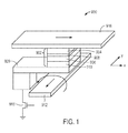
- FIG. 1 illustrates a perspective view of a magnetic cell 902 included in a memory device 900, according to an embodiment of the invention.
- the single magnetic cell 902 is illustrated in FIG. 1 , although it is contemplated that multiple magnetic cells 902 can be included in the memory device 900.
- the magnetic cell 902 may be a magnetic random access memory (MRAM) cell.
- MRAM magnetic random access memory
- the magnetic cell 902 can be implemented with one magnetization, namely a storage magnetization, that is aligned to represent the stored data value, and another magnetization, namely a sense magnetization, that is aligned to represent the target data value.
- the magnetic cell 902 can be implemented with the storage magnetization and a reference magnetization, which is typically a magnetization with a fixed direction.
- Conventional memories can be susceptible to unauthorized data access by using techniques to derive a charge state of a capacitor.
- the use of magnetization directions renders the memory device 900 less susceptible to such unauthorized data access, thereby further enhancing the level of security.
- Thermally assisted switching (TAS) technology provides one way of implementing the memory device 900 explained herein.
- a relatively small current is applied through the magnetic cell 902 to heat a pinning layer 910 by Ohmic effect.
- a temperature of the pinning layer 910 is above a threshold temperature, the storage magnetization direction is unpinned, thereby allowing a single bit to be programmed by applying a current through a field line 912 that is magnetically connected to the cell.
- a “0" can be stored by applying the current in one particular direction, and a "1” can be stored by applying the current in an opposite direction.
- the magnetic cell 902 is cooled below the threshold temperature, thereby pinning the storage magnetization in a programmed direction.
- the memory device 900 may be configured to support pattern checking.
- a "0" or a "1" is presented to the magnetic cell 902 by activating the field line 912 to switch the sense magnetization direction, in a manner consistent with directions used for the programming cycle.
- the cell has a typical resistance value of about 1 K ⁇ when the two magnetization directions are substantially parallel, and about 2 K ⁇ when the two magnetization directions are substantially antiparallel.
- the memory device 900 may program the storage magnetization relative to a reference magnetization, which typically has a fixed direction.
- a resistance of the magnetic tunnel junction is high, namely having a resistance value of typically about 2 K ⁇ corresponding to a high logic state "1".
- the resistance of the magnetic tunnel junction is low, namely having a resistance value of typically about 1 K ⁇ corresponding to a low logic state "0".
- a logic state of the magnetic cell 902 is read by comparing its resistance value to a reference resistance value, which is derived from a reference cell or a group of reference cells and represents an in-between resistance value between that of the high logic state "1" and the low logic state "0".
- the magnetic cell 902 is implemented as a magnetic tunnel junction, and includes a sense layer 904, a storage layer 906, and a layer 908 that is disposed between the sense layer 904 and the storage layer 906.
- Other implementations of the magnetic cell 902 are contemplated.
- the relative positioning of the sense layer 904 and the storage layer 906 can be reversed, with the storage layer 906 disposed above the sense layer 904.
- each of the sense layer 904 and the storage layer 906 includes, or is formed of, a magnetic material and, in particular, a magnetic material of the ferromagnetic type.
- a ferromagnetic material can be characterized by a substantially planar magnetization with a particular coercivity, which is indicative of a magnitude of a magnetic field to reverse the magnetization after it is driven to saturation in one direction.
- the sense layer 904 and the storage layer 906 can include the same ferromagnetic material or different ferromagnetic materials. As illustrated in FIG.
- the sense layer 904 can include a soft ferromagnetic material, namely one having a relatively low coercivity, while the storage layer 906 can include a hard ferromagnetic material, namely one having a relatively high coercivity.
- a magnetization of the sense layer 904 can be readily varied under low-intensity magnetic fields during pattern checking cycles, while a magnetization of the storage layer 906 remains stable.
- Suitable ferromagnetic materials include transition metals, rare earth elements, and their alloys, either with or without main group elements.
- suitable ferromagnetic materials include iron ("Fe"), cobalt ("Co"), nickel (“Ni”), and their alloys, such as permalloy (or Ni 80 Fe 20 ); alloys based on Ni, Fe, and boron (“B”); Co 90 Fe 10 ; and alloys based on Co, Fe, and B.
- alloys based on Ni and Fe (and optionally B) can have a smaller coercivity than alloys based on Co and Fe (and optionally B).
- a thickness of each of the sense layer 904 and the storage layer 906 can be in the nm range, such as from about 1 nm to about 20 nm or from about 1 nm to about 10 nm.
- sense layer 904 and the storage layer 906 are contemplated.
- sense layer 904 and the storage layer 906 can include multiple sub-layers in a fashion similar to that of the so-called synthetic antiferromagnetic layer.
- the magnetic cell 902 may include the storage layer 906 and a reference layer instead of the sense layer 904, with the layer 908 disposed between the storage layer 906 and the reference layer.
- Each of the reference layer and the storage layer 906 includes, or is formed of, a magnetic material and, in particular, a magnetic material of the ferromagnetic type, the characteristics of which are described previously with reference to FIG. 1 .
- the reference layer and the storage layer 906 can include the same ferromagnetic material or different ferromagnetic materials.
- the reference layer is different from the sense layer 904 in that the reference layer typically has a high coercivity, such as a coercivity higher than the storage layer 906.
- the layer 908 functions as a tunnel barrier, and includes, or is formed of, an insulating material. Suitable insulating materials include oxides, such as aluminum oxide (e.g., Al 2 O 3 ) and magnesium oxide (e.g., MgO). A thickness of the layer 908 can be in the nm range, such as from about 1 nm to about 10 nm.
- the magnetic cell 902 is implemented to store data corresponding to one of a pair of logic states.
- the magnetic cell 902 is a single-bit cell that stores a single-bit data value, although multi-bit implementations for storing multi-bit data values are also contemplated.
- the storage layer 906 has a storage magnetization that is switchable between a pair of directions corresponding to the pair of logic states.
- the magnetic cell 902 also includes the pinning layer 910, which is disposed adjacent to the storage layer 906 and, through exchange bias, stabilizes the storage magnetization along a particular one of the pair of directions when a temperature within, or in the vicinity of, the pinning layer 910 is lower than a temperature T BS .
- the temperature T BS can correspond to a blocking temperature, a Neel temperature, or another threshold temperature.
- the pinning layer 910 unpins, or decouples, the storage magnetization direction when the temperature is at, or above, the blocking temperature T BS , thereby allowing the storage magnetization direction to be switched to another one of the pair of directions.
- such a pinning layer is omitted adjacent to the sense layer 904, and, as a result, the sense layer 904 has a sense magnetization direction that is unpinned and is readily varied, with the substantial absence of exchange bias.
- the magnetic cell 902 includes a reference layer instead of the sense layer 904.
- an additional pinning layer may be disposed adjacent to the reference layer.
- This additional pinning layer may be characterized by a threshold temperature T BR , with T BR > T BS .
- the temperature T BR can correspond to a blocking temperature, a Neel temperature, or another threshold temperature.
- this additional pinning layer stabilizes the reference magnetization along a substantially fixed direction at temperatures lower than the threshold temperature T BR .
- the pinning layer 910 (and the additional pinning layer disposed adjacent to the reference layer in the alternative embodiment) includes, or is formed of, a magnetic material and, in particular, a magnetic material of the antiferromagnetic type.
- Suitable antiferromagnetic materials include transition metals and their alloys.
- suitable antiferromagnetic materials include alloys based on manganese ("Mn"), such as alloys based on iridium ("Ir") and Mn (e.g., IrMn); alloys based on Fe and Mn (e.g., FeMn); alloys based on platinum (“Pt”) and Mn (e.g., PtMn); and alloys based on Ni and Mn (e.g., NiMn).
- the blocking temperature T BS of alloys based on Ir and Mn can be in the range of about 120°C to about 220°C or about 150°C to about 200°C, and can be smaller than the blocking temperature T BS of alloys based on Pt and Mn (or based on Ni and Mn), which can be in the range of about 300°C to about 350°C.
- the memory device 900 also includes a set of traces (or strip conductors) to provide programming and pattern checking functions.
- a bit line 916 is electrically connected to the magnetic cell 902 on the side of the sense layer 904 (or, in an alternative embodiment, the reference layer) and is substantially orthogonal to the field line 912, which is disposed below and magnetically connected to the magnetic cell 902 on the side of the storage layer 906.
- the memory device 900 further includes a transistor 918, which is electrically connected, through a strap 920, to the magnetic cell 902 on the side of the storage layer 906.
- the transistor 918 is switchable between a blocked mode (OFF) and a conducting mode (ON), thereby allowing the flow of a current through the magnetic cell 902.
- OFF blocked mode
- ON conducting mode
- Other implementations of the memory device 900 are contemplated.
- the relative orientation of the bit line 916 and the field line 912 can be varied from that illustrated in FIG. 1 .
- the relative positioning of the bit line 916 and the field line 912 can be reversed, with the field line 912 disposed above the bit line 916.
- the magnetic cell 902 is heated by applying a heating current through the magnetic cell 902 via the bit line 916, with the transistor 918 in a conducting mode.
- the magnetic cell 902 is heated to a temperature above the blocking or threshold temperature T BS of the pinning layer 910, such that a magnetization of the storage layer 906 is unpinned.
- the magnetic cell 902 is heated to a temperature above the blocking or threshold temperature T BS of the pinning layer 910 but below the blocking or threshold temperature T BR of the additional pinning layer, such that a magnetization of the storage layer 906 is unpinned but the magnetization of the reference layer remains fixed.
- the field line 912 is activated to induce a write magnetic field to switch the storage magnetization from an initial direction to another direction. Specifically, a write current is applied through the field line 912 to induce the write magnetic field to switch the storage magnetization direction, according to a reference bit to be stored.
- the storage magnetization direction can be aligned according to the write magnetic field, the storage magnetization direction can be switched between multiple directions according to a programming encoding scheme.
- One possible encoding scheme is implemented with a pair of directions that are displaced by about 180°, such that a "0" is assigned to one of the pair of directions, and a "1" is assigned to another one of the pair of directions.
- the transistor 918 is switched to a blocked mode to inhibit current flow through the magnetic cell 902, thereby cooling the magnetic cell 902.
- the write magnetic field can be maintained during cooling of the magnetic cell 902, and can be deactivated once the magnetic cell 902 has cooled below the blocking temperature T BS of the pinning layer 910. Because the storage magnetization direction is pinned by the exchange bias of the pinning layer 910, its orientation remains stable so as to retain the stored data.
- the magnetic cell 902 can be implemented with an anisotropic shape having a relatively high aspect ratio, such as about 1.5 or more.
- the storage magnetization direction can be switched and can remain stable, without requiring the pinning layer 910.
- a programming cycle can be carried out by applying a write current through the magnetic cell 902 via the bit line 916, using the so-called spin transfer torque ("STT") effect.
- STT spin transfer torque
- the write current can become spin polarized by passing through a polarizing magnetic layer (not illustrated) or through the sense layer 904, and a magnetization of the storage layer 906 can be switched according to a spin-polarized orientation of the write current.
- Switching of the storage layer magnetization with the spin-polarized write current also can be combined with a TAS-type programming cycle, such as by heating the magnetic cell 902 above the blocking temperature T BS and then applying the spin-polarized write current through the magnetic cell 902.
- the memory device 900 may be configured to support pattern checking.
- the field line 912 is activated to induce a compare magnetic field to vary a magnetization of the sense layer 904. Specifically, a compare current is applied through the field line 912 to induce the compare magnetic field to vary the sense magnetization direction, according to a target bit to be compared with a reference bit. Because the sense layer 904 is subject to little or no exchange bias, the sense magnetization direction can be readily varied under low-intensity magnetic fields and at a temperature below the blocking temperature T BS , while the storage magnetization remains stable in a programmed direction.
- the field line 912 is activated to induce the compare magnetic field that is consistent with a programming encoding scheme. Because the sense magnetization direction can be aligned according to the compare magnetic field, the sense magnetization direction can be switched to a particular direction assigned to a "0" or a "1", according to the target bit presented for comparison.
- a degree of alignment between the sense magnetization direction and the storage magnetization direction is determined by applying a sense current through the magnetic cell 902 via the bit line 916, with the transistor 918 in a conducting mode. Measuring a resulting voltage across the magnetic cell 902 when the sense current is applied yields a resistance value of the magnetic cell 902 for a particular direction of the sense magnetization corresponding to a particular target bit. Alternatively, a resistance value can be determined by applying a voltage across the magnetic cell 902 and measuring a resulting current.
- a resistance value of the magnetic cell 902 typically corresponds to a maximum value, namely R max
- a resistance value of the magnetic cell 902 typically corresponds to a minimum value, namely R min .
- a resulting resistance value of the magnetic cell 902 can be compared with a reference resistance value R ref , which represents an in-between resistance value between R max and R min .
- a matching response of "yes” or “no” can be determined based on whether the resistance value of the magnetic cell 902 is greater than R ref , which indicates an antiparallel alignment between the magnetization directions, or smaller than R ref , which indicates a parallel alignment between the magnetization directions.
- the memory device 900 may program the storage magnetization relative to a reference magnetization, which typically has a fixed direction.
- a resistance of the magnetic tunnel junction is high, namely having a resistance value R max corresponding to a high logic state "1".
- R max a resistance value corresponding to a high logic state "1"
- R min a resistance value corresponding to a low logic state "0”.
- a logic state of a MRAM cell is read by comparing its resistance value to a reference resistance value R ref , which represents an in-between resistance value between that of the high logic state "1" and the low logic state "0".
- FIG. 2 illustrates a memory device 200 including multiple magnetic cells 902 that are magnetically coupled to the field line 912, according to an embodiment of the invention.
- a field line controller 930 may be coupled to the field line 912. As described further with reference to FIGS. 3 and 4 , the field line controller 930 may be configured to generate a write signal that traverses the field line 912. The write signal may be a write sequence, such as a sequence of current and/or voltage pulses. The write sequence may be for writing a multi-bit word to the multiple magnetic cells 902.
- a bit line controller 940 may be coupled to the bit lines 916. In one embodiment, the bit line controller 940 may generate a heating signal that traverses one or more of the bit lines 916. For example, the bit line controller 940 may switch on and off corresponding ones of the transistors 918, thereby turning on and off the flow of a current through corresponding ones of the magnetic cells 902.
- a single row of multiple magnetic cells 902A - 902N is illustrated in FIG. 2 , and the single row of multiple magnetic cells 902 is magnetically coupled to the single field line 912. It is contemplated that the memory device 200 may include additional rows of multiple magnetic cells 902 (see FIG. 5 ), where each of the additional rows is magnetically coupled to a corresponding additional field line 912. As previously described, the magnetic cell 902 may be a magnetic random access memory (MRAM) cell.
- MRAM magnetic random access memory
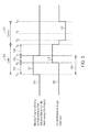
- FIG. 3 illustrates timing of a two-cycle write including a heating signal 370 (that may include one or more heating pulses) on one or more bit lines 916 corresponding to a first subset of bits included in a multi-bit word and having a first polarity, and a write sequence 360 (that may include one or more current pulses) on the field line 912 for writing the first subset of bits to a corresponding subset of the magnetic cells 902, according to an embodiment of the invention.
- a heating signal 370 that may include one or more heating pulses
- bit lines 916 corresponding to a first subset of bits included in a multi-bit word and having a first polarity
- a write sequence 360 that may include one or more current pulses
- the field line controller 930 is configured to generate the write sequence 360 for writing each bit in the multi-bit word to a corresponding one of the magnetic cells 902.
- the multi-bit word is written to the magnetic cells 902 in two write cycles, where each write cycle includes heating via bit lines 916 and writing via the field line 912.
- the heating via the bit lines 916 may be controlled by the bit line controller 940.
- the writing via the field line 912 may be controlled by the field line controller 930.
- a first write cycle 320 at least a subset of the magnetic cells 902 corresponding to the first subset of bits in the multi-bit word are written to the first polarity.
- the magnetic cells 902 corresponding to the second subset of bits in the multi-bit word may also be written to the first polarity.
- a second write cycle 322 subsequent to the first write cycle 320 a remaining subset of the magnetic cells 902 corresponding to the second subset of bits in the multi-bit word are written to the second polarity.
- the subset of the magnetic cells 902 corresponding to the first subset of bits in the multi-bit word are not heated by the bit lines 916, and are not written to by the field line 912.
- the write sequence 360 traversing the single field line 912 can thereby write a multi-bit word to the magnetic cells 902 in two write cycles.
- the heating signal 370 may include a heating pulse 311 that may be applied to a subset of the magnetic cells 902 corresponding to the first subset of bits in the multi-bit word via corresponding bit lines 916.
- the heating pulse 311 may heat the subset of the magnetic cells for a heating time period 340 during the first write cycle 320.
- the heating signal 372 may include a heating pulse 331 that may be applied to a remaining subset of the magnetic cells 902 corresponding to the second subset of bits in the multi-bit word via corresponding bit lines 916.
- the heating pulse 331 may heat the remaining subset of the magnetic cells 902 for a pre-heating time period 350 during the first write cycle 320, and may heat the remaining subset of the magnetic cells 902 for a heating time period 342 during the second write cycle 322.
- the bit line controller 940 may be configured to switch the transistors 918 between a blocked mode (OFF) and a conducting mode (ON), thereby allowing the flow of the heating pulses 311 and/or 331 through the magnetic cells 902 (via the bit lines 916) in the conducting mode.
- the heating pulses 311 and 331 heat the pinning layer 910 (see FIG.
- Each heating pulse 311 may be applied for the time period 340.
- the time period 340 may extend from time T A to time T C .
- Each heating pulse 331 may be applied for the pre-heating time period 350 and the heating time period 342.
- the pre-heating time period 350 may extend from time T A to time T D
- the heating time period 342 may extend from time T D to time T F .
- a duration of the pre-heating time period 350 is longer than a duration of the time period 340.
- the heating time period 342 during the second write cycle 322 is continuous with (overlaps with) the pre-heating time period 350 during the first write cycle 320.
- the write sequence 360 may include a current pulse 312 that may be applied on the field line 912 from time T B to time T D , where time T B is between time T A and time T C , and time T D is after time T C .
- the current pulse 312 may be applied on the field line 912 from time T A to time T D .
- a time duration 300 from time T A to time T B may be in the range from about 10 nanoseconds to about 20 nanoseconds, such as about 10 nanoseconds, about 11 nanoseconds, about 12 nanoseconds, about 13 nanoseconds, about 14 nanoseconds, about 15 nanoseconds, about 16 nanoseconds, about 17 nanoseconds, about 18 nanoseconds, about 19 nanoseconds, or about 20 nanoseconds.
- a time duration 302 from time T B to time T C may be in the range from about 4 nanoseconds to about 8 nanoseconds, such as about 4 nanoseconds, about 5 nanoseconds, about 6 nanoseconds, about 7 nanoseconds, or about 8 nanoseconds.
- a time duration 304 from time T C to time T D may be in the range from about 4 nanoseconds to about 8 nanoseconds, such as about 4 nanoseconds, about 5 nanoseconds, about 6 nanoseconds, about 7 nanoseconds, or about 8 nanoseconds.
- the time duration of the heating time period 340 during the first write cycle 320 (which may be from time T A to time T C ) may be in the range from about 14 nanoseconds to about 28 nanoseconds, such as about 14 nanoseconds, about 15 nanoseconds, about 20 nanoseconds, about 25 nanoseconds, or about 28 nanoseconds.
- the current pulse 312 included in the write sequence 360 may write concurrently to the at least a subset of the magnetic cells 902 corresponding to the first subset of bits in the multi-bit word.
- the current pulse 312 may write these magnetic cells 902 to the first polarity.
- the current pulse 312 may write the magnetic cells 902A - 902N (corresponding to all bits in the multi-bit word) to the first polarity.
- the subset of the magnetic cells 902 corresponding to the first subset of bits in the multi-bit word are not heated from time T C until the end of the first write cycle 320, and are also not heated during the second write cycle 322.
- the subset of the magnetic cells 902 corresponding to the first subset of bits in the multi-bit word thereby cools below the threshold temperature before a start of the current pulse 314 (time T E ), pinning the storage magnetization of these magnetic cells 902 in a direction corresponding to the first polarity.
- the current pulse 314 (included in the write sequence 360) on the field line 912 therefore does not affect the storage magnetization stored in these magnetic cells 912.
- the remaining subset of the magnetic cells corresponding to the second subset of bits in the multi-bit word are continuously heated from time T A at the start of the first write cycle 320 until time T F during the second write cycle 322.
- a time extent of the heating pulse 331 during the second write cycle 322 can be reduced from a time extent of the heating pulse during the first write cycle 320 (time T A to time T D ).
- a time duration 306 may be shorter than the time duration 300, while a time duration 308 may be equal to or approximately equal to the time duration 302.
- a time duration of the second write cycle 322 can therefore be shorter than a time duration of the first write cycle 320, thus increasing a speed of the two-cycle write.
- a current pulse 314 may be applied on the field line 912 from time T E to time T G , where time T E is between time T D and time T F , and time T G is after time T F .
- the current pulse 312 may be applied on the field line 912 from time T D to time T G .
- the time duration 306 from time T D to time T E may be in the range from about 1 nanosecond to about 5 nanoseconds, such as about 1 nanosecond, about 2 nanoseconds, about 3 nanoseconds, about 4 nanoseconds, or about 5 nanoseconds.
- the time duration 306 may be zero (time T D equal to time T E ) or approximately zero.
- the time duration 308 from time T E to time T F may be in the range from about 4 nanoseconds to about 8 nanoseconds, such as about 4 nanoseconds, about 5 nanoseconds, about 6 nanoseconds, about 7 nanoseconds, or about 8 nanoseconds.
- the time duration 310 from time T F to time T G may be in the range from about 4 nanoseconds to about 8 nanoseconds, such as about 4 nanoseconds, about 5 nanoseconds, about 6 nanoseconds, about 7 nanoseconds, or about 8 nanoseconds.
- the time duration of the heating time period 342 during the second write cycle 322 (which may be from time T D to time T F ) may be in the range from about 5 nanoseconds to about 13 nanoseconds, such as about 5 nanoseconds, about 8 nanoseconds, about 10 nanoseconds, and about 13 nanoseconds. Because the remaining subset of the magnetic cells 902 (see FIG. 2 ) has been pre-heated during the pre-heating time period 350 during the first write cycle 320, the time duration of the heating time period 342 during the second write cycle 322 may be less than the time duration of the heating time period 340 during the first write cycle 320 (for the subset of the magnetic cells 902 that have not been pre-heated). As described previously, for this reason a time duration of the second write cycle 322 can therefore be shorter than a time duration of the first write cycle 320, thus increasing a speed of the two-cycle write.
- the current pulse 314 on the field line 912 may write concurrently to the remaining subset of the magnetic cells 902 corresponding to the second subset of bits in the multi-bit word.
- the current pulse 314 writes these magnetic cells 902 to the second polarity.
- the subset of the magnetic cells 902 corresponding to the first subset of bits in the multi-bit word are not heated by the bit lines 916, and are not written to by the field line 912.
- the two-cycle write of a multi-bit word to the magnetic cells 902 with a single field line 912 reduces power consumption relative to writing the multi-bit word to the magnetic cells 902 with multiple field lines (such as a separate field line per magnetic cell 902).
- the field line 912 may use a bidirectional current pulse with an average current amplitude of zero or approximately zero, the electromagnetic performance of the field 912 can be enhanced.
- the two-cycle write can be suitable for high-speed applications.
- the first write cycle 320 can begin before the multi-bit word to be written is known (and/or received by the memory device 200), such as during a turnaround time of a data bus on which the multi-bit word is to be provided.
- the time duration of the second write cycle 322 can be reduced because the magnetic cells 902 may already be heated during the first write cycle 320.
- the heating pulse 331 may not extend from time T A to time T F , but instead may be divided into two current pulses separated by a cooling period.
- the cooling period may extend from time T C to time T D , or may extend for a portion of the time between time T C and time T D .
- This cooling period may result in an increased time duration of the second write cycle 322 (because the magnetic cells 902 will have at least partially cooled down at the start of the second write cycle 322).
- this cooling period may save power. Power savings can be realized if a time duration of the first write cycle 320 is sufficiently long, such that the increase in the time duration of the second write cycle 322 is less than a duration of the cooling period.
- the heating pulse 331 may extend from time T D to time T F , such that the remaining subset of the magnetic cells 902 are not written to the first polarity during the first write cycle 320. Because the remaining subset of the magnetic cells 902 are not heated during the first write cycle 320 in this embodiment, power can be saved. At the same time, because the remaining subset of the magnetic cells 902 have not been heated during the first write cycle 320, the time duration of the second write cycle 322 may increase.
- the memory device 200 may include additional rows of multiple magnetic cells 902, where each of the additional rows is magnetically coupled to a corresponding additional field line 912. Multiple multi-bit words can be concurrently written to multiple rows of the magnetic cells 902 based on a multi-cycle write based on principles of the two-cycle write described with reference to FIGS. 3 and 4 .
- FIG. 5 illustrates an example.
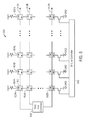
- a memory device 500 including an array of magnetic cells 902 and a plurality of field lines 912 is illustrated, according to an embodiment of the invention.
- the array of magnetic cells 902 includes a plurality of rows 502 and a plurality of columns 504.
- a field line controller 530 may be coupled to the plurality of field lines 912, and may generate a write signal that traverses each of the field lines 912.
- a bit line controller 540 may be coupled to the plurality of bit lines 916, and may generate a heating signal that traverses each of the bit lines 916. Based on principles of the two-cycle write described with reference to FIGS. 3 and 4 , the write signals generated by the field line controller 530 and the heating signals generated by the bit line controller 540 may write multiple multi-bit words to the multiple rows 502 of magnetic cells 902.
- the field line controller 530 generates write signals that write N multi-bit words to N corresponding rows of the magnetic cells 902 in 2 N write cycles.
- N 2
- the magnetic cells 902 can be disposed in an array having two rows and M columns (where M is the number of bits in each multi-bit word), with each of two field lines 912 being magnetically coupled to a corresponding row of the magnetic cells 902, and each of M bit lines 916 being electrically connected to a corresponding column of the magnetic cells 902.
- the magnetic cells 902 are heated by the M bit lines 916, and the two field lines can write the two rows of the magnetic cells 902 to a first combination of values (0, 0), respectively, where 0 refers to the first polarity.
- the magnetic cells 902 are heated, except for any column of the magnetic cells 902 that corresponds to values of (0, 0) in the two multi-bit words, as those columns of the magnetic cells 902 need not be perturbed further.
- the two field lines can write each of the remaining rows of the magnetic cells 902 to a second combination of values, such as (0, 1), respectively, where 1 refers to the second polarity.
- the magnetic cells 902 are heated, except for any column of the magnetic cells 902 that corresponds to values of (0, 0) or (0, 1) in the two multi-bit words, as those columns of the magnetic cells 902 need not be perturbed further.
- the two field lines can write each of the remaining rows of the magnetic cells 902 to a third combination of two values, such as (1, 0), respectively.
- the magnetic cells 902 are heated, except for any column of the magnetic cells 902 that corresponds to values of (0, 0), (0, 1), or (1, 0) in the two multi-bit words, as those columns of the magnetic cells 902 need not be perturbed further.
- the two field lines can write each of the remaining rows of the magnetic cells 902 to a fourth combination of two values, such as (1, 1), respectively. Therefore, it can be seen that two field lines 912 can write two multi-bit words to two corresponding rows of the magnetic cells 902 in 4 (2 2 ) write cycles. Similarly, this example can be extended to N field lines 912, where N is greater than 2. As described previously, the N field lines 912 can write N multi-bit words to N corresponding rows of the magnetic cells 902 in 2 N write cycles.
- each of a plurality of write signals writes concurrently to corresponding ones of the plurality of rows 502 of the magnetic cells 902 such that each of at least a first subset of the plurality of columns 504 of the magnetic cells 902 is configured to a first state.
- the first state is (0, 0)
- the first state is (0, 1)
- the first state is (1, 0).
- the first state may be any combination of N values (one value per row 502).
- each of the plurality of columns 504 of the magnetic cells 902 may be configured to the first state.
- a first subset of the plurality of columns 504 of the magnetic cells 902 may be configured to the first state.
- each of the plurality of write signals writes concurrently to the each of the plurality of rows 502 of the magnetic cells 902 such that each of a second subset of the plurality of columns 504 of the magnetic cells 902 is configured to an updated state.
- the first state is (0, 0)
- the updated state may be any of (0, 1), (1, 0), or (1, 1).
- Each of the first subset of the plurality of columns 504 may remain configured to the first state.
- each of the first subset of the plurality of columns 504 may already store corresponding bit values ((0, 0) in this example) located at a bit position in each of the two multi-bit words that is associated with the first subset of the plurality of columns 504.
- the first subset of the plurality of columns 504 therefore need not be perturbed further, and can be excluded from the subsequent write cycle.
- the bit line controller 540 may generate a plurality of heating signals that traverse corresponding ones of the second subset of the plurality of bit lines 916 electrically connected to corresponding ones of the second subset of the plurality of columns 504 of the magnetic cells 902.
Landscapes
- Engineering & Computer Science (AREA)
- Computer Hardware Design (AREA)
- Microelectronics & Electronic Packaging (AREA)
- Mram Or Spin Memory Techniques (AREA)
- Hall/Mr Elements (AREA)
Claims (10)
- Speichervorrichtung (200, 500), umfassend:eine Vielzahl magnetischer Direktzugriffsspeicher- ("MRAM"-) Zellen (902);eine Vielzahl von Bitleitungen (916), wobei jede der Vielzahl von Bit-Leitungen mit einer entsprechenden einen aus der Vielzahl von MRAM-Zellen elektrisch verbunden ist;eine Bitleitungssteuerung (940, 540);eine Feldleitung (912) sowieeine Feldleitungssteuerung (930, 530), die konfiguriert ist, um eine Schreibsequenz (360) zu erzeugen, welche die Feldleitung durchläuft, wobei die Schreibsequenz dazu geeignet ist, ein erstes Wort aus mehreren Bits auf die Vielzahl von MRAM-Zellen zu schreiben, wobei das Wort aus mehreren Bits eine erste Untergruppe von Bits mit einer ersten Polarität und eine zweite Untergruppe von Bits mit einer zweiten Polarität umfasst;worin die Schreibsequenz gleichzeitig auf zumindest eine Untergruppe der Vielzahl von MRAM-Zellen schreibt, die der ersten Untergruppe von Bits mit der ersten Polarität entspricht, um die Untergruppe der Vielzahl von MRAM-Zellen in der ersten Polarität auszurichten, danach anschließend gleichzeitig auf eine restliche Untergruppe der Vielzahl von MRAM-Zellen schreibt, welche der zweiten Untergruppe von Bits mit der zweiten Polarität entspricht, um die verbleibende Untergruppe der Vielzahl von MRAM-Zellen in der zweiten Polarität auszurichten; undworin die Bitleitungssteuerung konfiguriert ist, um ein erstes Heizsignal (370) zu erzeugen, welches jede aus zumindest einer Untergruppe der Vielzahl von Bitleitungen durchläuft, die mit entsprechenden aus der zumindest einen Untergruppe der Vielzahl von MRAM-Zellen elektrisch verbunden sind, worin das erste Heizsignal jede aus der zumindest einen Untergruppe der Vielzahl von MRAM-Zellen über eine Heizzeitspanne während eines ersten Schreibzyklus aufheizt;worin die Bitleitungssteuerung konfiguriert ist, um ein zweites Heizsignal (372) zu erzeugen, welches jede aus einer restlichen Untergruppe der Vielzahl von Bitleitungen durchläuft, die mit entsprechenden aus der restlichen Untergruppe der Vielzahl von MRAM-Zellen elektrisch verbunden sind, worin das zweite Heizsignal jede aus der restlichen Untergruppe der Vielzahl von MRAM-Zellen über eine Vorheizzeitspanne während des ersten Schreibzyklus vorheizt und jede aus der restlichen Untergruppe der Vielzahl von MRAM-Zellen über eine Heizzeitspanne während des zweiten Schreibzyklus, die kürzer als die Heizzeitspanne während des ersten Schreibzyklus ist, aufheizt, sodass eine Dauer des zweiten Schreibzyklus kürzer als eine Dauer des ersten Schreibzyklus ist.
- Speichervorrichtung nach Anspruch 1, worin die Heizzeitspanne während des zweiten Schreibzyklus ohne Unterbrechung auf die Vorheizzeitspanne während des ersten Schreibzyklus folgt.
- Speichervorrichtung nach Anspruch 1, worin die Heizzeitspanne während des zweiten Schreibzyklus von der Vorheizzeitspanne während des ersten Schreibzyklus durch eine Abkühlzeit für die restliche Untergruppe der Vielzahl von MRAM-Zellen getrennt ist.
- Speichervorrichtung nach Anspruch 1, worin eine Dauer der Vorheizzeitspanne während des ersten Schreibzyklus länger als eine Dauer der Heizzeitspanne während des ersten Schreibzyklus ist.
- Speichervorrichtung nach Anspruch 1, worin:die Schreibsequenz einen Stromimpuls umfasst, welcher die Feldleitung durchläuft, wobei der Stromimpuls dazu geeignet ist, um auf die zumindest eine Untergruppe der Vielzahl von MRAM-Zellen zu schreiben; undsich die Vorheizzeitspanne während des ersten Schreibzyklus von einem ersten Zeitpunkt vor einem Startzeitpunkt des Stromimpulses bis zu einem zweiten Zeitpunkt während des Stromimpulses erstreckt.
- Speichervorrichtung nach Anspruch 1, worin:die Vielzahl von MRAM-Zellen in einer Matrix aus MRAM-Zellen angeordnet sind, wobei die Matrix eine Vielzahl von Zeilen und eine Vielzahl von Spalten umfasst; unddie Speichervorrichtung eine Vielzahl von Feldleitungen (912) umfasst;die Feldleitungssteuerung konfiguriert ist, um eine Vielzahl von Schreibsignalen zu erzeugen, wobei jedes der Vielzahl von Schreibsignalen eine entsprechende eine aus der Vielzahl von Feldleitungen durchläuft;worin:in einem anfänglichen Schreibzyklus jedes der Vielzahl von Schreibsignalen gleichzeitig auf eine entsprechende eine aus der Vielzahl von Zeilen aus MRAM-Zellen schreibt, sodass jede aus zumindest einer ersten Untergruppe der Vielzahl von Spalten aus MRAM-Zellen in einer ersten Polarität ausgerichtet wird; undin einem anschließenden Schreibzyklus jedes aus der Vielzahl von Schreibsignalen gleichzeitig auf die entsprechende eine aus der Vielzahl von Zeilen aus MRAM-Zellen schreibt, sodass jede aus einer zweiten Untergruppe der Vielzahl von Spalten aus MRAM-Zellen in einer zweiten Polarität ausgerichtet wird, während jede aus der ersten Untergruppe der Vielzahl von Spalten aus MRAM-Zellen in der ersten Polarität ausgerichtet wird.
- Speichervorrichtung nach Anspruch 6, worin in dem anfänglichen Schreibzyklus jedes der Vielzahl von Schreibsignalen gleichzeitig auf die entsprechende eine aus der Vielzahl von Zeilen aus MRAM-Zellen schreibt, sodass jede aus der Vielzahl von Spalten aus MRAM-Zellen in der ersten Polarität ausgerichtet wird.
- Speichervorrichtung nach Anspruch 6, worin jedes aus der Vielzahl von Schreibsignalen ein entsprechendes eines aus einer ersten Vielzahl von Wörtern mit mehreren Bits auf die entsprechende eine aus der Vielzahl von Zeilen aus MRAM-Zellen schreibt, sodass jede aus der Vielzahl von Spalten aus MRAM-Zellen entsprechende Bitwerte speichert, die sich an einer Bitposition in jedem aus der ersten Vielzahl von Wörtern mit mehreren Bits befinden, die einer entsprechenden einen aus der Vielzahl von Spalten aus MRAM-Zellen zugeordnet ist.
- Speichervorrichtung nach Anspruch 8, worin jede aus der ersten Untergruppe der Vielzahl von Spalten aus MRAM-Zellen aus dem anschließenden Schreibzyklus ausgeschlossen wird, weil im anfänglichen Schreibzyklus jede aus der ersten Untergruppe der Vielzahl von Spalten aus MRAM-Zellen bereits auf die entsprechenden Bitwerte konfiguriert wurde, die sich an der Bitposition in jedem aus der ersten Vielzahl von Wörtern aus mehreren Bits befinden, die der entsprechenden einen aus der ersten Untergruppe der Vielzahl von Spalten aus MRAM-Zellen zugeordnet ist.
- Speichervorrichtung nach Anspruch 6, welche ferner umfasst:eine Vielzahl von Bitleitungen, wobei jede aus der Vielzahl von Bitleitungen mit einer entsprechenden einen aus der Vielzahl von MRAM-Zellen elektrisch verbunden ist; undeine Bitleitungssteuerung, worin die Bitleitungssteuerung im anschließenden Schreibzyklus konfiguriert ist, um eine Vielzahl von Heizsignalen zu erzeugen, die entsprechende aus einer Untergruppe der Vielzahl von Bitleitungen durchlaufen, welche mit entsprechenden aus der zweiten Untergruppe der Vielzahl von Spalten aus MRAM-Zellen elektrisch verbunden sind.
Applications Claiming Priority (2)
| Application Number | Priority Date | Filing Date | Title |
|---|---|---|---|
| US201161545469P | 2011-10-10 | 2011-10-10 | |
| PCT/US2012/059370 WO2013055695A1 (en) | 2011-10-10 | 2012-10-09 | Apparatus, system, and method for writing multiple magnetic random access memory cells with a single field line |
Publications (3)
| Publication Number | Publication Date |
|---|---|
| EP2766906A1 EP2766906A1 (de) | 2014-08-20 |
| EP2766906A4 EP2766906A4 (de) | 2015-03-11 |
| EP2766906B1 true EP2766906B1 (de) | 2016-03-30 |
Family
ID=48082345
Family Applications (1)
| Application Number | Title | Priority Date | Filing Date |
|---|---|---|---|
| EP12839765.0A Active EP2766906B1 (de) | 2011-10-10 | 2012-10-09 | Vorrichtung, system und verfahren zum schreiben auf mehrere magnetische direktzugriffsspeicherzellen mit einer einzigen feldlinie |
Country Status (5)
| Country | Link |
|---|---|
| US (1) | US8902643B2 (de) |
| EP (1) | EP2766906B1 (de) |
| BR (1) | BR112014008719A2 (de) |
| TW (1) | TW201331937A (de) |
| WO (1) | WO2013055695A1 (de) |
Families Citing this family (10)
| Publication number | Priority date | Publication date | Assignee | Title |
|---|---|---|---|---|
| US9287003B2 (en) * | 2013-12-06 | 2016-03-15 | Rambus Inc. | Multi-cycle write leveling |
| EP2905783B1 (de) | 2014-02-06 | 2018-09-19 | Crocus Technology S.A. | Verfahren zum Schreiben mit Verbesserung der Reproduzierbarkeit eines Multibit TAS MRAM mit selbstbezogener Leseoperation |
| US9520192B2 (en) * | 2014-06-30 | 2016-12-13 | Intel Corporation | Resistive memory write operation with merged reset |
| EP3040999A1 (de) | 2014-07-17 | 2016-07-06 | Crocus Technology Inc. | Vorrichtung und verfahren zum entwerfen magnetfeldsensorelementen-layout in sensoren |
| EP3040735A1 (de) | 2014-07-17 | 2016-07-06 | Crocus Technology Inc. | Vorrichtung, system und verfahren zur erfassung von kommunikationssignalen mit magnetfeldmesselementen |
| EP3040997A1 (de) * | 2014-07-17 | 2016-07-06 | Crocus Technology Inc. | Vorrichtung und verfahren zur messung eines magnetfelds mithilfe von anordnungen von magnetfeldmesselementen |
| US9720057B2 (en) | 2014-07-17 | 2017-08-01 | Crocus Technology Inc. | Apparatus and method for sensing a magnetic field using subarrays of magnetic field sensing elements for high voltage applications |
| US9689936B2 (en) | 2014-07-17 | 2017-06-27 | Crocus Technology Inc. | Apparatus and method for sensing a magnetic field using subarrays of magnetic sensing elements |
| US9524765B2 (en) | 2014-08-15 | 2016-12-20 | Qualcomm Incorporated | Differential magnetic tunnel junction pair including a sense layer with a high coercivity portion |
| US10818330B2 (en) | 2019-01-31 | 2020-10-27 | Avalanche Technology, Inc. | Fast programming of magnetic random access memory (MRAM) |
Family Cites Families (12)
| Publication number | Priority date | Publication date | Assignee | Title |
|---|---|---|---|---|
| US6256224B1 (en) | 2000-05-03 | 2001-07-03 | Hewlett-Packard Co | Write circuit for large MRAM arrays |
| US6603678B2 (en) * | 2001-01-11 | 2003-08-05 | Hewlett-Packard Development Company, L.P. | Thermally-assisted switching of magnetic memory elements |
| CN1860520B (zh) * | 2003-05-20 | 2011-07-06 | 辛迪安特公司 | 数字底板 |
| US7180770B2 (en) | 2005-03-24 | 2007-02-20 | Hewlett-Packard Development Company, L.P. | Series diode thermally assisted MRAM |
| US7362644B2 (en) * | 2005-12-20 | 2008-04-22 | Magic Technologies, Inc. | Configurable MRAM and method of configuration |
| US7532505B1 (en) * | 2006-07-17 | 2009-05-12 | Grandis, Inc. | Method and system for using a pulsed field to assist spin transfer induced switching of magnetic memory elements |
| US7502249B1 (en) * | 2006-07-17 | 2009-03-10 | Grandis, Inc. | Method and system for using a pulsed field to assist spin transfer induced switching of magnetic memory elements |
| TWI449040B (zh) | 2006-10-06 | 2014-08-11 | Crocus Technology Sa | 用於提供內容可定址的磁阻式隨機存取記憶體單元之系統及方法 |
| US20090213643A1 (en) | 2008-02-26 | 2009-08-27 | Michael Angerbauer | Integrated Circuit and Method of Improved Determining a Memory State of a Memory Cell |
| US8031519B2 (en) * | 2008-06-18 | 2011-10-04 | Crocus Technology S.A. | Shared line magnetic random access memory cells |
| US8228703B2 (en) * | 2008-11-04 | 2012-07-24 | Crocus Technology Sa | Ternary Content Addressable Magnetoresistive random access memory cell |
| US8488377B2 (en) * | 2009-11-11 | 2013-07-16 | Ocz Technology Group Inc. | Mass storage device with solid-state memory components capable of increased endurance |
-
2012
- 2012-10-09 EP EP12839765.0A patent/EP2766906B1/de active Active
- 2012-10-09 WO PCT/US2012/059370 patent/WO2013055695A1/en not_active Ceased
- 2012-10-09 TW TW101137356A patent/TW201331937A/zh unknown
- 2012-10-09 US US13/648,221 patent/US8902643B2/en active Active
- 2012-10-09 BR BR112014008719A patent/BR112014008719A2/pt not_active IP Right Cessation
Also Published As
| Publication number | Publication date |
|---|---|
| US20130094283A1 (en) | 2013-04-18 |
| BR112014008719A2 (pt) | 2017-04-18 |
| TW201331937A (zh) | 2013-08-01 |
| EP2766906A1 (de) | 2014-08-20 |
| EP2766906A4 (de) | 2015-03-11 |
| US8902643B2 (en) | 2014-12-02 |
| WO2013055695A1 (en) | 2013-04-18 |
Similar Documents
| Publication | Publication Date | Title |
|---|---|---|
| US8902643B2 (en) | Apparatus, system, and method for writing multiple magnetic random access memory cells with a single field line | |
| US8625336B2 (en) | Memory devices with series-interconnected magnetic random access memory cells | |
| US8488372B2 (en) | Magnetic random access memory devices including multi-bit cells | |
| US8576615B2 (en) | Magnetic random access memory devices including multi-bit cells | |
| US8611140B2 (en) | Magnetic random access memory devices including shared heating straps | |
| US9818465B2 (en) | Self-referenced memory device and method using spin-orbit torque for reduced size | |
| EP2942780B1 (de) | Multibit-MRAM-Zelle und Verfahren zum Schreiben und Lesen einer solchen MRAM-Zelle | |
| EP2528060B1 (de) | Mehrbit-Zelle mit synthetischer Speicherschicht | |
| EP2673779B1 (de) | Für selbstbezogene leseoperationen konfigurierte magnetische direktzugriffspeicheranordnungen | |
| EP2758960B1 (de) | Direktzugriffs-magnetspeichervorrichtungen mit erwärmungsstreifen | |
| US9054029B2 (en) | Memory devices with magnetic random access memory (MRAM) cells and associated structures for connecting the MRAM cells | |
| EP2905783B1 (de) | Verfahren zum Schreiben mit Verbesserung der Reproduzierbarkeit eines Multibit TAS MRAM mit selbstbezogener Leseoperation |
Legal Events
| Date | Code | Title | Description |
|---|---|---|---|
| PUAI | Public reference made under article 153(3) epc to a published international application that has entered the european phase |
Free format text: ORIGINAL CODE: 0009012 |
|
| 17P | Request for examination filed |
Effective date: 20140328 |
|
| AK | Designated contracting states |
Kind code of ref document: A1 Designated state(s): AL AT BE BG CH CY CZ DE DK EE ES FI FR GB GR HR HU IE IS IT LI LT LU LV MC MK MT NL NO PL PT RO RS SE SI SK SM TR |
|
| DAX | Request for extension of the european patent (deleted) | ||
| A4 | Supplementary search report drawn up and despatched |
Effective date: 20150206 |
|
| RIC1 | Information provided on ipc code assigned before grant |
Ipc: G11C 11/16 20060101AFI20150202BHEP |
|
| REG | Reference to a national code |
Ref country code: DE Ref legal event code: R079 Ref document number: 602012016437 Country of ref document: DE Free format text: PREVIOUS MAIN CLASS: G11C0011060000 Ipc: G11C0011160000 |
|
| GRAP | Despatch of communication of intention to grant a patent |
Free format text: ORIGINAL CODE: EPIDOSNIGR1 |
|
| RIC1 | Information provided on ipc code assigned before grant |
Ipc: G11C 11/16 20060101AFI20150828BHEP |
|
| INTG | Intention to grant announced |
Effective date: 20150916 |
|
| GRAS | Grant fee paid |
Free format text: ORIGINAL CODE: EPIDOSNIGR3 |
|
| GRAA | (expected) grant |
Free format text: ORIGINAL CODE: 0009210 |
|
| AK | Designated contracting states |
Kind code of ref document: B1 Designated state(s): AL AT BE BG CH CY CZ DE DK EE ES FI FR GB GR HR HU IE IS IT LI LT LU LV MC MK MT NL NO PL PT RO RS SE SI SK SM TR |
|
| REG | Reference to a national code |
Ref country code: GB Ref legal event code: FG4D |
|
| REG | Reference to a national code |
Ref country code: CH Ref legal event code: EP |
|
| REG | Reference to a national code |
Ref country code: AT Ref legal event code: REF Ref document number: 786128 Country of ref document: AT Kind code of ref document: T Effective date: 20160415 |
|
| REG | Reference to a national code |
Ref country code: IE Ref legal event code: FG4D |
|
| REG | Reference to a national code |
Ref country code: DE Ref legal event code: R096 Ref document number: 602012016437 Country of ref document: DE |
|
| REG | Reference to a national code |
Ref country code: LT Ref legal event code: MG4D |
|
| PG25 | Lapsed in a contracting state [announced via postgrant information from national office to epo] |
Ref country code: NO Free format text: LAPSE BECAUSE OF FAILURE TO SUBMIT A TRANSLATION OF THE DESCRIPTION OR TO PAY THE FEE WITHIN THE PRESCRIBED TIME-LIMIT Effective date: 20160630 Ref country code: GR Free format text: LAPSE BECAUSE OF FAILURE TO SUBMIT A TRANSLATION OF THE DESCRIPTION OR TO PAY THE FEE WITHIN THE PRESCRIBED TIME-LIMIT Effective date: 20160701 Ref country code: HR Free format text: LAPSE BECAUSE OF FAILURE TO SUBMIT A TRANSLATION OF THE DESCRIPTION OR TO PAY THE FEE WITHIN THE PRESCRIBED TIME-LIMIT Effective date: 20160330 Ref country code: FI Free format text: LAPSE BECAUSE OF FAILURE TO SUBMIT A TRANSLATION OF THE DESCRIPTION OR TO PAY THE FEE WITHIN THE PRESCRIBED TIME-LIMIT Effective date: 20160330 |
|
| REG | Reference to a national code |
Ref country code: NL Ref legal event code: MP Effective date: 20160330 |
|
| REG | Reference to a national code |
Ref country code: AT Ref legal event code: MK05 Ref document number: 786128 Country of ref document: AT Kind code of ref document: T Effective date: 20160330 |
|
| PG25 | Lapsed in a contracting state [announced via postgrant information from national office to epo] |
Ref country code: SE Free format text: LAPSE BECAUSE OF FAILURE TO SUBMIT A TRANSLATION OF THE DESCRIPTION OR TO PAY THE FEE WITHIN THE PRESCRIBED TIME-LIMIT Effective date: 20160330 Ref country code: RS Free format text: LAPSE BECAUSE OF FAILURE TO SUBMIT A TRANSLATION OF THE DESCRIPTION OR TO PAY THE FEE WITHIN THE PRESCRIBED TIME-LIMIT Effective date: 20160330 Ref country code: LV Free format text: LAPSE BECAUSE OF FAILURE TO SUBMIT A TRANSLATION OF THE DESCRIPTION OR TO PAY THE FEE WITHIN THE PRESCRIBED TIME-LIMIT Effective date: 20160330 Ref country code: LT Free format text: LAPSE BECAUSE OF FAILURE TO SUBMIT A TRANSLATION OF THE DESCRIPTION OR TO PAY THE FEE WITHIN THE PRESCRIBED TIME-LIMIT Effective date: 20160330 |
|
| REG | Reference to a national code |
Ref country code: FR Ref legal event code: PLFP Year of fee payment: 5 |
|
| PG25 | Lapsed in a contracting state [announced via postgrant information from national office to epo] |
Ref country code: NL Free format text: LAPSE BECAUSE OF FAILURE TO SUBMIT A TRANSLATION OF THE DESCRIPTION OR TO PAY THE FEE WITHIN THE PRESCRIBED TIME-LIMIT Effective date: 20160330 |
|
| PG25 | Lapsed in a contracting state [announced via postgrant information from national office to epo] |
Ref country code: EE Free format text: LAPSE BECAUSE OF FAILURE TO SUBMIT A TRANSLATION OF THE DESCRIPTION OR TO PAY THE FEE WITHIN THE PRESCRIBED TIME-LIMIT Effective date: 20160330 Ref country code: IS Free format text: LAPSE BECAUSE OF FAILURE TO SUBMIT A TRANSLATION OF THE DESCRIPTION OR TO PAY THE FEE WITHIN THE PRESCRIBED TIME-LIMIT Effective date: 20160730 Ref country code: PL Free format text: LAPSE BECAUSE OF FAILURE TO SUBMIT A TRANSLATION OF THE DESCRIPTION OR TO PAY THE FEE WITHIN THE PRESCRIBED TIME-LIMIT Effective date: 20160330 |
|
| PG25 | Lapsed in a contracting state [announced via postgrant information from national office to epo] |
Ref country code: CZ Free format text: LAPSE BECAUSE OF FAILURE TO SUBMIT A TRANSLATION OF THE DESCRIPTION OR TO PAY THE FEE WITHIN THE PRESCRIBED TIME-LIMIT Effective date: 20160330 Ref country code: RO Free format text: LAPSE BECAUSE OF FAILURE TO SUBMIT A TRANSLATION OF THE DESCRIPTION OR TO PAY THE FEE WITHIN THE PRESCRIBED TIME-LIMIT Effective date: 20160330 Ref country code: AT Free format text: LAPSE BECAUSE OF FAILURE TO SUBMIT A TRANSLATION OF THE DESCRIPTION OR TO PAY THE FEE WITHIN THE PRESCRIBED TIME-LIMIT Effective date: 20160330 Ref country code: PT Free format text: LAPSE BECAUSE OF FAILURE TO SUBMIT A TRANSLATION OF THE DESCRIPTION OR TO PAY THE FEE WITHIN THE PRESCRIBED TIME-LIMIT Effective date: 20160801 Ref country code: ES Free format text: LAPSE BECAUSE OF FAILURE TO SUBMIT A TRANSLATION OF THE DESCRIPTION OR TO PAY THE FEE WITHIN THE PRESCRIBED TIME-LIMIT Effective date: 20160330 Ref country code: SK Free format text: LAPSE BECAUSE OF FAILURE TO SUBMIT A TRANSLATION OF THE DESCRIPTION OR TO PAY THE FEE WITHIN THE PRESCRIBED TIME-LIMIT Effective date: 20160330 Ref country code: SM Free format text: LAPSE BECAUSE OF FAILURE TO SUBMIT A TRANSLATION OF THE DESCRIPTION OR TO PAY THE FEE WITHIN THE PRESCRIBED TIME-LIMIT Effective date: 20160330 |
|
| PG25 | Lapsed in a contracting state [announced via postgrant information from national office to epo] |
Ref country code: BE Free format text: LAPSE BECAUSE OF FAILURE TO SUBMIT A TRANSLATION OF THE DESCRIPTION OR TO PAY THE FEE WITHIN THE PRESCRIBED TIME-LIMIT Effective date: 20160330 Ref country code: IT Free format text: LAPSE BECAUSE OF FAILURE TO SUBMIT A TRANSLATION OF THE DESCRIPTION OR TO PAY THE FEE WITHIN THE PRESCRIBED TIME-LIMIT Effective date: 20160330 |
|
| REG | Reference to a national code |
Ref country code: DE Ref legal event code: R097 Ref document number: 602012016437 Country of ref document: DE |
|
| PG25 | Lapsed in a contracting state [announced via postgrant information from national office to epo] |
Ref country code: DK Free format text: LAPSE BECAUSE OF FAILURE TO SUBMIT A TRANSLATION OF THE DESCRIPTION OR TO PAY THE FEE WITHIN THE PRESCRIBED TIME-LIMIT Effective date: 20160330 |
|
| PLBE | No opposition filed within time limit |
Free format text: ORIGINAL CODE: 0009261 |
|
| STAA | Information on the status of an ep patent application or granted ep patent |
Free format text: STATUS: NO OPPOSITION FILED WITHIN TIME LIMIT |
|
| 26N | No opposition filed |
Effective date: 20170103 |
|
| PG25 | Lapsed in a contracting state [announced via postgrant information from national office to epo] |
Ref country code: SI Free format text: LAPSE BECAUSE OF FAILURE TO SUBMIT A TRANSLATION OF THE DESCRIPTION OR TO PAY THE FEE WITHIN THE PRESCRIBED TIME-LIMIT Effective date: 20160330 |
|
| REG | Reference to a national code |
Ref country code: CH Ref legal event code: PL |
|
| REG | Reference to a national code |
Ref country code: IE Ref legal event code: MM4A |
|
| PG25 | Lapsed in a contracting state [announced via postgrant information from national office to epo] |
Ref country code: LI Free format text: LAPSE BECAUSE OF NON-PAYMENT OF DUE FEES Effective date: 20161031 Ref country code: CH Free format text: LAPSE BECAUSE OF NON-PAYMENT OF DUE FEES Effective date: 20161031 |
|
| PG25 | Lapsed in a contracting state [announced via postgrant information from national office to epo] |
Ref country code: LU Free format text: LAPSE BECAUSE OF NON-PAYMENT OF DUE FEES Effective date: 20161009 |
|
| REG | Reference to a national code |
Ref country code: FR Ref legal event code: PLFP Year of fee payment: 6 |
|
| PG25 | Lapsed in a contracting state [announced via postgrant information from national office to epo] |
Ref country code: IE Free format text: LAPSE BECAUSE OF NON-PAYMENT OF DUE FEES Effective date: 20161009 |
|
| PG25 | Lapsed in a contracting state [announced via postgrant information from national office to epo] |
Ref country code: HU Free format text: LAPSE BECAUSE OF FAILURE TO SUBMIT A TRANSLATION OF THE DESCRIPTION OR TO PAY THE FEE WITHIN THE PRESCRIBED TIME-LIMIT; INVALID AB INITIO Effective date: 20121009 |
|
| PG25 | Lapsed in a contracting state [announced via postgrant information from national office to epo] |
Ref country code: MC Free format text: LAPSE BECAUSE OF FAILURE TO SUBMIT A TRANSLATION OF THE DESCRIPTION OR TO PAY THE FEE WITHIN THE PRESCRIBED TIME-LIMIT Effective date: 20160330 Ref country code: MK Free format text: LAPSE BECAUSE OF FAILURE TO SUBMIT A TRANSLATION OF THE DESCRIPTION OR TO PAY THE FEE WITHIN THE PRESCRIBED TIME-LIMIT Effective date: 20160330 Ref country code: CY Free format text: LAPSE BECAUSE OF FAILURE TO SUBMIT A TRANSLATION OF THE DESCRIPTION OR TO PAY THE FEE WITHIN THE PRESCRIBED TIME-LIMIT Effective date: 20160330 Ref country code: MT Free format text: LAPSE BECAUSE OF NON-PAYMENT OF DUE FEES Effective date: 20161031 |
|
| PG25 | Lapsed in a contracting state [announced via postgrant information from national office to epo] |
Ref country code: BG Free format text: LAPSE BECAUSE OF FAILURE TO SUBMIT A TRANSLATION OF THE DESCRIPTION OR TO PAY THE FEE WITHIN THE PRESCRIBED TIME-LIMIT Effective date: 20160330 |
|
| REG | Reference to a national code |
Ref country code: FR Ref legal event code: PLFP Year of fee payment: 7 |
|
| PG25 | Lapsed in a contracting state [announced via postgrant information from national office to epo] |
Ref country code: TR Free format text: LAPSE BECAUSE OF FAILURE TO SUBMIT A TRANSLATION OF THE DESCRIPTION OR TO PAY THE FEE WITHIN THE PRESCRIBED TIME-LIMIT Effective date: 20160330 Ref country code: AL Free format text: LAPSE BECAUSE OF FAILURE TO SUBMIT A TRANSLATION OF THE DESCRIPTION OR TO PAY THE FEE WITHIN THE PRESCRIBED TIME-LIMIT Effective date: 20160330 |
|
| P01 | Opt-out of the competence of the unified patent court (upc) registered |
Effective date: 20230621 |
|
| PGFP | Annual fee paid to national office [announced via postgrant information from national office to epo] |
Ref country code: GB Payment date: 20230920 Year of fee payment: 12 |
|
| REG | Reference to a national code |
Ref country code: DE Ref legal event code: R081 Ref document number: 602012016437 Country of ref document: DE Owner name: CROCUS TECHNOLOGY SA, FR Free format text: FORMER OWNER: CROCUS TECHNOLOGY, INC., SANTA CLARA, CALIF., US |
|
| REG | Reference to a national code |
Ref country code: GB Ref legal event code: 732E Free format text: REGISTERED BETWEEN 20240307 AND 20240313 |
|
| PGFP | Annual fee paid to national office [announced via postgrant information from national office to epo] |
Ref country code: FR Payment date: 20240808 Year of fee payment: 13 |
|
| PGFP | Annual fee paid to national office [announced via postgrant information from national office to epo] |
Ref country code: DE Payment date: 20240814 Year of fee payment: 13 |
|
| GBPC | Gb: european patent ceased through non-payment of renewal fee |
Effective date: 20241009 |
|
| PG25 | Lapsed in a contracting state [announced via postgrant information from national office to epo] |
Ref country code: GB Free format text: LAPSE BECAUSE OF NON-PAYMENT OF DUE FEES Effective date: 20241009 |