EP2768018B1 - Refroidisseur pour module à semiconducteur, et module à semiconducteur - Google Patents
Refroidisseur pour module à semiconducteur, et module à semiconducteur Download PDFInfo
- Publication number
- EP2768018B1 EP2768018B1 EP12839889.8A EP12839889A EP2768018B1 EP 2768018 B1 EP2768018 B1 EP 2768018B1 EP 12839889 A EP12839889 A EP 12839889A EP 2768018 B1 EP2768018 B1 EP 2768018B1
- Authority
- EP
- European Patent Office
- Prior art keywords
- flow channel
- coolant
- water jacket
- cooling device
- cooling
- Prior art date
- Legal status (The legal status is an assumption and is not a legal conclusion. Google has not performed a legal analysis and makes no representation as to the accuracy of the status listed.)
- Active
Links
Images







Classifications
-
- H—ELECTRICITY
- H10—SEMICONDUCTOR DEVICES; ELECTRIC SOLID-STATE DEVICES NOT OTHERWISE PROVIDED FOR
- H10W—GENERIC PACKAGES, INTERCONNECTIONS, CONNECTORS OR OTHER CONSTRUCTIONAL DETAILS OF DEVICES COVERED BY CLASS H10
- H10W40/00—Arrangements for thermal protection or thermal control
- H10W40/40—Arrangements for thermal protection or thermal control involving heat exchange by flowing fluids
- H10W40/47—Arrangements for thermal protection or thermal control involving heat exchange by flowing fluids by flowing liquids, e.g. forced water cooling
-
- F—MECHANICAL ENGINEERING; LIGHTING; HEATING; WEAPONS; BLASTING
- F28—HEAT EXCHANGE IN GENERAL
- F28F—DETAILS OF HEAT-EXCHANGE AND HEAT-TRANSFER APPARATUS, OF GENERAL APPLICATION
- F28F3/00—Plate-like or laminated elements; Assemblies of plate-like or laminated elements
- F28F3/02—Elements or assemblies thereof with means for increasing heat-transfer area, e.g. with fins, with recesses, with corrugations
-
- F—MECHANICAL ENGINEERING; LIGHTING; HEATING; WEAPONS; BLASTING
- F28—HEAT EXCHANGE IN GENERAL
- F28F—DETAILS OF HEAT-EXCHANGE AND HEAT-TRANSFER APPARATUS, OF GENERAL APPLICATION
- F28F3/00—Plate-like or laminated elements; Assemblies of plate-like or laminated elements
- F28F3/12—Elements constructed in the shape of a hollow panel, e.g. with channels
-
- F—MECHANICAL ENGINEERING; LIGHTING; HEATING; WEAPONS; BLASTING
- F28—HEAT EXCHANGE IN GENERAL
- F28F—DETAILS OF HEAT-EXCHANGE AND HEAT-TRANSFER APPARATUS, OF GENERAL APPLICATION
- F28F9/00—Casings; Header boxes; Auxiliary supports for elements; Auxiliary members within casings
- F28F9/02—Header boxes; End plates
- F28F9/026—Header boxes; End plates with static flow control means, e.g. with means for uniformly distributing heat exchange media into conduits
-
- H—ELECTRICITY
- H05—ELECTRIC TECHNIQUES NOT OTHERWISE PROVIDED FOR
- H05K—PRINTED CIRCUITS; CASINGS OR CONSTRUCTIONAL DETAILS OF ELECTRIC APPARATUS; MANUFACTURE OF ASSEMBLAGES OF ELECTRICAL COMPONENTS
- H05K7/00—Constructional details common to different types of electric apparatus
- H05K7/20—Modifications to facilitate cooling, ventilating, or heating
- H05K7/2089—Modifications to facilitate cooling, ventilating, or heating for power electronics, e.g. for inverters for controlling motor
- H05K7/20927—Liquid coolant without phase change
-
- H—ELECTRICITY
- H10—SEMICONDUCTOR DEVICES; ELECTRIC SOLID-STATE DEVICES NOT OTHERWISE PROVIDED FOR
- H10W—GENERIC PACKAGES, INTERCONNECTIONS, CONNECTORS OR OTHER CONSTRUCTIONAL DETAILS OF DEVICES COVERED BY CLASS H10
- H10W40/00—Arrangements for thermal protection or thermal control
- H10W40/20—Arrangements for cooling
- H10W40/25—Arrangements for cooling characterised by their materials
- H10W40/255—Arrangements for cooling characterised by their materials having a laminate or multilayered structure, e.g. direct bond copper [DBC] ceramic substrates
-
- H—ELECTRICITY
- H02—GENERATION; CONVERSION OR DISTRIBUTION OF ELECTRIC POWER
- H02M—APPARATUS FOR CONVERSION BETWEEN AC AND AC, BETWEEN AC AND DC, OR BETWEEN DC AND DC, AND FOR USE WITH MAINS OR SIMILAR POWER SUPPLY SYSTEMS; CONVERSION OF DC OR AC INPUT POWER INTO SURGE OUTPUT POWER; CONTROL OR REGULATION THEREOF
- H02M7/00—Conversion of AC power input into DC power output; Conversion of DC power input into AC power output
- H02M7/003—Constructional details, e.g. physical layout, assembly, wiring or busbar connections
Definitions
- the present invention relates to a cooling device for a semiconductor module that serves for cooling a semiconductor element, and also to a semiconductor module in which a coolant is supplied from the outside into a water jacket constituting a cooling device and cools a semiconductor element disposed on the outer surface of the cooling device.
- Semiconductor modules have been widely used in power conversion devices typically used in hybrid automobiles or electric automobiles.
- a power semiconductor element is provided to control a high electric current.
- the usual power semiconductor element generates heat when controlling a high electric current, and the amount of generated heat increases as the size of the power conversion device is reduced and the output thereof is increased. Therefore, it is very important to ensure cooling in a semiconductor module provided with a plurality of power semiconductor elements.
- Cooling apparatuses of a liquid cooling system have been used to increase the cooling efficiency of semiconductor modules.
- a variety of measures have been used to increase the cooling efficiency of the cooling apparatuses of a liquid cooling system, for example, by increasing the coolant flow rate, forming the heat radiating fins (cooling bodies) such that good heat transfer coefficient is obtained, and increasing thermal conductivity of the material constituting the fins.
- a load on the cooling pump for circulating the coolant is increased, for example, due to the increase in the pressure loss of the coolant inside the apparatus.
- the increase in pressure loss becomes especially significant in a flow channel configuration in which a plurality of flow channels are connected in series.
- thermal conductivity of the fin material may be modified, but using a fin material with a high thermal conductivity can increase the cost of the entire apparatus.
- JP 2001-35981 A see FIG. 1
- JP 2007-12722 see FIG. 7
- JP 2008-205371 see FIG. 1
- JP 2008-251932 A see FIG. 7
- JP 2006-80211 A see FIG. 1
- JP 2009-231677 A see FIG. 2
- JP 2006-295178 A see FIG. 2
- JP 2010-203694 A see FIG.
- a coolant introducing flow channel for introducing the coolant and a coolant discharge flow channel for discharging the coolant are arranged parallel to each other, and a plurality of heat sinks are disposed therebetween in the coolant circulation direction that is substantially perpendicular thereto.
- the flows of the coolant between the fins constituting the heat sinks are parallel to each other, the cooling performance can be increased, and also the pressure loss of the coolant in the flow channels can be reduced (see JP 2006-80211 A ).
- JP 2008-205371 A describes a cooling apparatus of a liquid cooling system in which the flow channels (header water channels 11a, 11b) for introducing and discharging the liquid coolant are disposed at the same side surface of a module, and the flow channels are disposed in the direction orthogonal to the fins, without variations in the cross-section area thereof (see FIG. 1 ). As a result, the pressure loss generated in the liquid coolant can be greatly reduced.
- JP 2009-231677 A describes a cooling apparatus of a liquid cooling system in which the entire rear wall of the casing constituting a liquid coolant inflow section is gradually inclined forward from the right wall side to the left wall side and the cross-section area of the flow channel in the inlet header section decreases from the liquid coolant inlet side to the left wall side.
- US 2006/0225867 A1 discloses a heat sink apparatus provided for an electronic device.
- the heat sink apparatus includes a body in which an inlet and an outlet are formed.
- DE 195 14 545 discloses a micro-cooling device in which a channel structure for cooling medium is formed.
- EP 2 234 153 A1 discloses a liquid cooling device in which a peripheral wall including mutually facing right and left side walls.
- US 2,934,322 discloses a heat exchanger comprising channels for heat exchange fluid.
- WO 2011/018882 A1 discloses a cooling unit in which cooling flow paths are formed. Fins are arranged in each cooling flow path.
- a drift distribution that is, the drift of coolant flow inside the cooling device, occurs due to the shape of the heat sink of coolant flow channels, the arrangement of heat generating elements, or the shape of the coolant introducing port and discharge port. Since such drift distribution causes uneven cooling performance, it is difficult to obtain stable and uniform cooling performance in the conventional cooling apparatuses.
- Another problem is that the heat generation temperature of the semiconductor element disposed at a position directly opposite the coolant discharge port side rises significantly, thereby decreasing the element service life and damaging the element.
- a plurality of flow channel groups that include a plurality of flow channels and differ in path resistance is provided side by side in the lateral direction of the parallel flow channel portion in the parallel flow channel portion, and the uniformity of the flow velocity distribution in the lateral direction of the parallel flow channel portion can be improved, and the occurrence of regions where the cooling performance is reduced due to the decrease in the flow velocity can be prevented.
- stable cooling performance cannot be easily obtained due, for example, to the warping of the fin base occurring in the process of manufacturing the cooling apparatus.
- the present invention has been created with the foregoing in view, and it is an object thereof to provide a cooling device for a semiconductor module in which the increase in temperature only in some of semiconductor elements can be eliminated and the semiconductor elements can be cooled uniformly and stably by adjusting the flow velocity distribution of the coolant with consideration for the drift occurring in the flow channel and the heat generation distribution among the semiconductor elements.
- Another object of the present invention is to provide a semiconductor module in which the malfunction or fracture caused by heat generation in the semiconductor elements can be reliably prevented by effectively cooling the semiconductor elements.
- the present invention provides a cooling device for a semiconductor module as specified in claim 1. Additional aspects are specified in the dependent claims.
- FIG. 1 is a perspective view illustrating an external appearance of an example of a semiconductor module in accordance with the present invention.
- FIG. 2 is a cross-sectional view of the semiconductor module shown in FIG. 1 which is taken along the line L1-L1
- FIG. 3 is a perspective view illustrating the principal configuration of the water jacket of a cooling device in the semiconductor module. Arrows in FIG. 3 show the direction in which a coolant flows.
- a semiconductor module 10 is constituted by a cooling device 2 and a plurality of circuit element sections 3A to 3C disposed on the cooling device 2.
- the cooling device 2 is constituted by a water jacket 2A as a fin cover and a fin base 2B in which a plurality of fins 2C are implanted as a heat sink.
- the cooling device is configured such that the plurality of fins 2C are accommodated inside the water jacket 2A.
- the water jacket 2A of the cooling device 2 has a substantially rectangular parallelepiped shape.
- a coolant introducing flow channel 21, the introducing port section 21a, a coolant discharge flow channel 22, the discharge port section 22a, and a flow channel 23 for cooling that has the fins 2C disposed therein are provided at the main surface on the upper side of the water jacket.
- the introducing port 24 for introducing the coolant into the water jacket and a discharge port 25 for discharging the coolant to the outside are provided in the left wall 2Ab of the water jacket 2A.
- the coolant introducing flow channel 21 and the like are defined by a front wall 2Aa, a left wall 2Ab, a rear wall 2Ac, a right wall 2Ad, and a bottom wall 2Ae.
- the fins 2C are depicted in the drawing for the sake of convenience of explanation.
- the coolant introducing flow channel 21 extends as a first flow channel along the coolant inflow direction from the introducing port 24 via the introducing port section 21a to the right wall 2Ad in parallel with the front wall 2Aa of the water jacket 2A.
- the coolant discharge flow channel 22 extends as a second flow channel along the coolant discharge port 25 from the right wall 2Ad to the discharge port section 22a in parallel with the rear wall 2Ac of the water jacket 2A.
- Those coolant introducing flow channel 21 and the coolant discharge flow channel 22 are provided linearly and substantially parallel to each other inside the water jacket 2A.
- Guide sections 21Si, 22So having an angle of inclination equal to or less than 60° are respectively formed in the terminating end section of the coolant introducing flow channel 21 into which the coolant flows from the introducing port 24 and the starting end section of the coolant discharge flow channel 22 from which the coolant is discharged to the discharge port 25.
- the flow channel 23 for cooling is provided as a third flow channel in the intermediate position of the coolant introducing flow channel 21 and the coolant discharge flow channel 22 and formed to communicate the coolant introducing flow channel 21 with the coolant discharge flow channel 22.
- the flow channel 23 for cooling extends in the direction perpendicular to the extension direction of the coolant introducing flow channel 21 and the extension direction of the coolant discharge flow channel 22.
- the inner surface of the left wall 2Ab and the inner surface of the right wall 2Ad defining the boundary of the flow channel 23 for cooling are formed orthogonally to the bottom surface of the flow channel 23 for cooling and the inner surface of the rear wall 2Ac, respectively.
- a heat sink constituted by a plurality of fins 2C implanted in the base material 26 is disposed in the flow channel 23 for cooling, and the coolant flows in each of the flow channels defined by those fins 2C.
- the coolant introduced from the introducing port 24 flows through the coolant introducing flow channel 21, flow channel 23 for cooling, and coolant discharge flow channel 22 inside the water jacket 2A and is discharged from the discharge port 25.
- the heat sink has a substantially rectangular parallelepiped outer shape and is installed in the flow channel 23 for cooling so that the left side surface, rear side surface, and right side surface of the heat sink are parallel to the inner surfaces of the left wall 2Ab, rear wall 2Ac, and right wall 2Ad.
- the water jacket 2A having such a configuration can be formed using a metal material, for example, aluminum, an aluminum alloy, copper, and a copper alloy.
- a metal material for example, aluminum, an aluminum alloy, copper, and a copper alloy.
- the above-described coolant introducing flow channel 21, coolant discharge flow channel 22, flow channel 23 for cooling, introducing port 24, and discharge port 25 can be formed, for example, by die casting.
- a material containing a carbon filler can be also used for the water jacket 2A.
- a ceramic material or a resin material can be also used.
- the formation surface sides of the coolant introducing flow channel 21, coolant discharge flow channel 22, and plurality of flow channels 23 for cooling are sealed, as shown in FIG. 1 and FIG. 2 , by the fin base 2B, with the exception of the coolant introducing port 24 and the coolant discharge port 25. Further, the base material 26 having the plurality of fins 2C implanted therein is joined to the fin base 2B on the water jacket 2A side.
- the shape of the fins 2C constituting the cooling device 2 will be explained below.
- FIG. 4 illustrates two shapes of fins.
- FIG. 4(A) is a perspective view illustrating blade fins
- FIG. 4(B) is a perspective view illustrating corrugate fins.
- the fins 2C of the cooling device 2 can be formed as a plurality of blade fins 2Ca constituted by plate-shaped fins arranged side by side, for example, as shown in FIG. 4(A) .
- the blade fins 2Ca are disposed in the flow channel 23 for cooling, and the coolant flows therethrough in the direction shown by an arrow in FIG. 4(A) .
- such blade fins 2Ca are held by the base material 26 and the fin base 2B inside the coolant flow channel 20b.
- FIG. 4(A) shows the blade fins 2Ca by way of example, but the corrugate fins 2Cb shown in FIG. 4(B) can be also used.
- the fins 2C having the shape of such blade fins 2Ca or corrugate fins 2Cb are integrated with the fin base 2B and disposed toward the water jacket 2A on the fin 2C side, for example, as shown in FIG. 2 .
- the fins 2C are formed to have the dimensions (height) such that a constant clearance C is present between the distance ends of the fins and the bottom wall 2Ae of the water jacket 2A.
- the base material 26 is configured integrally with the fin base 2B, and when the base material is disposed such that the fin 2C side of the fin base 2B faces the water jacket 2A, the fins 2C are disposed inside the flow channel 23 for cooling of the water jacket 2A.
- the fins 2C are formed integrally with the fin base 2B itself by die casting, soldering, or welding of various types.
- the fins 2C can be formed as protrusions from the fin base 2B by die casting or pressing and then machined to the desired fin shape by cutting or wire cutting.
- Fins of a variety of conventional well-known shapes can be used as such fins 2C. Since the fins 2C offer resistance to the coolant flowing inside the flow channel 23 for cooling, the fins with a small pressure loss with respect to the coolant are preferred.
- the shape and dimensions of the fins 2C are preferably set, as appropriate, with consideration for the conditions of coolant introduction into the cooling device 2 (that is, pump performance and the like), coolant type (viscosity, and the like), and the target heat dissipation amount.
- the heat sink constituted by the fins 2C may have a substantially rectangular parallelepiped outer shape, preferably rectangular parallelepiped shape, and the outer shape thereof can be chamfered or deformed without adversely affecting the effect of the invention.
- the fins 2C and the fin base 2B can be formed using a metal material, for example, aluminum, an aluminum alloy, copper, and a copper alloy.
- a metal material for example, aluminum, an aluminum alloy, copper, and a copper alloy.
- the fins 2C can be also formed, for example, by joining predetermined pins or plates formed using a metal material to the metal base material 26.
- the base material 26 having the fins 2C thus implanted therein is joined to a predetermined region of the fin base 2B such as a metal plate, that is, to the region corresponding to the flow channel 23 for cooling shown in FIG. 2 .
- a predetermined region of the fin base 2B such as a metal plate
- the introducing port 24 is connected to a pump provided on the upstream side of the cooling device and the discharge port 25 is connected to a heat exchanger provided on the downstream side thereof, thereby configuring a close-loop coolant flow channel including those cooling device 2, pump, and heat exchanger.
- the coolant is forcibly circulated by the pump inside such a closed loop.
- each of the circuit element sections 3A to 3C has a total of four semiconductor elements, two types of semiconductor elements 32, 33 and two of each element, on a substrate 31.
- the substrate 31 has a configuration, for example, as shown in FIG. 2 , in which conductive patterns 31b, 31c are formed on two surfaces of an insulating substrate 31a.
- a ceramic substrate from aluminum nitride or aluminum oxide can be used as the insulating substrate 31a of the substrate 31.
- the conductive patterns 31b, 31c on the insulating substrate 31a can be formed using a metal (for example, a copper foil) such as copper or aluminum.
- Semiconductor elements 32, 33 are joined to the substrate 31 on the conductive pattern 31b side by using a joining layer 34 such as a solder and electrically connected, directly of by a wire (not shown in the figure), to the conductive pattern 31b.
- the substrate 31 carrying the semiconductor elements 32, 33 is joined to the fin base 2B of the cooling device 2 by a joining layer 35 at the other side of the conductive pattern 31c.
- the substrate 31 and the semiconductor elements 32, 33 carried on the substrate 31 are thermally connected to the cooling device 2.
- the exposed surfaces of the conductive patterns 31b, 31c, or the wire surfaces electrically connecting the semiconductor elements 32, 33 and the conductive pattern 31b may be provided with a protective layer for protecting those surfaces from contamination, corrosion, or external forces, for example, by nickel plating.
- FIG. 5 illustrates an example of a power conversion circuit configured as a semiconductor module.
- one semiconductor element 32 can be a free wheel diode (FWD) and the other semiconductor element 33 cam be an insulated gate bipolar transistor (IGBT).
- FWD free wheel diode
- IGBT insulated gate bipolar transistor
- an inverter circuit 40 can be configured, for example, by three circuit element sections 3A to 3C.
- FIG. 5 shows by way of example the inverter circuit 40 that converts a direct current into an alternating current and supplies the alternating current to a three-phase AC motor 41.
- the inverter circuit 40 is provided with a bridge circuit including the semiconductor element 33, which is an IGBT, and the semiconductor element 32, which is a FWD, for each of the three phases: U phase, V phase, and W phase.
- the semiconductor element 33 which is an IGBT
- the semiconductor element 32 which is a FWD
- circuit element sections 3A to 3C having such a configuration are disposed on the fin base 2B of the cooling device 2.
- the circuit element sections 3A to 3C can be connected, for example, such as to configure an inverter circuit on the cooling device 2.
- the heat generated by the circuit element sections 3A to 3C is transferred to the fin base 2B joined thereto, and then transferred to the fins 2C located therebelow. Since the fins 2C are disposed inside the flow channel 23 for cooling, as mentioned hereinabove, the fins 2C are cooled by the coolant flowing through in the flow channel 23 for cooling. The heat-generating circuit element sections 3A to 3C are thus cooled by the cooling device 2.
- the configuration having three circuit element sections 3A to 3C of the semiconductor module 10 was considered by way of example.
- the number of the circuit element sections should not necessarily be limited to three, as demonstrated by the semiconductor module shown in FIG. 6 as a comparative example.
- FIG. 6 illustrates the conventional semiconductor module as the first comparative example.
- FIG. 6(A) is a perspective view illustrating an arrangement example of circuit element
- FIG. 6(B) is a perspective view illustrating the principal configuration of the water jacket (type A) of the cooling device.
- circuit element sections 3D to 3I, 3Iu and 3Id are disposed in 7 columns (B1 to B7) in the longitudinal direction and in two rows in the lateral direction of the cooling device 2.
- the coolant introducing flow channel 21, the coolant discharge flow channel 22, and the flow channel 23 for cooling are provided at one main surface side, and among those flow channels, the flow channel 23 for cooling is formed to a size corresponding to the fins 2C.
- the fins 2C are integrated with the fin base 2B and disposed such that the fins 2C face the water jacket 2A, for example, as shown in FIG. 2 .
- the fin base 2B integrated with the fins 2C is disposed inside the water jacket 2A as shown in FIG. 1 and FIG. 2 .
- the fin base 2B and the water jacket 2A are joined using, for example, an appropriate sealing material (not shown in the figure).
- an appropriate sealing material not shown in the figure.
- the cooling device 2 provided with the water jacket 2A, fin base 2B, and fins 2C can be configured.
- the guide sections 21Si, 22So having an angle of inclination equal to or less than 60° are formed in the terminating end section for the coolant flowing from the introducing port 24 into the coolant introducing flow channel 21 and the starting end section of the coolant discharge flow channel 22 from which the coolant is discharged to the discharge port 25.
- a uniform tilted surface is formed over the entire region facing the flow channel 23 for cooling.
- FIGS. 7(A) and 7(B) are perspective views illustrating the shapes of water jackets of types different from that of the cooling device shown in FIG. 6(B) , those water jackets representing the second and third comparative examples.
- FIG. 6(B) shows type A in which the introducing port 24 and the discharge port 25 are disposed at the same surface side for the left wall 2Ab.
- a plurality of shapes can be used that differ by the method for connecting the pipes for introducing and discharging the coolant, for example, such as type B shown in FIG. 7(A) in which the introducing port 24 and the discharge port 25 are disposed at the directly opposite positions of the left and right walls 2Ab, 2Ad that face each other, and type C shown in FIG. 7(B) in which the introducing port 24 and the discharge port 25 are disposed at the right wall 2Ad. Therefore, in the water jacket 2A that is to be actually used, the shape of the coolant flow channel should be optimized for each shape of the water jacket.
- FIG. 8 illustrates the conventional semiconductor module as the fourth comparative example.
- FIG. 8(A) is a plan view illustrating the shape of the water jacket
- FIG. 8(B) is a partial perspective view thereof.
- FIG. 8 shows a water jacket which is a modification example (type D) of the water jacket of type A, which is shown in FIG. 6 , and obtained therefrom by changing the width of the introducing port 24 thereof and disposing a separation wall 27 inside the coolant introducing flow channel 21.
- the flow channel width of the introducing port section 21a is changed so that the cross section of the introducing port section 21a through which the coolant is guided to the coolant introducing flow channel 21 is formed in a tapered shape and a flow channel width w2 in the starting end section of the coolant introducing flow channel 21 is less than the flow channel width w1 in the introducing port 24.
- the guide section 21Si having an inclined portion with a length of 13 mm and a flat portion with a length of 5 mm is disposed in the terminating end section of the coolant introducing flow channel 21.
- the separation wall 27 is formed inside the coolant introducing flow channel 21 so that the flow channel from the starting end section is divided in two.
- the separation wall 27 is disposed with respect to the fins 2C inside the flow channel 23 for cooling, so as to be parallel to the side surface on the coolant introducing side thereof.
- the separation wall 27 disposed in the coolant introducing flow channel 21 has a total length of 215 mm inside the coolant introducing flow channel 21 and is provided such that the flow channel thereof formed to a width of 10 mm is divided into two flow channels, one with a width of 3.5 mm at the fin 2C side and the other with a width of 5 mm at the front wall 2Aa side.
- the distal end section 27a on the upstream side of the separation wall 27 is positioned in the boundary portion of the coolant introducing flow channel 21 and the introducing port section 21a.
- the separation wall 27 By so forming the separation wall 27, it is possible to increase the flow velocity of the coolant flowing in from the introducing port 24 and also increase the flow rate of the coolant flowing in the fin 2C facing the distal end section 27A thereof. Therefore, the flow velocity of the coolant flowing toward the terminating end section inside the coolant introducing flow channel 21 is increased, and the cooling effect of the circuit element section 3D (see FIG. 6(A) ) disposed at the position of the distal end section 27a of the separation wall 27 can be also increased.
- the flow velocity of the coolant flowing inside the coolant introducing flow channel 21 toward the terminating end section thereof can be increased, and the cooling performance of the cooling device 2 can be adequately increased in response to the generation loss in the circuit element sections 3D to 3I, 3Iu, and 3Id disposed in the semiconductor module 10A shown in FIG. 6(A) .
- FIG. 9 shows cooling characteristics of the water jackets shown in FIGS. 6 to 8 .
- a coolant flow velocity distribution for each position of circuit substrate is shown for each type.
- FIG. 10 shows for each type the difference in pressure loss between the inlet port and discharge port that occurs when the coolant flows in the semiconductor modules shown in FIGS. 6 to 8 .
- the flow velocity of the coolant flowing between the blade fins 2Ca is shown by way of example for each position (B1 to B7) of the circuit substrate with respect to the case in which the blade fins 2Ca shown in FIG. 4(A) are disposed inside the flow channel 23 for cooling and the coolant flows from the introducing port 24 at a flow rate of 10 L/min.
- the flow velocity of the coolant at the B1 or B7 side to which a pipe is connected is high and equal to or higher than 0.15 m/s.
- the coolant flow velocity is the highest (0.10 m/s) at the circuit substrate position B7 on the discharge port 25 side.
- the coolant inside the flow channel 23 for cooling has a drift characteristic such that from among the parallel flow channels formed by the blade fins 2Ca between the coolant introducing flow channel 21 and the coolant discharge flow channel 22, the flow velocity is greatly increased at the discharge port 25 side. Further, it is clear that in type D which is obtained by modification of type A, the coolant flow velocity at the introducing port 24 side is also improved and also a flow velocity distribution (drift characteristic) similar to that of type B, in which the introducing port 24 and the discharge port 25 are disposed at symmetrical positions, can be formed.
- circuit element sections 3Iu, 3Id of different configurations can be disposed in the seventh column on the cooling device 2.
- a plurality of inverter circuits 40 for example, such as shown by way of example in FIG. 5 , can be configured by combining, as appropriate, 12 circuit element sections 3D to 31.
- the circuit element sections 3Iu, 3Id can be configured, for example, as boosting converter circuits using the predetermined number of IGBT or FWD.
- the circuit element sections 3Iu, 3Id configured for example as boosting converter circuits are connected to a battery and the inverter circuit 40, and the battery voltage is boosted by the circuit element sections 3Iu, 3Id.
- a circuit configuration can be used such that the boosted DC current is converted into an AC current by the inverter circuit 40 and supplied to the three-phase AC motor 41.
- the circuit element sections 3Iu, 3Id can be comparatively easily disposed at the end section of the semiconductor module 10A, as shown in FIG. 6(A) , with consideration for wiring layout when the circuit is designed or manufactured.
- the two heat-generating sections are present inside the fins 2C along the circulation direction of the coolant flowing in the flow channel 23 for cooling of the cooling device 2.
- the two heat-generating sections are positioned separately on the upstream side and downstream side with respect to the flow direction of the coolant.
- the coolant reaches the heat-generating section on the downstream side after the temperature thereof has already been raised by heat absorption in the heat-generating section on the upstream side.
- the cooling efficiency of the circuit element section disposed on the upstream side is higher than that on the downstream side.
- the circuit element sections 3D to 31 can be cooled easier in the case where those circuit element sections thereamong that generate a large amount of heat during operation are disposed on the coolant introducing flow channel 21 side.
- the flow velocity distribution of the coolant flowing in the flow channel 23 for cooling of the cooling device 2 has the above-described drift characteristic such that the coolant flow velocity increases at positions closer to the discharge port 25 than to the introducing port 24 of the flow channel.
- the efficiency of cooling performed by the fins 2C increases in the high-flow-velocity sections where the coolant flows with a high velocity in the flow channel 23 for cooling. Therefore, in the flow channel 23 for cooling of the semiconductor module 10A, the coolant is required to be circulated at a flow velocity equal to or higher than a certain level in response to the amount of heat generated by the circuit element sections 3D to 3I, 3Iu, and 3Id.
- the flow rate of the coolant from the introducing port 24 is simply increased with the object of increasing the flow velocity in the low-flow-velocity sections, the amount of coolant flowing in the high-flow-velocity sections of the flow channel 23 for cooling becomes higher than necessary. As a result, the flow rate of the coolant supplied to the cooling device 2 should be increased and a high-performance pump should be used therefor.
- Thermal fluid analysis including physical phenomena such as the flow, thermal conductivity, and heat transfer of the coolant is typically required for simulating the flow channel characteristics of the flow channel 23 for cooling in such semiconductor module 10A. Further, when the increase in temperature of the coolant by heat generation in the circuit element sections 3D to 3I, 3Iu, and 3Id is determined, the analysis results are obtained by providing a pressure loss generated in a stationary operation state.
- the coolant introduced from the introducing port 24 into the water jacket 2A flows so as to be dragged to the position of the discharged port 25. Therefore, the coolant flowing into the flow channel 23 for cooling becomes a comparatively fast flow, in particular at the side flow to the coolant discharge port 25, as shown in the coolant flow velocity distribution diagram in FIG. 9 .
- the drift characteristic of the coolant is a phenomenon occurring in parallel flow channels inside the flow channel 23 for cooling that is interposed between the coolant introducing flow channel 21 and the coolant discharge flow channel 22.
- the spacing of fins 2C for cooling that are disposed in the flow channel 23 for cooling is increased, the resistance offered to the coolant flowing from the coolant introducing flow channel 21 to the fins 2C is decreased and the coolant can easily flow into the flow channel 23 for cooling. Therefore, the drift characteristic expands with a transition to a configuration with a wider spacing of the fins 2C of the flow channel 23 for cooling.
- a method for cooling uniformly and stably also differs according to the distribution of pressure loss inside the flow channel 23 for cooling, which differs among the circuit element sections 3D to 3I, 3Iu, and 3Id disposed in the fin base 2B.
- a cooling device for a semiconductor module in which the introducing port 24 and the discharge port 25 are disposed at the same surface side, similarly to the water jacket 2A of the conventional type A shown in FIG. 6 , and which is modified so as to adjust the flow velocity distribution in the semiconductor module.
- the cooling effects demonstrated in the embodiments are based on the flow velocity distribution verified by the above-described simulation on the basis of the properties (coolant characteristics) and cooling performance of the coolant itself.
- the cooling device 2 is explained in which a flow velocity adjusting plate 28 is disposed at the boundary position of the coolant discharge flow channel 22 and the flow channel 23 for cooling in order to adjust the drift in the semiconductor module.
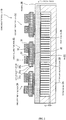
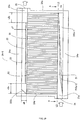
- FIG. 11 is a plan view illustrating the shape of the water jacket used in the cooling device for a semiconductor module in accordance with the present invention.
- the water jacket 2A of type Fc shown in the figure is used as the cooling device 2 of the semiconductor module 10A shown in FIG. 6(A) . Therefore, in the water jacket 2A of type Fc, the introducing port 24 and the discharge port 25 are disposed in the left wall 2Ab, in the same manner as in the water jacket of the conventional type A shown in FIG. 6(B) .
- the introducing port section 21a that introduces the coolant from the introducing port 24 into the coolant introducing flow channel 21, and the discharge port section 22a for allowing the coolant to flow out of the coolant discharge flow channel 22 into the discharge port 25 are formed to be longer than those in the configuration shown in FIG. 6(B) or FIG. 3 .
- the introducing port section 21a and the discharge port section 22a are formed such as to protrude from the same left wall 2Ab.
- the length x of the coolant introducing flow channel 21 is 255.2 mm, and the guide section 21Si provided with a surface inclined at about 45° is formed in the terminating end portion of the coolant introducing flow channel at the inner surface side of the front wall 2Aa that faces the front side surface (coolant inflow surface) of the fins 2C disposed in the flow channel 23 for cooling.
- a gap y between the fins 2C and the guide section 21Si in the terminating end portion of the coolant introducing flow channel 21 is 2 mm, that is, the same as in the water jacket 2A ( FIG. 8 ) of type D.
- the flow velocity adjusting plate 28 is disposed at the boundary position of the coolant discharge flow channel 22 and the flow channel 23.
- the guide section 22So provided with a surface inclined at about 45° is disposed in the starting end section on the right wall 2Ad side, similarly to the guide section 21Si of the coolant introducing flow channel 21.
- the guide section 22So provided with a surface inclined at about 45° is disposed in the starting end section on the right wall 2Ad side, similarly to the guide section 21Si of the coolant introducing flow channel 21.
- FIG. 12 is an explanatory drawing illustrating, for each type, the dimensions of the flow velocity adjusting plate in the cooling device for a semiconductor module shown in FIG. 11 .
- the water jackets 2A of type E, type Ea, type Eb, type F, type Fa, and type Fb are explained.
- the water jackets 2A of all types are formed to have the following dimensions: the flow channel widths (w1, w2) of the coolant introducing flow channel 21 and the coolant discharge flow channel 22 are each equal to 15 mm, the width of the flow channel 23 for cooling is 255 mm, the length thereof is 117 mm, the gap y between the guide section 21Si and the fins 2C is 2 mm, and the gap y2 between the flow velocity adjusting plate 28 and the fins 2C is 2 mm.
- the length L and gap x2 are the same as in other types, that is, 175 mm and 0 mm, respectively, but the height h of the flow velocity adjusting plate 28 varies within a range from 9.5 mm to 5.5 mm.
- the gap x2 is also 0 mm and the height h of the flow velocity adjusting plate 28 varies within a range from 9.5 mm to 5.5 mm, but the difference is that the length L thereof is 215 mm and larger than in the water jacket of type E.
- the difference between type Fc shown in FIG. 11 and all other types is that the gap x2 therein is 5 mm, rather than 0 mm.
- the flow velocity distribution in the flow channel 23 for cooling is modified by the introducing port section 21a (see FIG. 8 ) in which, although the surface area of the introducing port 24 is the same, the cross-sectional area decreases continuously in the coolant introduction direction.
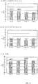
- FIG. 13 shows, for each type, the coolant flow velocity distribution for each position of the circuit substrate, which is the cooling characteristic of the water jacket shown in FIG. 11 .
- the flow velocity distribution shown in the figure is the result obtained by simulating the coolant flow velocity between the fins 2C disposed directly below the central section of the substrate of the circuit element sections 3D to 3I, 3Iu, and 3Id disposed in seven columns (positions B1 to B7).
- the flow velocity is shown from the introducing port 24 side to the positions B1 to B7 toward the terminating end section of the coolant introducing flow channel 21.
- the coolant introducing flow channels 21 used for the simulation of the flow channel distribution are all assumed to have a total length of 255 mm and a height of 10.5 mm.
- the flow velocity distribution changes significantly in the case of type E, type F, and type Fc in which the height of the flow velocity adjusting plate 28 is increased to 9.5 mm. Further, the type E and type F in which the height of the flow velocity adjusting plate 28 is 9.5 mm demonstrate the flow velocity distribution that depends on the length L thereof.
- the flow velocity increases at positions B6 and B7 of the circuit substrate, and in type F, the flow velocity at the position B7 rises especially significantly with respect to that in type Fb.
- any flow velocity distribution can be produced by using the flow velocity adjusting plate 28 inside the coolant discharge flow channel 22, and that even a very small gap of about 5 mm present in the vicinity of the discharge port 25 of the coolant discharge flow channel 22 greatly affects the flow velocity distribution.
- the pressure loss received by the coolant inside the water jacket 2A when the circuit element section 3D is cooled differs among the types shown in FIG. 12 .
- the heat loss inside the water jacket 2A is classified into two groups, each group including three rows from the introducing port 24 side, as shown in the above-described FIG. 6(A) , that is, positions B1 to B3 of the circuit element sections 3D to 3F and the positions B4 to B6 of the circuit element sections 3G to 3I, and it is assumed that in the same group, the heat loss can be set to the same value.
- the heat loss is set to different values in the circuit element section 3Id on the upstream side and the circuit element section 3Iu on the downstream side.
- the objects for comparison of heat generation temperature in FIG. 14 are the IGBT elements disposed on the downstream side of the circuit element section 3D of the first column (position B1) and the circuit element section 3G of the fourth row (position B4). Further, in the seventh column (position B7), the circuit element section (3Id) on the upstream side, which has a higher generation loss, from among the circuit element sections 3Iu and 3Id, is taken as a comparison object. With respect to the generation loss values that are set according to the heat generation amount of each of the circuit element sections 3D to 3I, 3Iu, and 3Id, the relationship 3D ⁇ 3G ⁇ 3Iu ⁇ 3Id is set on the basis of the relationship between the coolant flow velocity, coolant temperature, and cooling performance.
- the junction temperature (Tj) of the circuit element section 3Id is 136.7°C in type E, 134.7°C in type F, and 142.0°C in type Fb in which the flow velocity distribution shifted to the discharge port 25 side.
- the length of the flow velocity adjusting plate 28 ensures a temperature reduction effect equal to or greater than 5°C.
- the junction temperature of each IGBT changes following the changes in the flow velocity distribution downstream of the B1 column and downstream of the B4 column.
- the flow velocity adjusting plate 28 at a boundary position of the coolant discharge flow channel 22 and the flow channel 23 for cooling, it is possible to reduce the junction temperature of the power semiconductor element.
- a particularly significant effect is demonstrated in increasing the flow velocity immediately below the central section of the substrate (position B7) of the circuit element section 3Id with a high generation loss.
- FIG. 15 shows, for each type, the difference in pressure loss between the introducing port and the discharge port when the coolant flows in the semiconductor module shown in FIG. 11 .
- a value less than 4.5 kPa is obtained for all types.
- the pressure loss is decreased in comparison with that of the modification example (type D) on the coolant introducing flow channel 21 side, as in the fourth comparative example shown in FIG. 8 , and the flow velocity distributions practically match each other.
- the coolant introducing flow channel 21 is defined by the inner surface of the bottom wall 2Ae of the water jacket and the front side surface of the fins 2C constituting the heat the inner surface of the bottom wall 2Ae and the rear side surface of the fins 2C. Further, the flow velocity of the coolant flowing from the coolant introducing flow channel 21 to the fins 2C is adjusted, as appropriate, by the pressure generated by collision of the coolant flowing out of the fins 2C with the flow velocity adjusting plate 28 disposed in the coolant discharge flow channel 22, and the drift appearing in the coolant flow velocity in the fins 2C can be eliminated. As a result, the semiconductor element disposed on the cooling device 2 can be cooled uniformly and stably, and malfunction or fracture caused by heat generation in the semiconductor element can be reliably prevented.
- the introducing port 24 and the discharge port 25 are disposed in the same surface of the water jacket 2A, and the flow channel shape can be configured such as to obtain the cooling performance corresponding to generation loss in the different circuit element sections 3D to 31, 3Iu, and 3Id.
- the water jacket 2A with a smaller length from the introducing port 24 to the discharge port 25 can be manufactured easily and stably.
- the front side surfaces are substantially parallel to the inflow direction of the coolant flowing in from the introducing port 24, and the fins are installed at positions flush with the inner wall of the introducing port section 21a, so as not to block the flow of the coolant in the coolant introducing flow channel 21.
- the fin base 2B is at a constant distance from the bottom wall 2Ae of the water jacket 2A, this distance determining the height of the coolant introducing flow channel 21.
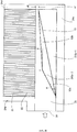
- FIG. 16 is a plan view illustrating the shape of the water jacket used in another cooling device for a semiconductor module in accordance with the present invention.
- a cooling device is explained in which the flow velocity adjusting plate 28 is disposed inside the coolant discharge flow channel 22 and also the length of the flow velocity adjusting plate is made equal to that of the coolant discharge flow channel 22, thereby adjusting the drift in the semiconductor module and cooling the semiconductor element uniformly and stably.
- the introducing port section 21a that guides the coolant from the introducing port 24 into the coolant introducing flow channel 21, and the discharge port section 22a for allowing the coolant to flow out from the coolant discharge flow channel 22 into the discharge port 25 are formed to protrude from the same left wall 2Ab of the water jacket 2A.
- the flow velocity adjusting plate 28 with a length equal to the length x of the coolant discharge flow channel 22 is disposed at a boundary position of the coolant discharge flow channel 22 and the flow channel 23 for cooling.
- FIG. 17 is an explanatory drawing showing, for each type, the dimensions of the flow velocity adjusting plate and the flow channel width in the introducing port and discharge port in the cooling device for a semiconductor module shown in FIG. 16 .
- the flow velocity adjusting plate 28 is formed at any height not exceeding 8 mm in the vertical direction from the surface of the bottom wall 2Ae of the water jacket 2A.
- the flow channel 23 for cooling is configured between the coolant introducing flow channel 21 with a width of 10 mm and the coolant discharge flow channel 22 with a width of 15 mm.
- this figure shows also the dimensions relating to type Ga, type Gb, type Gc, type H, and type I.
- the flow velocity of the coolant flowing in the flow channel 23 for cooling has a flow velocity distribution depending on the position of the discharge port 25 of the water jacket 2A.
- the water jacket 2A of type G is different from the water jackets of type E and type F shown in FIG. 12 in that the length of the flow velocity adjusting plate 28 is made equal to the length x of the coolant discharge flow channel 22 (that is, the width of the flow channel 23 for cooling), and the flow velocity adjusting plate 28 is connected to the left wall 2Ab (side wall of the flow channel 23 for cooling on the discharge port 25 side) of the water jacket 2A.
- FIG. 18(A) shows, for each type, the coolant flow velocity distribution at each position of the circuit substrate, which is the cooling characteristic of the water jacket shown in FIG. 16
- FIG. 18(B) shows, for each type, the difference in pressure loss between the introducing port and the discharge port.
- the flow velocity distribution shown in FIG. 18(A) is obtained by simulation immediately below the central section of the substrate of the circuit element sections 3D to 3I, 3Iu, and 3Id disposed at the circuit substrate positions B1 to B7 shown in FIG. 6(A) , and the coolant flow velocity distribution is compared among the types for each position B1 to B7.
- the difference in pressure loss is the difference in pressure between the introducing port 24 and the discharge port 25.
- the simulation results are shown that relate to type G, type Ga, type Gb, type Gc, type H, and type I. It is clear that in types G, Ga, Gb, Gc in which the flow velocity adjusting plate 28 is disposed at different heights h of 2 mm, 4 mm, 6 mm, and 8 mm, respectively, in the coolant introducing flow channel 21 with a flow channel width W1 of 10 mm, the coolant flow velocity is particularly reduced at the circuit substrate position B7, thereby enabling the adjustment to a uniform flow velocity distribution.
- the difference between the highest flow velocity and the lowest flow velocity is the smallest when the difference between the flow channel width W1 of the coolant introducing flow channel 21 and the flow channel width W2 of the coolant discharge flow channel 22 is 2.5 mm (type I).
- the best uniformity of the flow velocity distribution is realized.
- the difference in pressure is 5.2 kPa, and the variation of pressure loss depends on the width W1 of the coolant introducing flow channel 21. This result indicates that the uniformity of coolant flow velocity distribution is in a trade-off relationship with the difference in pressure loss.
- the uniformity of drift distribution can be improved by making the length of the flow velocity adjusting plate 28 equal to that of the coolant discharge flow channel 22 and reducing to a certain degree the flow channel width w1 of the coolant introducing flow channel 21.
- Described below is an embodiment in which a plurality of guide sections are provided in the coolant introducing flow channel and the adjustment of flow velocity distribution in the flow channels for cooling constituted by a plurality of rows is performed more effectively.
- FIG. 19 illustrates a configuration example of a water jacket for use in a cooling device for a semiconductor module.
- the water jacket 2A-0 for use in a cooling device for a semiconductor module has a substantially rectangular parallelepiped shape.
- the water jacket 2A-0 is provided with a coolant introducing flow channel 21, an introducing port section 21a, a coolant discharge flow channel 22, a discharge port section 22a, and a flow channel 23 for cooling that has the fins 2C disposed therein.
- Those coolant introducing flow channel 21 and the like are defined by a front wall 2Aa, a left wall 2Ab, a rear wall 2Ac, a right wall 2Ad, and the water jacket 2A-0.
- the fins 2C are depicted in the drawing for the sake of convenience of explanation.
- an introducing port 24 for introducing the coolant into the water jacket and a discharge port 25 for discharging the coolant therefrom are arranged such that the discharge port 25 is formed at a position diagonally opposite the introducing port 24 in the water jacket 2A-0.
- the introducing port 24 is provided in the lower section of the left wall 2Ab of the water jacket 2A-0
- the discharge port 25 is provided in the upper section of the right wall 2Ad (a configuration may be also used in which the introducing port 24 is provided in the upper section of the left wall 2Ab, and the discharge port 25 is provided in the lower section of the right wall 2Ad).
- the coolant introduction direction in the introducing port 24 and the coolant discharge direction in the discharge port 25 are oriented in the same direction.
- a flow velocity adjusting plate 28 is provided in a substantially central section of the coolant discharge flow channel 22 at a boundary position of the coolant discharge flow channel 22 and the flow channel 23 for cooling.
- the flow velocity adjusting plate 28 is disposed such that the side wall surface thereof is parallel to the coolant outflow surface of the fins 2C, with a gap y2 being formed therebetween, a gap x2a is formed between one end of the flow velocity adjusting plate and the side surface of the left wall 2Ab, and a gap x2b is formed between the other end of the flow velocity adjusting plate and the side surface of the right wall 2Ad.
- the starting end section of the coolant discharge flow channel 22 through which the coolant flows out to the discharge port 25 is chamfered to form a guide section 22So having an inclination angle of about 45°.
- Guide sections 21So-1, 21So-2 are additionally provided inside the coolant introducing flow channel 21.
- FIG. 20 shows a configuration example of the guide sections. This figure is an enlarged view of the guide sections 21So-1 and 21So-2 configured as shown in FIG. 19 and the surroundings thereof.
- the guide section 21So-1 has a guide wall S1 on the surface facing the flow channel 23 for cooling, and the surface on the side opposite that of the guide wall S1 is in contact with the front wall 2Aa.
- the guide wall S1 of the guide section 21So-1 is inclined such that the introducing flow channel cross-section area of the coolant introducing flow channel 21 decreases from the introducing port 24 toward an abutment wall a1 inside the coolant introducing flow channel 21.
- the guide section 21So-2 has guide walls S2a, S2b on the surface facing the flow channel 23 for cooling, and the surface of this guide section on the side opposite that of the guide walls S2a, S2b is in contact with the guide wall S1 of the guide section 21So-1.
- the guide walls S2a, S2b of the guide section 21So-2 are formed with an inflection point P as a boundary.
- the guide wall S2a is inclined such that the introducing flow channel cross-section area of the coolant introducing flow channel 21 decreases from the introducing port 24 toward the inflection point P.
- the guide wall S2b is inclined such that the introducing flow channel cross-section area of the coolant introducing flow channel 21 decreases from the inflection point P toward the abutment wall a1 inside the coolant introducing flow channel 21.
- An angle between a straight line in the longitudinal direction of the coolant introducing flow channel 21 and the guide wall S2a is taken as an inclination angle ⁇
- an angle between a straight line in the longitudinal direction of the coolant introducing flow channel 21 and the guide wall S2b is taken as an inclination angle ⁇ .
- ⁇ ⁇ ⁇ that is, the inclination angle ⁇ of the guide wall S2a is larger than the inclination angle ⁇ of the guide wall S2b.
- the fins 2C and the guide wall S2b form a gap (minimum value) y0 at the abutment wall a1.
- FIG. 21 is a cross-sectional view taken along the L2-L2 line.
- the cross section taken along the L2-L2 line shown in FIG. 19 is viewed from the direction of arrow A.
- the height of the guide section 21So-1 above the bottom surface of the coolant introducing flow channel 21, that is, the height of the guide wall S1 is taken as h1.
- the height of the guide section 21So-2 which is positioned in front of the guide section 21So-1, above the bottom surface of the coolant introducing flow channel 21, that is, the height of the guide walls S2a, S2b, is taken as h2. In this case, the relationship h2 ⁇ h1 is satisfied.
- the heights h1, h2 can be such that the height h2 of the guide walls S2a, S2b is taken as about half of the length of the fins 2C from the bottom surface of the coolant introducing flow channel 21, and the height h1 of the guide wall S1 is taken as a length from the bottom surface of the coolant introducing flow channel 21 to the mounting surface of the fins 2C of the base material 26 ( FIG. 2 ).
- Described above is the configuration in which the guide sections 21So-1, 21So-2 are provided as two guide sections inside the coolant introducing flow channel 21, and the guide section 21So-1 is higher than the guide section 21So-2.
- the side surface (corresponds to the guide wall S1) of the guide section (corresponds to the guide section 21So-1) that is in contact with the front wall 2Aa of the water jacket 2A-0 is made the highest among the plurality of guide sections.
- the height of the side surface of the guide sections is decreased with the transition from the guide section that is in contact with the front wall 2Aa to the guide section at a position that is closer to the flow channel 23 for cooling.
- the height of the guide wall of the guide section that is in contact with the front wall 2Aa of the water jacket 2A-0 inside the coolant introducing flow channel 21 is made the largest, the height of the guide wall is set lower for a guide section disposed farther from the front wall 2Aa and closer to the flow channel 23 for cooling, and the height of the plurality of guide sections inside the coolant introducing flow channel 21 is formed in a stepwise manner.
- the introducing port 24 for introducing the coolant into the water jacket and the discharge port 25 for discharging the coolant to the outside are provided at mutually symmetrical positions in the water jacket 2A-0, and the guide sections 21So-1, 21So-2 are not present.
- the guide section 21So-1 by providing such a configuration with the guide section 21So-1, it is possible to intensify the coolant flow at the introducing port 24 side. Therefore, the phenomenon of the coolant flow velocity distribution inside the flow channel 23 becoming intensively higher at the discharge port 25 side can be suppressed.
- the guide section 21So-2 is additionally provided, the coolant flow at the introducing port 24 side can be further increased.
- the heat generation distribution of the circuit elements mounted on the base material 26 is taken into account, in the case in which the circuit element sections with a high loss density and high heat generation ability are mounted on the circumferential portion of the introducing port 24 and the circumferential portion of the discharge port 25 at the base material 26 and the circuit element section with a low loss density and low heat generation ability is mounted in the central portion of the base material 26, the water jacket 2A-0, which has the guide sections 21So-1 and 21So-2, can cool those circuit element sections effectively.
- FIG. 22 shows the water jacket of one embodiment. Only the features different from those illustrated by FIG. 19 will be mainly explained below.
- the introducing port 24 and the discharge port 25 of the water jacket 2A-1 are provided at the same side surface.
- the introducing port 24 is provided in the lower portion of the left wall 2Ab of the water jacket 2A-1, and the discharge port 25 is provided in the upper portion of the left wall 2Ab.
- the coolant introduction direction in the introducing port 24 is opposite to the coolant discharge direction in the discharge port 25.
- a flow velocity adjusting plate 28-1 is disposed in the coolant discharge flow channel 22 closer to the discharge port 25 at the boundary position of the coolant discharge flow channel 22 and the flow channel 23 for cooling, and a flow velocity adjusting plate 28-2 is disposed adjacently to the flow velocity adjusting plate 28-1 in a substantially central portion of the coolant discharge flow channel 22.
- the height ha of the flow velocity adjusting plate 28-1 is about half the length of the fin 2C from the bottom surface of the coolant discharge flow channel 22, and the height hb of the flow velocity adjusting plate 28-2 is substantially the length from the bottom surface of the coolant discharge flow channel 22 to the attachment surface of the fins 2C at the base material 26.
- Other components, such as guide sections, are basically the same as in the configuration shown in FIG. 19 .
- the coolant flow velocity rises at a position close to the left wall 2Ab where the introducing port 24 and the discharge port 25 are disposed, and the coolant flow velocity also rises at a position close to the right wall 2Ad.
- the rise of the coolant flow velocity in a substantially central portion of the flow channel 23 for cooling is suppressed.
- the configuration is used such that the introducing port 24 and the discharge port 25 are provided at the same side surface, a plurality of guide sections 21So-1, 21So-2 are provided inside the coolant introducing flow channel 21, and the flow velocity adjusting plates 28-1, 28-2 of different height are disposed at the boundary position of the coolant discharge flow channel 22 and the flow channel 23 for cooling.
- the flow velocity distribution of the coolant flowing in the flow channel 23 for cooling at a position close to one wall side where the introducing port 24 and the discharge port 25 are disposed is raised, and the flow velocity distribution of the coolant flowing in the flow channel 23 for cooling at a position close to the other wall side where the introducing port 24 and the discharge port 25 are not disposed is also raised.
- the increase in coolant flow velocity is inhibited.
- FIG. 23 shows a variation example of the water jacket. Only the features different from those illustrated by FIG. 19 will be mainly explained below.
- the introducing port 24 and the discharge port 25 of the water jacket 2A-2 are arranged such that the discharge port 25 is formed at a position diagonally opposite to the position of the introducing port 24 in the water jacket 2A-2.
- the introducing port 24 is provided in the lower portion of the left wall 2Ab of the water jacket 2A-2
- the discharge port 25 is provided in the upper portion of the right wall 2Ad
- the coolant introduction direction of the introducing port 24 is at a right angle with respect to the coolant discharge direction of the discharge port 25.
- Other components such as a flow velocity adjusting plate and guide sections are basically the same as in the configuration shown in FIG. 19 .
- the introducing port 24 and the discharge port 25 are provided at symmetrical positions, and the coolant introduction direction in the introducing port 24 and the coolant discharge direction in the discharge port 25 are oriented such as to be at a right angle with respect to each other. Further, a configuration is used in which the plurality of guide sections 21So-1, 21So-2 are provided inside the coolant introducing flow channel 21, and the flow velocity adjusting plate 28 is disposed at the boundary position of the coolant discharge flow channel 22 and the flow channel 23 for cooling.
- the flow velocity distribution of the coolant flowing in the flow channel 23 for cooling at a position close to one wall side where the introducing port 24 is disposed is raised, and the flow velocity distribution of the coolant flowing in the flow channel 23 for cooling at a position close to the other wall side where the discharge port 25 is disposed is also raised. Further, in a substantially central portion of the flow channel 23 for cooling, the increase in coolant flow velocity is inhibited.
- the width of the coolant introducing flow channel 21 is denoted by wa and the width of the coolant discharge flow channel 22 is denoted by wb.
- wa ⁇ wb it is preferred that the water jacket 2A-0 shown in FIG. 19 be used.
- wa ⁇ wb it is preferred that the water jacket 2A-2 shown in FIG. 23 be used.
Landscapes
- Engineering & Computer Science (AREA)
- Physics & Mathematics (AREA)
- Thermal Sciences (AREA)
- Mechanical Engineering (AREA)
- General Engineering & Computer Science (AREA)
- Microelectronics & Electronic Packaging (AREA)
- Cooling Or The Like Of Semiconductors Or Solid State Devices (AREA)
- Cooling Or The Like Of Electrical Apparatus (AREA)
- Chemical & Material Sciences (AREA)
- Ceramic Engineering (AREA)
Claims (14)
- Dispositif de refroidissement (2) pour un module à semi-conducteurs qui est capable de fournir un fluide de refroidissement à partir de l'extérieur dans une chemise d'eau (2A) et capable de refroidir un élément semi-conducteur à disposer sur une surface extérieure de celui-ci, le dispositif de refroidissement (2) comprenant :des moyens de dissipation de chaleur (2C) reliés thermiquement à l'élément semi-conducteur ;des premiers moyens formant canal d'écoulement (21) disposés à l'intérieur de la chemise d'eau (2A), s'étendant d'un orifice d'introduction de fluide de refroidissement (24), et dans lesquels des moyens de guidage (21Si) qui ont une surface inclinée pour guider le fluide de refroidissement vers une surface latérale des moyens de dissipation de chaleur (2C) sont disposés ;des deuxièmes moyens formant canal d'écoulement (22) disposés à l'intérieur de la chemise d'eau (2A) parallèlement aux premiers moyens formant canal d'écoulement (21) à une distance de ceux-ci, s'étendant vers l'orifice de décharge de fluide de refroidissement (25), et dans lesquels une paroi latérale parallèle à une autre surface latérale des moyens de dissipation de chaleur (2C) est formée ; etdes troisièmes moyens formant canal d'écoulement (23) formés à une position mettant en communication les premiers moyens formant canal d'écoulement (21) et les deuxièmes moyens formant canal d'écoulement (22) à l'intérieur de la chemise d'eau (2A), dans lequelles moyens de dissipation de chaleur (2C) sont disposés dans les troisièmes moyens formant canal d'écoulement (23),caractérisé pardes moyens d'ajustement de vitesse d'écoulement (28) disposés dans les deuxièmes moyens formant canal d'écoulement (22) et formés parallèlement à l'autre surface latérale des moyens de dissipation de chaleur (2C) à une distance de ceux-ci ;dans lequel l'orifice d'introduction de fluide de refroidissement (24) et l'orifice de décharge de fluide de refroidissement (25) sont formés dans la même surface de paroi de la chemise d'eau (2A).
- Dispositif de refroidissement (2) pour un module à semi-conducteurs selon la revendication 1, dans lequel les moyens d'ajustement de vitesse d'écoulement (28) sont disposés de sorte qu'une section d'extrémité de ceux-ci soit positionnée dans une section d'extrémité de terminaison des deuxièmes moyens formant canal d'écoulement (22), et également de manière à s'étendre parallèlement aux moyens de dissipation de chaleur (2C) à une distance de l'autre surface latérale des moyens de dissipation de chaleur (2C).
- Dispositif de refroidissement (2) pour un module à semi-conducteurs selon la revendication 1, dans lequel les moyens d'ajustement de vitesse d'écoulement (28) sont disposés de sorte qu'une section d'extrémité de ceux-ci soit positionnée à une distance prédéterminée d'une section d'extrémité de terminaison des deuxièmes moyens formant canal d'écoulement (22) du côté d'orifice de décharge de fluide de refroidissement des deuxièmes moyens formant canal d'écoulement (22), et également de manière à s'étendre parallèlement aux moyens de dissipation de chaleur (2C) à une distance de l'autre surface latérale des moyens de dissipation de chaleur (2C).
- Dispositif de refroidissement (2) pour un module à semi-conducteurs selon la revendication 2, dans lequel les moyens d'ajustement de vitesse d'écoulement (28) sont disposés de sorte que l'autre section d'extrémité de ceux-ci soit à une distance supérieure ou égale à 0,05x des moyens de guidage (22So) formés dans une section d'extrémité de début des deuxièmes moyens formant canal d'écoulement (22), où x est une longueur des deuxièmes moyens formant canal d'écoulement (22).
- Dispositif de refroidissement (2) pour un module à semi-conducteurs selon la revendication 2, dans lequel les moyens d'ajustement de vitesse d'écoulement (28) sont formés à une hauteur de 0,2h inclus à 0,9h inclus par rapport à une surface inférieure de la chemise d'eau (2A), où h est une hauteur des deuxièmes moyens formant canal d'écoulement.
- Dispositif de refroidissement (2) pour un module à semi-conducteurs selon la revendication 1, dans lequel les moyens d'ajustement de vitesse d'écoulement (28) ont une longueur égale à une longueur des deuxièmes moyens formant canal d'écoulement et sont formés à une hauteur de 0,2h inclus à 0,9h inclus par rapport à une surface inférieure de la chemise d'eau (2A), où h est une hauteur des deuxièmes moyens formant canal d'écoulement.
- Module à semi-conducteurs dans lequel un fluide de refroidissement peut être fourni à partir de l'extérieur dans une chemise d'eau constituant un dispositif de refroidissement qui est capable de refroidir un élément semi-conducteur à disposer sur une surface extérieure du dispositif de refroidissement, le module à semi-conducteurs comprenant ledit dispositif de refroidissement (2) selon l'une quelconque des revendications précédentes.
- Dispositif de refroidissement (2) pour un module à semi-conducteurs selon l'une quelconque des revendications 1 à 6, le dispositif de refroidissement (2) comprenant :
les premiers moyens formant canal d'écoulement (21) disposés à l'intérieur de la chemise d'eau (2A), s'étendant de l'orifice d'introduction de fluide de refroidissement (24), et dans lesquels une pluralité de moyens de guidage (21So-1, 21So-2) qui ont des surfaces inclinées mutuellement différentes pour guider le fluide de refroidissement vers une surface latérale des moyens de dissipation de chaleur (2C) sont disposés. - Dispositif de refroidissement (2) pour un module à semi-conducteurs selon la revendication 8, dans lequel la pluralité de moyens de guidage (21So-1, 21So-2) sont à des hauteurs mutuellement différentes par rapport à une surface inférieure des premiers moyens formant canal d'écoulement et chacun des moyens de guidage (21So-1, 21So-2) a sa propre surface inclinée.
- Dispositif de refroidissement (2) pour un module à semi-conducteurs selon la revendication 9, dans lequel la pluralité de moyens de guidage (21So-1, 21So-2) sont formés de sorte que la hauteur des moyens de guidage (21So-1, 21So-2) qui est en contact avec une surface latérale de la chemise d'eau (2A) soit la plus grande, et les moyens de guidage (21So-1, 21So-2) disposés à une position plus proche des troisièmes moyens formant canal d'écoulement (23) ont une plus petite hauteur, et sont formés de manière étagée par rapport à la surface inférieure des premiers moyens formant canal d'écoulement (21).
- Dispositif de refroidissement (2) pour un module à semi-conducteurs selon la revendication 8, dans lequel les surfaces inclinées de la pluralité de moyens de guidage (21So-1, 21So-2) sont formées de sorte que la section des premiers moyens formant canal d'écoulement (21) diminue dans la direction d'extension de l'orifice d'introduction de fluide de refroidissement (24).
- Dispositif de refroidissement (2) pour un module à semi-conducteurs selon la revendication 8, dans lequel la pluralité de moyens de guidage (21So-1, 21So-2) comprennent des premiers moyens de guidage qui sont en contact avec une surface latérale de la chemise d'eau (2A) et des deuxièmes moyens de guidage qui sont en contact avec les premiers moyens de guidage sur une plage faisant face aux troisièmes moyens formant canal d'écoulement (23), et la pluralité de moyens de guidage (21So-1, 21So-2) sont formés de sorte que la hauteur des premiers moyens de guidage soit supérieure à la hauteur des deuxièmes moyens de guidage.
- Dispositif de refroidissement pour un module à semi-conducteurs selon la revendication 12, dans lequel
la surface inclinée des premiers moyens de guidage a une inclinaison uniforme par rapport à la plage faisant face aux troisièmes moyens formant canal d'écoulement (23) et est formée de sorte que la section des premiers moyens formant canal d'écoulement (21) diminue dans la direction d'extension de l'orifice d'introduction de fluide de refroidissement (24), et
la surface inclinée des deuxièmes moyens de guidage a une pluralité d'inclinaisons différentes par rapport à la plage faisant face aux troisièmes moyens formant canal d'écoulement et est formée de sorte que la section des premiers moyens formant canal d'écoulement (21) diminue dans la direction d'extension de l'orifice d'introduction de fluide de refroidissement (24). - Module à semi-conducteurs dans lequel un fluide de refroidissement peut être fourni à partir de l'extérieur dans une chemise d'eau constituant un dispositif de refroidissement qui est capable de refroidir un élément semi-conducteur à disposer sur une surface extérieure du dispositif de refroidissement, le module à semi-conducteurs comprenant ledit dispositif de refroidissement, étant un dispositif de refroidissement selon l'une quelconque des revendications 8 à 13,
dans lequel
l'orifice d'introduction de fluide de refroidissement (24) et l'orifice de décharge de fluide de refroidissement (25) sont formés dans la même surface de paroi de la chemise d'eau (2A), ou l'orifice de décharge de fluide de refroidissement est formé à une position qui est opposée en diagonale à la position de l'orifice d'introduction de fluide de refroidissement (24) dans la chemise d'eau (2A).
Applications Claiming Priority (3)
| Application Number | Priority Date | Filing Date | Title |
|---|---|---|---|
| JP2011224469 | 2011-10-12 | ||
| PCT/JP2012/072554 WO2013054615A1 (fr) | 2011-10-12 | 2012-09-05 | Refroidisseur pour module à semi-conducteurs, et module à semi-conducteurs |
| PCT/JP2012/076453 WO2013054887A1 (fr) | 2011-10-12 | 2012-10-12 | Refroidisseur pour module à semiconducteur, et module à semiconducteur |
Publications (3)
| Publication Number | Publication Date |
|---|---|
| EP2768018A1 EP2768018A1 (fr) | 2014-08-20 |
| EP2768018A4 EP2768018A4 (fr) | 2015-07-01 |
| EP2768018B1 true EP2768018B1 (fr) | 2020-02-26 |
Family
ID=48081674
Family Applications (2)
| Application Number | Title | Priority Date | Filing Date |
|---|---|---|---|
| EP12839733.8A Active EP2768017B1 (fr) | 2011-10-12 | 2012-09-05 | Refroidisseur pour module à semi-conducteurs, et module à semi-conducteurs |
| EP12839889.8A Active EP2768018B1 (fr) | 2011-10-12 | 2012-10-12 | Refroidisseur pour module à semiconducteur, et module à semiconducteur |
Family Applications Before (1)
| Application Number | Title | Priority Date | Filing Date |
|---|---|---|---|
| EP12839733.8A Active EP2768017B1 (fr) | 2011-10-12 | 2012-09-05 | Refroidisseur pour module à semi-conducteurs, et module à semi-conducteurs |
Country Status (6)
| Country | Link |
|---|---|
| US (2) | US9293391B2 (fr) |
| EP (2) | EP2768017B1 (fr) |
| JP (2) | JP5900506B2 (fr) |
| KR (2) | KR101906645B1 (fr) |
| CN (2) | CN103890938B (fr) |
| WO (2) | WO2013054615A1 (fr) |
Families Citing this family (58)
| Publication number | Priority date | Publication date | Assignee | Title |
|---|---|---|---|---|
| JP5343007B2 (ja) * | 2007-11-26 | 2013-11-13 | 株式会社豊田自動織機 | 液冷式冷却装置 |
| CN103890938B (zh) | 2011-10-12 | 2017-10-13 | 富士电机株式会社 | 半导体模块用冷却器及半导体模块 |
| JP5900610B2 (ja) * | 2012-04-16 | 2016-04-06 | 富士電機株式会社 | 半導体装置および半導体装置用冷却器 |
| WO2014020808A1 (fr) * | 2012-08-03 | 2014-02-06 | 富士電機株式会社 | Structure de refroidissement et convertisseur d'énergie |
| JP5975110B2 (ja) * | 2012-10-29 | 2016-08-23 | 富士電機株式会社 | 半導体装置 |
| JP6086033B2 (ja) * | 2013-06-05 | 2017-03-01 | 株式会社豊田自動織機 | インバータ装置 |
| JP6168152B2 (ja) * | 2013-09-05 | 2017-07-26 | 富士電機株式会社 | 電力用半導体モジュール |
| JP6164304B2 (ja) * | 2013-11-28 | 2017-07-19 | 富士電機株式会社 | 半導体モジュール用冷却器の製造方法、半導体モジュール用冷却器、半導体モジュール及び電気駆動車両 |
| EP3032580B1 (fr) * | 2014-03-14 | 2018-06-20 | Fuji Electric Co., Ltd. | Dispositif de refroidissement et dispositif à semi-conducteurs comportant ledit dispositif de refroidissement |
| US9960100B2 (en) | 2014-03-20 | 2018-05-01 | Fuji Electric Co., Ltd | Cooler and semiconductor module using same |
| JP6098760B2 (ja) * | 2014-05-20 | 2017-03-22 | 富士電機株式会社 | 半導体モジュール用冷却器及びその製造方法 |
| JP6316096B2 (ja) * | 2014-05-28 | 2018-04-25 | 昭和電工株式会社 | 液冷式冷却装置 |
| KR102291151B1 (ko) * | 2014-11-03 | 2021-08-19 | 현대모비스 주식회사 | 전력변환장치용 냉각유로모듈 및 이를 구비한 전력변화장치 |
| CN105841403A (zh) * | 2015-01-12 | 2016-08-10 | 杭州三花研究院有限公司 | 冷却装置 |
| CN104754921B (zh) * | 2015-03-06 | 2018-03-06 | 西安电子科技大学 | 热源面温度均匀的微通道散热器 |
| JP6477276B2 (ja) * | 2015-06-12 | 2019-03-06 | 富士通株式会社 | クーリングプレート及びクーリングプレートを備える情報処理装置 |
| WO2016203885A1 (fr) * | 2015-06-17 | 2016-12-22 | 富士電機株式会社 | Module semiconducteur de puissance et refroidisseur |
| FR3049159B1 (fr) * | 2016-03-15 | 2019-10-25 | Institut Vedecom | Module d’electronique de puissance refroidi, moteur et vehicule integrant un tel module |
| KR101848152B1 (ko) * | 2016-09-06 | 2018-04-12 | 황의수 | 복수 열전소자용 소형냉각장치 |
| KR101848151B1 (ko) * | 2016-09-06 | 2018-04-12 | 황의수 | 소형냉각장치 |
| US11284534B2 (en) * | 2016-09-23 | 2022-03-22 | Sumitomo Precision Products Co., Ltd. | Cooling device |
| US10136564B2 (en) * | 2016-09-30 | 2018-11-20 | Denso Corporation | Power converter |
| CN106714511A (zh) * | 2016-11-29 | 2017-05-24 | 洛阳新巨能高热技术有限公司 | 新型水冷散热器 |
| CN106535572A (zh) * | 2016-11-29 | 2017-03-22 | 洛阳新巨能高热技术有限公司 | 一种新型水冷散热器 |
| CN106535573A (zh) * | 2016-11-29 | 2017-03-22 | 洛阳新巨能高热技术有限公司 | 水冷散热器 |
| CN106793677A (zh) * | 2016-11-29 | 2017-05-31 | 洛阳新巨能高热技术有限公司 | 一种水冷散热器 |
| WO2018116653A1 (fr) * | 2016-12-20 | 2018-06-28 | 富士電機株式会社 | Module semi-conducteur |
| JP6880776B2 (ja) * | 2017-01-27 | 2021-06-02 | 株式会社デンソー | 電力変換装置 |
| DE102018112601A1 (de) * | 2017-05-31 | 2018-12-06 | Hanon Systems | Elektroelement-Kühlungsmodul |
| JP6636996B2 (ja) * | 2017-07-11 | 2020-01-29 | ファナック株式会社 | Ldモジュール冷却装置及びレーザ装置 |
| US10292316B2 (en) * | 2017-09-08 | 2019-05-14 | Hamilton Sundstrand Corporation | Power module with integrated liquid cooling |
| JP7205071B2 (ja) | 2018-04-02 | 2023-01-17 | 富士電機株式会社 | 冷却装置、半導体モジュールおよび車両 |
| US10665525B2 (en) * | 2018-05-01 | 2020-05-26 | Semiconductor Components Industries, Llc | Heat transfer for power modules |
| JP7124425B2 (ja) | 2018-05-02 | 2022-08-24 | 富士電機株式会社 | 冷却装置、半導体モジュールおよび車両 |
| DE102018112000B4 (de) * | 2018-05-18 | 2024-08-08 | Rogers Germany Gmbh | System zum Kühlen eines Metall-Keramik-Substrats, ein Metall-Keramik-Substrat und Verfahren zum Herstellen des Systems |
| JP7087850B2 (ja) * | 2018-09-05 | 2022-06-21 | 株式会社デンソー | 半導体装置 |
| DE102018215142A1 (de) * | 2018-09-06 | 2020-03-12 | Robert Bosch Gmbh | Sensoreinheit eines Fahrzeugs |
| US11129310B2 (en) * | 2018-11-22 | 2021-09-21 | Fuji Electric Co., Ltd. | Semiconductor module, vehicle and manufacturing method |
| WO2020174584A1 (fr) | 2019-02-26 | 2020-09-03 | 三菱電機株式会社 | Dispositif à semi-conducteur, procédé de fabrication de dispositif à semi-conducteur et dispositif de conversion de puissance |
| CN114207812B (zh) * | 2019-07-25 | 2024-12-20 | 日立能源有限公司 | 包括冷却器和用于功率半导体模块的基板的装置 |
| JP7367418B2 (ja) * | 2019-09-13 | 2023-10-24 | 富士電機株式会社 | 半導体モジュールおよび車両 |
| KR102328940B1 (ko) * | 2019-12-13 | 2021-11-19 | 한국전자기술연구원 | 핀휜 구조 히트싱크의 균일 냉각성을 향상시키기 위한 수냉각 장치 구조 |
| TWI738602B (zh) * | 2020-01-22 | 2021-09-01 | 訊凱國際股份有限公司 | 多通道薄熱交換器 |
| JP7229195B2 (ja) * | 2020-03-10 | 2023-02-27 | 三菱電機株式会社 | 発熱素子冷却装置 |
| CN111447805A (zh) * | 2020-05-11 | 2020-07-24 | 珠海格力电器股份有限公司 | 散热效率高的散热组件、电器盒及空调 |
| JP2021190665A (ja) * | 2020-06-04 | 2021-12-13 | 三井化学株式会社 | 冷却装置 |
| CN212084987U (zh) * | 2020-07-09 | 2020-12-04 | 宁波市哈雷换热设备有限公司 | 一种承压能力强的芯片冷却器 |
| JP6961047B1 (ja) * | 2020-07-17 | 2021-11-05 | 三菱電機株式会社 | 電力変換装置 |
| JP6921282B1 (ja) * | 2020-07-17 | 2021-08-18 | 三菱電機株式会社 | 電力変換装置 |
| US11502349B2 (en) * | 2020-08-31 | 2022-11-15 | Borgwarner, Inc. | Cooling manifold assembly |
| JP7577948B2 (ja) * | 2020-09-15 | 2024-11-06 | 富士電機株式会社 | 冷却器及び半導体装置 |
| KR102590521B1 (ko) * | 2021-06-23 | 2023-10-17 | 중앙대학교 산학협력단 | 반도체 패키징 |
| JP7333874B1 (ja) * | 2021-10-11 | 2023-08-25 | 東芝三菱電機産業システム株式会社 | 電気機器 |
| WO2024034291A1 (fr) * | 2022-08-08 | 2024-02-15 | 富士電機株式会社 | Refroidisseur et dispositif semi-conducteur |
| JP7773453B2 (ja) * | 2022-09-26 | 2025-11-19 | 株式会社日立製作所 | 電力変換装置 |
| US12363860B2 (en) | 2023-04-14 | 2025-07-15 | International Business Machines Corporation | Isolating temperature fluctuation in an electronics enclosure |
| KR102923440B1 (ko) | 2024-11-27 | 2026-02-05 | 주식회사 엠디엠 | 냉각유로 삽입형 반도체 패키지 모듈 |
| US12513855B1 (en) * | 2025-03-07 | 2025-12-30 | Adeia Semiconductor Bonding Technologies Inc. | Integrated cooling assembly with upper and lower channels |
Family Cites Families (29)
| Publication number | Priority date | Publication date | Assignee | Title |
|---|---|---|---|---|
| US2934322A (en) * | 1955-09-01 | 1960-04-26 | Frederick E Hazard | Heat exchanger |
| DE19514544A1 (de) * | 1995-04-20 | 1996-10-24 | Daimler Benz Ag | Mikrokühleinrichtung |
| DE19514545A1 (de) | 1995-04-20 | 1996-10-24 | Daimler Benz Ag | Anordnung von mehreren mit elektronischen Bauelementen versehenen Mikrokühleinrichtungen |
| DE19643717A1 (de) * | 1996-10-23 | 1998-04-30 | Asea Brown Boveri | Flüssigkeits-Kühlvorrichtung für ein Hochleistungshalbleitermodul |
| JP2000340727A (ja) * | 1999-05-26 | 2000-12-08 | Nissan Motor Co Ltd | 電子部品の冷却構造 |
| JP2001035981A (ja) | 1999-07-16 | 2001-02-09 | Toshiba Corp | 半導体素子用冷却器及びこれを用いた電力変換装置 |
| JP2001352025A (ja) * | 2000-06-05 | 2001-12-21 | Toshiba Corp | 発熱体冷却装置 |
| JP2006080211A (ja) | 2004-09-08 | 2006-03-23 | Toyota Motor Corp | 半導体装置 |
| JP2006210819A (ja) | 2005-01-31 | 2006-08-10 | Toyota Motor Corp | 半導体冷却装置 |
| KR100619076B1 (ko) * | 2005-04-11 | 2006-08-31 | 삼성전자주식회사 | 전자소자 방열용 히트싱크장치 |
| JP4608641B2 (ja) | 2005-04-27 | 2011-01-12 | 株式会社豊田自動織機 | パワーモジュール用ヒートシンク |
| JP4699820B2 (ja) | 2005-06-28 | 2011-06-15 | 本田技研工業株式会社 | パワー半導体モジュール |
| JP2007242724A (ja) * | 2006-03-06 | 2007-09-20 | Seiko Epson Corp | マイクロチャンネル構造体、マイクロチャンネル構造体の製造方法及び電子機器 |
| JP4789813B2 (ja) * | 2007-01-11 | 2011-10-12 | トヨタ自動車株式会社 | 半導体素子の冷却構造 |
| JP5332115B2 (ja) | 2007-02-22 | 2013-11-06 | 三菱マテリアル株式会社 | パワー素子搭載用ユニット |
| JP2008235725A (ja) * | 2007-03-23 | 2008-10-02 | Calsonic Kansei Corp | 水冷式ヒートシンク |
| US7564129B2 (en) | 2007-03-30 | 2009-07-21 | Nichicon Corporation | Power semiconductor module, and power semiconductor device having the module mounted therein |
| JP5046378B2 (ja) | 2007-03-30 | 2012-10-10 | ニチコン株式会社 | パワー半導体モジュール、および該モジュールを搭載したパワー半導体デバイス |
| JP5155590B2 (ja) | 2007-04-13 | 2013-03-06 | 日本インター株式会社 | 冷却装置 |
| JP5343007B2 (ja) | 2007-11-26 | 2013-11-13 | 株式会社豊田自動織機 | 液冷式冷却装置 |
| JP4845912B2 (ja) | 2008-03-25 | 2011-12-28 | 株式会社豊田自動織機 | 液冷式冷却装置 |
| US9671179B2 (en) * | 2008-01-15 | 2017-06-06 | Showa Denko K.K. | Liquid-cooled-type cooling device |
| JP4941398B2 (ja) | 2008-04-23 | 2012-05-30 | 株式会社デンソー | 積層型冷却器 |
| JP5061065B2 (ja) | 2008-08-26 | 2012-10-31 | 株式会社豊田自動織機 | 液冷式冷却装置 |
| JP2010203694A (ja) | 2009-03-04 | 2010-09-16 | Showa Denko Kk | 液冷式冷却装置 |
| US8933557B2 (en) | 2009-08-10 | 2015-01-13 | Fuji Electric Co., Ltd. | Semiconductor module and cooling unit |
| JP2011134979A (ja) * | 2009-12-25 | 2011-07-07 | Fuji Electric Co Ltd | 液体冷却式ヒートシンク |
| US8902589B2 (en) | 2010-04-21 | 2014-12-02 | Fuji Electric Co., Ltd. | Semiconductor module and cooler |
| CN103890938B (zh) | 2011-10-12 | 2017-10-13 | 富士电机株式会社 | 半导体模块用冷却器及半导体模块 |
-
2012
- 2012-09-05 CN CN201280050253.9A patent/CN103890938B/zh active Active
- 2012-09-05 JP JP2013538476A patent/JP5900506B2/ja active Active
- 2012-09-05 KR KR1020147009286A patent/KR101906645B1/ko active Active
- 2012-09-05 WO PCT/JP2012/072554 patent/WO2013054615A1/fr not_active Ceased
- 2012-09-05 US US14/351,033 patent/US9293391B2/en active Active
- 2012-09-05 EP EP12839733.8A patent/EP2768017B1/fr active Active
- 2012-10-12 EP EP12839889.8A patent/EP2768018B1/fr active Active
- 2012-10-12 JP JP2013538590A patent/JP5900507B2/ja active Active
- 2012-10-12 US US14/347,153 patent/US9245821B2/en active Active
- 2012-10-12 WO PCT/JP2012/076453 patent/WO2013054887A1/fr not_active Ceased
- 2012-10-12 KR KR1020147009296A patent/KR101906646B1/ko not_active Expired - Fee Related
- 2012-10-12 CN CN201280049849.7A patent/CN103858224B/zh active Active
Non-Patent Citations (1)
| Title |
|---|
| None * |
Also Published As
| Publication number | Publication date |
|---|---|
| JPWO2013054887A1 (ja) | 2015-03-30 |
| CN103858224B (zh) | 2018-04-10 |
| EP2768018A4 (fr) | 2015-07-01 |
| WO2013054615A1 (fr) | 2013-04-18 |
| JP5900507B2 (ja) | 2016-04-06 |
| EP2768018A1 (fr) | 2014-08-20 |
| JP5900506B2 (ja) | 2016-04-06 |
| EP2768017A1 (fr) | 2014-08-20 |
| KR101906645B1 (ko) | 2018-10-10 |
| KR20140088089A (ko) | 2014-07-09 |
| CN103858224A (zh) | 2014-06-11 |
| KR20140070589A (ko) | 2014-06-10 |
| CN103890938B (zh) | 2017-10-13 |
| JPWO2013054615A1 (ja) | 2015-03-30 |
| US20140252590A1 (en) | 2014-09-11 |
| KR101906646B1 (ko) | 2018-10-10 |
| CN103890938A (zh) | 2014-06-25 |
| US20140239486A1 (en) | 2014-08-28 |
| WO2013054887A1 (fr) | 2013-04-18 |
| US9245821B2 (en) | 2016-01-26 |
| EP2768017B1 (fr) | 2019-10-23 |
| EP2768017A4 (fr) | 2015-07-01 |
| US9293391B2 (en) | 2016-03-22 |
Similar Documents
| Publication | Publication Date | Title |
|---|---|---|
| US9245821B2 (en) | Cooling device for semiconductor module, and semiconductor module | |
| JP6093186B2 (ja) | 半導体モジュール用冷却器 | |
| EP2704191B1 (fr) | Refroidisseur pour module à semi-conducteur | |
| US8902589B2 (en) | Semiconductor module and cooler | |
| JP5700034B2 (ja) | 半導体モジュール及び冷却器 | |
| JP5381561B2 (ja) | 半導体冷却装置 | |
| WO2015079643A1 (fr) | Procédé de fabrication d'un réfrigérant pour module semi-conducteur, réfrigérant pour module semi-conducteur, module semi-conducteur, et véhicule piloté électriquement | |
| JPWO2014045766A1 (ja) | 半導体装置及び半導体装置の製造方法 | |
| US20250331139A1 (en) | Cooling device for cooling an electrical and/or electronic assembly | |
| JP6391533B2 (ja) | 半導体装置 | |
| US20240379499A1 (en) | Cooler and semiconductor device |
Legal Events
| Date | Code | Title | Description |
|---|---|---|---|
| PUAI | Public reference made under article 153(3) epc to a published international application that has entered the european phase |
Free format text: ORIGINAL CODE: 0009012 |
|
| 17P | Request for examination filed |
Effective date: 20140402 |
|
| AK | Designated contracting states |
Kind code of ref document: A1 Designated state(s): AL AT BE BG CH CY CZ DE DK EE ES FI FR GB GR HR HU IE IS IT LI LT LU LV MC MK MT NL NO PL PT RO RS SE SI SK SM TR |
|
| DAX | Request for extension of the european patent (deleted) | ||
| RA4 | Supplementary search report drawn up and despatched (corrected) |
Effective date: 20150602 |
|
| RIC1 | Information provided on ipc code assigned before grant |
Ipc: H02M 7/48 20070101ALI20150527BHEP Ipc: H05K 7/20 20060101ALI20150527BHEP Ipc: H01L 23/473 20060101AFI20150527BHEP |
|
| GRAP | Despatch of communication of intention to grant a patent |
Free format text: ORIGINAL CODE: EPIDOSNIGR1 |
|
| STAA | Information on the status of an ep patent application or granted ep patent |
Free format text: STATUS: GRANT OF PATENT IS INTENDED |
|
| INTG | Intention to grant announced |
Effective date: 20190913 |
|
| GRAS | Grant fee paid |
Free format text: ORIGINAL CODE: EPIDOSNIGR3 |
|
| GRAA | (expected) grant |
Free format text: ORIGINAL CODE: 0009210 |
|
| STAA | Information on the status of an ep patent application or granted ep patent |
Free format text: STATUS: THE PATENT HAS BEEN GRANTED |
|
| AK | Designated contracting states |
Kind code of ref document: B1 Designated state(s): AL AT BE BG CH CY CZ DE DK EE ES FI FR GB GR HR HU IE IS IT LI LT LU LV MC MK MT NL NO PL PT RO RS SE SI SK SM TR |
|
| REG | Reference to a national code |
Ref country code: GB Ref legal event code: FG4D |
|
| REG | Reference to a national code |
Ref country code: CH Ref legal event code: EP |
|
| REG | Reference to a national code |
Ref country code: AT Ref legal event code: REF Ref document number: 1238675 Country of ref document: AT Kind code of ref document: T Effective date: 20200315 |
|
| REG | Reference to a national code |
Ref country code: IE Ref legal event code: FG4D |
|
| REG | Reference to a national code |
Ref country code: DE Ref legal event code: R096 Ref document number: 602012068128 Country of ref document: DE |
|
| PG25 | Lapsed in a contracting state [announced via postgrant information from national office to epo] |
Ref country code: FI Free format text: LAPSE BECAUSE OF FAILURE TO SUBMIT A TRANSLATION OF THE DESCRIPTION OR TO PAY THE FEE WITHIN THE PRESCRIBED TIME-LIMIT Effective date: 20200226 Ref country code: NO Free format text: LAPSE BECAUSE OF FAILURE TO SUBMIT A TRANSLATION OF THE DESCRIPTION OR TO PAY THE FEE WITHIN THE PRESCRIBED TIME-LIMIT Effective date: 20200526 Ref country code: RS Free format text: LAPSE BECAUSE OF FAILURE TO SUBMIT A TRANSLATION OF THE DESCRIPTION OR TO PAY THE FEE WITHIN THE PRESCRIBED TIME-LIMIT Effective date: 20200226 |
|
| REG | Reference to a national code |
Ref country code: NL Ref legal event code: MP Effective date: 20200226 |
|
| REG | Reference to a national code |
Ref country code: LT Ref legal event code: MG4D |
|
| PG25 | Lapsed in a contracting state [announced via postgrant information from national office to epo] |
Ref country code: GR Free format text: LAPSE BECAUSE OF FAILURE TO SUBMIT A TRANSLATION OF THE DESCRIPTION OR TO PAY THE FEE WITHIN THE PRESCRIBED TIME-LIMIT Effective date: 20200527 Ref country code: HR Free format text: LAPSE BECAUSE OF FAILURE TO SUBMIT A TRANSLATION OF THE DESCRIPTION OR TO PAY THE FEE WITHIN THE PRESCRIBED TIME-LIMIT Effective date: 20200226 Ref country code: LV Free format text: LAPSE BECAUSE OF FAILURE TO SUBMIT A TRANSLATION OF THE DESCRIPTION OR TO PAY THE FEE WITHIN THE PRESCRIBED TIME-LIMIT Effective date: 20200226 Ref country code: SE Free format text: LAPSE BECAUSE OF FAILURE TO SUBMIT A TRANSLATION OF THE DESCRIPTION OR TO PAY THE FEE WITHIN THE PRESCRIBED TIME-LIMIT Effective date: 20200226 Ref country code: BG Free format text: LAPSE BECAUSE OF FAILURE TO SUBMIT A TRANSLATION OF THE DESCRIPTION OR TO PAY THE FEE WITHIN THE PRESCRIBED TIME-LIMIT Effective date: 20200526 Ref country code: IS Free format text: LAPSE BECAUSE OF FAILURE TO SUBMIT A TRANSLATION OF THE DESCRIPTION OR TO PAY THE FEE WITHIN THE PRESCRIBED TIME-LIMIT Effective date: 20200626 |
|
| PG25 | Lapsed in a contracting state [announced via postgrant information from national office to epo] |
Ref country code: NL Free format text: LAPSE BECAUSE OF FAILURE TO SUBMIT A TRANSLATION OF THE DESCRIPTION OR TO PAY THE FEE WITHIN THE PRESCRIBED TIME-LIMIT Effective date: 20200226 |
|
| PG25 | Lapsed in a contracting state [announced via postgrant information from national office to epo] |
Ref country code: LT Free format text: LAPSE BECAUSE OF FAILURE TO SUBMIT A TRANSLATION OF THE DESCRIPTION OR TO PAY THE FEE WITHIN THE PRESCRIBED TIME-LIMIT Effective date: 20200226 Ref country code: EE Free format text: LAPSE BECAUSE OF FAILURE TO SUBMIT A TRANSLATION OF THE DESCRIPTION OR TO PAY THE FEE WITHIN THE PRESCRIBED TIME-LIMIT Effective date: 20200226 Ref country code: DK Free format text: LAPSE BECAUSE OF FAILURE TO SUBMIT A TRANSLATION OF THE DESCRIPTION OR TO PAY THE FEE WITHIN THE PRESCRIBED TIME-LIMIT Effective date: 20200226 Ref country code: PT Free format text: LAPSE BECAUSE OF FAILURE TO SUBMIT A TRANSLATION OF THE DESCRIPTION OR TO PAY THE FEE WITHIN THE PRESCRIBED TIME-LIMIT Effective date: 20200719 Ref country code: RO Free format text: LAPSE BECAUSE OF FAILURE TO SUBMIT A TRANSLATION OF THE DESCRIPTION OR TO PAY THE FEE WITHIN THE PRESCRIBED TIME-LIMIT Effective date: 20200226 Ref country code: SM Free format text: LAPSE BECAUSE OF FAILURE TO SUBMIT A TRANSLATION OF THE DESCRIPTION OR TO PAY THE FEE WITHIN THE PRESCRIBED TIME-LIMIT Effective date: 20200226 Ref country code: CZ Free format text: LAPSE BECAUSE OF FAILURE TO SUBMIT A TRANSLATION OF THE DESCRIPTION OR TO PAY THE FEE WITHIN THE PRESCRIBED TIME-LIMIT Effective date: 20200226 Ref country code: ES Free format text: LAPSE BECAUSE OF FAILURE TO SUBMIT A TRANSLATION OF THE DESCRIPTION OR TO PAY THE FEE WITHIN THE PRESCRIBED TIME-LIMIT Effective date: 20200226 Ref country code: SK Free format text: LAPSE BECAUSE OF FAILURE TO SUBMIT A TRANSLATION OF THE DESCRIPTION OR TO PAY THE FEE WITHIN THE PRESCRIBED TIME-LIMIT Effective date: 20200226 |
|
| REG | Reference to a national code |
Ref country code: AT Ref legal event code: MK05 Ref document number: 1238675 Country of ref document: AT Kind code of ref document: T Effective date: 20200226 |
|
| REG | Reference to a national code |
Ref country code: DE Ref legal event code: R097 Ref document number: 602012068128 Country of ref document: DE |
|
| PLBE | No opposition filed within time limit |
Free format text: ORIGINAL CODE: 0009261 |
|
| STAA | Information on the status of an ep patent application or granted ep patent |
Free format text: STATUS: NO OPPOSITION FILED WITHIN TIME LIMIT |
|
| PG25 | Lapsed in a contracting state [announced via postgrant information from national office to epo] |
Ref country code: IT Free format text: LAPSE BECAUSE OF FAILURE TO SUBMIT A TRANSLATION OF THE DESCRIPTION OR TO PAY THE FEE WITHIN THE PRESCRIBED TIME-LIMIT Effective date: 20200226 Ref country code: AT Free format text: LAPSE BECAUSE OF FAILURE TO SUBMIT A TRANSLATION OF THE DESCRIPTION OR TO PAY THE FEE WITHIN THE PRESCRIBED TIME-LIMIT Effective date: 20200226 |
|
| 26N | No opposition filed |
Effective date: 20201127 |
|
| PG25 | Lapsed in a contracting state [announced via postgrant information from national office to epo] |
Ref country code: SI Free format text: LAPSE BECAUSE OF FAILURE TO SUBMIT A TRANSLATION OF THE DESCRIPTION OR TO PAY THE FEE WITHIN THE PRESCRIBED TIME-LIMIT Effective date: 20200226 Ref country code: PL Free format text: LAPSE BECAUSE OF FAILURE TO SUBMIT A TRANSLATION OF THE DESCRIPTION OR TO PAY THE FEE WITHIN THE PRESCRIBED TIME-LIMIT Effective date: 20200226 |
|
| REG | Reference to a national code |
Ref country code: CH Ref legal event code: PL |
|
| GBPC | Gb: european patent ceased through non-payment of renewal fee |
Effective date: 20201012 |
|
| PG25 | Lapsed in a contracting state [announced via postgrant information from national office to epo] |
Ref country code: MC Free format text: LAPSE BECAUSE OF FAILURE TO SUBMIT A TRANSLATION OF THE DESCRIPTION OR TO PAY THE FEE WITHIN THE PRESCRIBED TIME-LIMIT Effective date: 20200226 Ref country code: LU Free format text: LAPSE BECAUSE OF NON-PAYMENT OF DUE FEES Effective date: 20201012 |
|
| REG | Reference to a national code |
Ref country code: BE Ref legal event code: MM Effective date: 20201031 |
|
| PG25 | Lapsed in a contracting state [announced via postgrant information from national office to epo] |
Ref country code: FR Free format text: LAPSE BECAUSE OF NON-PAYMENT OF DUE FEES Effective date: 20201031 |
|
| PG25 | Lapsed in a contracting state [announced via postgrant information from national office to epo] |
Ref country code: BE Free format text: LAPSE BECAUSE OF NON-PAYMENT OF DUE FEES Effective date: 20201031 Ref country code: CH Free format text: LAPSE BECAUSE OF NON-PAYMENT OF DUE FEES Effective date: 20201031 Ref country code: GB Free format text: LAPSE BECAUSE OF NON-PAYMENT OF DUE FEES Effective date: 20201012 Ref country code: LI Free format text: LAPSE BECAUSE OF NON-PAYMENT OF DUE FEES Effective date: 20201031 |
|
| PG25 | Lapsed in a contracting state [announced via postgrant information from national office to epo] |
Ref country code: IE Free format text: LAPSE BECAUSE OF NON-PAYMENT OF DUE FEES Effective date: 20201012 |
|
| PG25 | Lapsed in a contracting state [announced via postgrant information from national office to epo] |
Ref country code: TR Free format text: LAPSE BECAUSE OF FAILURE TO SUBMIT A TRANSLATION OF THE DESCRIPTION OR TO PAY THE FEE WITHIN THE PRESCRIBED TIME-LIMIT Effective date: 20200226 Ref country code: MT Free format text: LAPSE BECAUSE OF FAILURE TO SUBMIT A TRANSLATION OF THE DESCRIPTION OR TO PAY THE FEE WITHIN THE PRESCRIBED TIME-LIMIT Effective date: 20200226 Ref country code: CY Free format text: LAPSE BECAUSE OF FAILURE TO SUBMIT A TRANSLATION OF THE DESCRIPTION OR TO PAY THE FEE WITHIN THE PRESCRIBED TIME-LIMIT Effective date: 20200226 |
|
| PG25 | Lapsed in a contracting state [announced via postgrant information from national office to epo] |
Ref country code: MK Free format text: LAPSE BECAUSE OF FAILURE TO SUBMIT A TRANSLATION OF THE DESCRIPTION OR TO PAY THE FEE WITHIN THE PRESCRIBED TIME-LIMIT Effective date: 20200226 Ref country code: AL Free format text: LAPSE BECAUSE OF FAILURE TO SUBMIT A TRANSLATION OF THE DESCRIPTION OR TO PAY THE FEE WITHIN THE PRESCRIBED TIME-LIMIT Effective date: 20200226 |
|
| PGFP | Annual fee paid to national office [announced via postgrant information from national office to epo] |
Ref country code: DE Payment date: 20240828 Year of fee payment: 13 |
|
| REG | Reference to a national code |
Ref country code: DE Ref legal event code: R079 Ref document number: 602012068128 Country of ref document: DE Free format text: PREVIOUS MAIN CLASS: H01L0023473000 Ipc: H10W0040470000 |