EP2768028A1 - Herstellungsverfahren für solarzelle und solarzellenmodul - Google Patents
Herstellungsverfahren für solarzelle und solarzellenmodul Download PDFInfo
- Publication number
- EP2768028A1 EP2768028A1 EP12840555.2A EP12840555A EP2768028A1 EP 2768028 A1 EP2768028 A1 EP 2768028A1 EP 12840555 A EP12840555 A EP 12840555A EP 2768028 A1 EP2768028 A1 EP 2768028A1
- Authority
- EP
- European Patent Office
- Prior art keywords
- solar battery
- partial removal
- electrode layer
- removal portion
- cutting
- Prior art date
- Legal status (The legal status is an assumption and is not a legal conclusion. Google has not performed a legal analysis and makes no representation as to the accuracy of the status listed.)
- Withdrawn
Links
- 238000004519 manufacturing process Methods 0.000 title claims abstract description 24
- 238000005520 cutting process Methods 0.000 claims abstract description 105
- 239000000463 material Substances 0.000 claims abstract description 91
- 238000000034 method Methods 0.000 claims abstract description 55
- 238000003754 machining Methods 0.000 claims description 20
- 238000003825 pressing Methods 0.000 claims description 4
- 238000004544 sputter deposition Methods 0.000 description 23
- XLOMVQKBTHCTTD-UHFFFAOYSA-N Zinc monoxide Chemical compound [Zn]=O XLOMVQKBTHCTTD-UHFFFAOYSA-N 0.000 description 20
- 230000015572 biosynthetic process Effects 0.000 description 14
- 230000004888 barrier function Effects 0.000 description 13
- 229910052751 metal Inorganic materials 0.000 description 13
- 239000002184 metal Substances 0.000 description 13
- 229910052951 chalcopyrite Inorganic materials 0.000 description 10
- 239000011787 zinc oxide Substances 0.000 description 10
- 239000010408 film Substances 0.000 description 9
- 239000011347 resin Substances 0.000 description 8
- 229920005989 resin Polymers 0.000 description 8
- DVRDHUBQLOKMHZ-UHFFFAOYSA-N chalcopyrite Chemical compound [S-2].[S-2].[Fe+2].[Cu+2] DVRDHUBQLOKMHZ-UHFFFAOYSA-N 0.000 description 6
- 230000000052 comparative effect Effects 0.000 description 6
- 238000007740 vapor deposition Methods 0.000 description 6
- 150000001875 compounds Chemical class 0.000 description 5
- 238000011156 evaluation Methods 0.000 description 5
- 239000007789 gas Substances 0.000 description 5
- 229910052782 aluminium Inorganic materials 0.000 description 4
- -1 chalcopyrite compound Chemical class 0.000 description 4
- 239000011651 chromium Substances 0.000 description 4
- 239000000243 solution Substances 0.000 description 4
- 238000005478 sputtering type Methods 0.000 description 4
- 238000005229 chemical vapour deposition Methods 0.000 description 3
- 239000012535 impurity Substances 0.000 description 3
- 229910052711 selenium Inorganic materials 0.000 description 3
- 229910001220 stainless steel Inorganic materials 0.000 description 3
- 239000010935 stainless steel Substances 0.000 description 3
- QTBSBXVTEAMEQO-UHFFFAOYSA-N Acetic acid Chemical compound CC(O)=O QTBSBXVTEAMEQO-UHFFFAOYSA-N 0.000 description 2
- QGZKDVFQNNGYKY-UHFFFAOYSA-N Ammonia Chemical compound N QGZKDVFQNNGYKY-UHFFFAOYSA-N 0.000 description 2
- ZOKXTWBITQBERF-UHFFFAOYSA-N Molybdenum Chemical compound [Mo] ZOKXTWBITQBERF-UHFFFAOYSA-N 0.000 description 2
- VYPSYNLAJGMNEJ-UHFFFAOYSA-N Silicium dioxide Chemical compound O=[Si]=O VYPSYNLAJGMNEJ-UHFFFAOYSA-N 0.000 description 2
- GWEVSGVZZGPLCZ-UHFFFAOYSA-N Titan oxide Chemical compound O=[Ti]=O GWEVSGVZZGPLCZ-UHFFFAOYSA-N 0.000 description 2
- 239000006061 abrasive grain Substances 0.000 description 2
- 238000006243 chemical reaction Methods 0.000 description 2
- 229910003460 diamond Inorganic materials 0.000 description 2
- 239000010432 diamond Substances 0.000 description 2
- 229910052733 gallium Inorganic materials 0.000 description 2
- 239000011521 glass Substances 0.000 description 2
- PJXISJQVUVHSOJ-UHFFFAOYSA-N indium(III) oxide Inorganic materials [O-2].[O-2].[O-2].[In+3].[In+3] PJXISJQVUVHSOJ-UHFFFAOYSA-N 0.000 description 2
- 238000002488 metal-organic chemical vapour deposition Methods 0.000 description 2
- 150000002739 metals Chemical class 0.000 description 2
- 229910052750 molybdenum Inorganic materials 0.000 description 2
- 239000011733 molybdenum Substances 0.000 description 2
- 238000010248 power generation Methods 0.000 description 2
- 238000007665 sagging Methods 0.000 description 2
- 238000007789 sealing Methods 0.000 description 2
- 239000010409 thin film Substances 0.000 description 2
- UMGDCJDMYOKAJW-UHFFFAOYSA-N thiourea Chemical compound NC(N)=S UMGDCJDMYOKAJW-UHFFFAOYSA-N 0.000 description 2
- XOLBLPGZBRYERU-UHFFFAOYSA-N tin dioxide Chemical compound O=[Sn]=O XOLBLPGZBRYERU-UHFFFAOYSA-N 0.000 description 2
- 229910003373 AgInS2 Inorganic materials 0.000 description 1
- USFZMSVCRYTOJT-UHFFFAOYSA-N Ammonium acetate Chemical compound N.CC(O)=O USFZMSVCRYTOJT-UHFFFAOYSA-N 0.000 description 1
- 239000005695 Ammonium acetate Substances 0.000 description 1
- 229910004613 CdTe Inorganic materials 0.000 description 1
- VYZAMTAEIAYCRO-UHFFFAOYSA-N Chromium Chemical compound [Cr] VYZAMTAEIAYCRO-UHFFFAOYSA-N 0.000 description 1
- 229910017612 Cu(In,Ga)Se2 Inorganic materials 0.000 description 1
- 241001050985 Disco Species 0.000 description 1
- 239000004642 Polyimide Substances 0.000 description 1
- RTAQQCXQSZGOHL-UHFFFAOYSA-N Titanium Chemical compound [Ti] RTAQQCXQSZGOHL-UHFFFAOYSA-N 0.000 description 1
- XSQUKJJJFZCRTK-UHFFFAOYSA-N Urea Natural products NC(N)=O XSQUKJJJFZCRTK-UHFFFAOYSA-N 0.000 description 1
- 229910003363 ZnMgO Inorganic materials 0.000 description 1
- 230000002411 adverse Effects 0.000 description 1
- XAGFODPZIPBFFR-UHFFFAOYSA-N aluminium Chemical compound [Al] XAGFODPZIPBFFR-UHFFFAOYSA-N 0.000 description 1
- PNEYBMLMFCGWSK-UHFFFAOYSA-N aluminium oxide Inorganic materials [O-2].[O-2].[O-2].[Al+3].[Al+3] PNEYBMLMFCGWSK-UHFFFAOYSA-N 0.000 description 1
- 229910021529 ammonia Inorganic materials 0.000 description 1
- 229940043376 ammonium acetate Drugs 0.000 description 1
- 235000019257 ammonium acetate Nutrition 0.000 description 1
- 229910021417 amorphous silicon Inorganic materials 0.000 description 1
- 229910052796 boron Inorganic materials 0.000 description 1
- LHQLJMJLROMYRN-UHFFFAOYSA-L cadmium acetate Chemical compound [Cd+2].CC([O-])=O.CC([O-])=O LHQLJMJLROMYRN-UHFFFAOYSA-L 0.000 description 1
- 229910052980 cadmium sulfide Inorganic materials 0.000 description 1
- 230000015556 catabolic process Effects 0.000 description 1
- 229910052804 chromium Inorganic materials 0.000 description 1
- 229910052681 coesite Inorganic materials 0.000 description 1
- 239000004020 conductor Substances 0.000 description 1
- 229910052802 copper Inorganic materials 0.000 description 1
- 230000007797 corrosion Effects 0.000 description 1
- 238000005260 corrosion Methods 0.000 description 1
- 229910052593 corundum Inorganic materials 0.000 description 1
- 229910052906 cristobalite Inorganic materials 0.000 description 1
- 239000013078 crystal Substances 0.000 description 1
- 238000006731 degradation reaction Methods 0.000 description 1
- 238000000151 deposition Methods 0.000 description 1
- 230000006866 deterioration Effects 0.000 description 1
- 238000009792 diffusion process Methods 0.000 description 1
- 239000002019 doping agent Substances 0.000 description 1
- 238000000572 ellipsometry Methods 0.000 description 1
- 238000002149 energy-dispersive X-ray emission spectroscopy Methods 0.000 description 1
- 229910052738 indium Inorganic materials 0.000 description 1
- 239000007791 liquid phase Substances 0.000 description 1
- 238000005259 measurement Methods 0.000 description 1
- 239000011259 mixed solution Substances 0.000 description 1
- 239000000203 mixture Substances 0.000 description 1
- 229910052760 oxygen Inorganic materials 0.000 description 1
- 230000000737 periodic effect Effects 0.000 description 1
- 229920001721 polyimide Polymers 0.000 description 1
- 239000002243 precursor Substances 0.000 description 1
- 238000002360 preparation method Methods 0.000 description 1
- 238000007639 printing Methods 0.000 description 1
- 230000001681 protective effect Effects 0.000 description 1
- 238000005096 rolling process Methods 0.000 description 1
- 239000000377 silicon dioxide Substances 0.000 description 1
- 239000002210 silicon-based material Substances 0.000 description 1
- 238000003980 solgel method Methods 0.000 description 1
- 229910052950 sphalerite Inorganic materials 0.000 description 1
- 229910052682 stishovite Inorganic materials 0.000 description 1
- 239000000126 substance Substances 0.000 description 1
- 229910052717 sulfur Inorganic materials 0.000 description 1
- 238000005987 sulfurization reaction Methods 0.000 description 1
- 229910052719 titanium Inorganic materials 0.000 description 1
- 239000010936 titanium Substances 0.000 description 1
- 229910052905 tridymite Inorganic materials 0.000 description 1
- 238000001771 vacuum deposition Methods 0.000 description 1
- 230000000007 visual effect Effects 0.000 description 1
- XLYOFNOQVPJJNP-UHFFFAOYSA-N water Substances O XLYOFNOQVPJJNP-UHFFFAOYSA-N 0.000 description 1
- 229910001845 yogo sapphire Inorganic materials 0.000 description 1
- 239000011701 zinc Substances 0.000 description 1
- 229910021511 zinc hydroxide Inorganic materials 0.000 description 1
- 229910052984 zinc sulfide Inorganic materials 0.000 description 1
Images


Classifications
-
- H—ELECTRICITY
- H10—SEMICONDUCTOR DEVICES; ELECTRIC SOLID-STATE DEVICES NOT OTHERWISE PROVIDED FOR
- H10F—INORGANIC SEMICONDUCTOR DEVICES SENSITIVE TO INFRARED RADIATION, LIGHT, ELECTROMAGNETIC RADIATION OF SHORTER WAVELENGTH OR CORPUSCULAR RADIATION
- H10F19/00—Integrated devices, or assemblies of multiple devices, comprising at least one photovoltaic cell covered by group H10F10/00, e.g. photovoltaic modules
-
- B—PERFORMING OPERATIONS; TRANSPORTING
- B26—HAND CUTTING TOOLS; CUTTING; SEVERING
- B26D—CUTTING; DETAILS COMMON TO MACHINES FOR PERFORATING, PUNCHING, CUTTING-OUT, STAMPING-OUT OR SEVERING
- B26D1/00—Cutting through work characterised by the nature or movement of the cutting member or particular materials not otherwise provided for; Apparatus or machines therefor; Cutting members therefor
- B26D1/01—Cutting through work characterised by the nature or movement of the cutting member or particular materials not otherwise provided for; Apparatus or machines therefor; Cutting members therefor involving a cutting member which does not travel with the work
- B26D1/04—Cutting through work characterised by the nature or movement of the cutting member or particular materials not otherwise provided for; Apparatus or machines therefor; Cutting members therefor involving a cutting member which does not travel with the work having a linearly-movable cutting member
- B26D1/06—Cutting through work characterised by the nature or movement of the cutting member or particular materials not otherwise provided for; Apparatus or machines therefor; Cutting members therefor involving a cutting member which does not travel with the work having a linearly-movable cutting member wherein the cutting member reciprocates
- B26D1/08—Cutting through work characterised by the nature or movement of the cutting member or particular materials not otherwise provided for; Apparatus or machines therefor; Cutting members therefor involving a cutting member which does not travel with the work having a linearly-movable cutting member wherein the cutting member reciprocates of the guillotine type
-
- B—PERFORMING OPERATIONS; TRANSPORTING
- B26—HAND CUTTING TOOLS; CUTTING; SEVERING
- B26D—CUTTING; DETAILS COMMON TO MACHINES FOR PERFORATING, PUNCHING, CUTTING-OUT, STAMPING-OUT OR SEVERING
- B26D3/00—Cutting work characterised by the nature of the cut made; Apparatus therefor
- B26D3/06—Grooving involving removal of material from the surface of the work
-
- H—ELECTRICITY
- H10—SEMICONDUCTOR DEVICES; ELECTRIC SOLID-STATE DEVICES NOT OTHERWISE PROVIDED FOR
- H10F—INORGANIC SEMICONDUCTOR DEVICES SENSITIVE TO INFRARED RADIATION, LIGHT, ELECTROMAGNETIC RADIATION OF SHORTER WAVELENGTH OR CORPUSCULAR RADIATION
- H10F19/00—Integrated devices, or assemblies of multiple devices, comprising at least one photovoltaic cell covered by group H10F10/00, e.g. photovoltaic modules
- H10F19/30—Integrated devices, or assemblies of multiple devices, comprising at least one photovoltaic cell covered by group H10F10/00, e.g. photovoltaic modules comprising thin-film photovoltaic cells
- H10F19/31—Integrated devices, or assemblies of multiple devices, comprising at least one photovoltaic cell covered by group H10F10/00, e.g. photovoltaic modules comprising thin-film photovoltaic cells having multiple laterally adjacent thin-film photovoltaic cells deposited on the same substrate
- H10F19/33—Patterning processes to connect the photovoltaic cells, e.g. laser cutting of conductive or active layers
-
- H—ELECTRICITY
- H10—SEMICONDUCTOR DEVICES; ELECTRIC SOLID-STATE DEVICES NOT OTHERWISE PROVIDED FOR
- H10F—INORGANIC SEMICONDUCTOR DEVICES SENSITIVE TO INFRARED RADIATION, LIGHT, ELECTROMAGNETIC RADIATION OF SHORTER WAVELENGTH OR CORPUSCULAR RADIATION
- H10F19/00—Integrated devices, or assemblies of multiple devices, comprising at least one photovoltaic cell covered by group H10F10/00, e.g. photovoltaic modules
- H10F19/90—Structures for connecting between photovoltaic cells, e.g. interconnections or insulating spacers
- H10F19/902—Structures for connecting between photovoltaic cells, e.g. interconnections or insulating spacers for series or parallel connection of photovoltaic cells
-
- H—ELECTRICITY
- H10—SEMICONDUCTOR DEVICES; ELECTRIC SOLID-STATE DEVICES NOT OTHERWISE PROVIDED FOR
- H10F—INORGANIC SEMICONDUCTOR DEVICES SENSITIVE TO INFRARED RADIATION, LIGHT, ELECTROMAGNETIC RADIATION OF SHORTER WAVELENGTH OR CORPUSCULAR RADIATION
- H10F77/00—Constructional details of devices covered by this subclass
- H10F77/10—Semiconductor bodies
- H10F77/16—Material structures, e.g. crystalline structures, film structures or crystal plane orientations
- H10F77/169—Thin semiconductor films on metallic or insulating substrates
- H10F77/1698—Thin semiconductor films on metallic or insulating substrates the metallic or insulating substrates being flexible
-
- B—PERFORMING OPERATIONS; TRANSPORTING
- B26—HAND CUTTING TOOLS; CUTTING; SEVERING
- B26F—PERFORATING; PUNCHING; CUTTING-OUT; STAMPING-OUT; SEVERING BY MEANS OTHER THAN CUTTING
- B26F3/00—Severing by means other than cutting; Apparatus therefor
- B26F3/002—Precutting and tensioning or breaking
-
- Y—GENERAL TAGGING OF NEW TECHNOLOGICAL DEVELOPMENTS; GENERAL TAGGING OF CROSS-SECTIONAL TECHNOLOGIES SPANNING OVER SEVERAL SECTIONS OF THE IPC; TECHNICAL SUBJECTS COVERED BY FORMER USPC CROSS-REFERENCE ART COLLECTIONS [XRACs] AND DIGESTS
- Y02—TECHNOLOGIES OR APPLICATIONS FOR MITIGATION OR ADAPTATION AGAINST CLIMATE CHANGE
- Y02E—REDUCTION OF GREENHOUSE GAS [GHG] EMISSIONS, RELATED TO ENERGY GENERATION, TRANSMISSION OR DISTRIBUTION
- Y02E10/00—Energy generation through renewable energy sources
- Y02E10/50—Photovoltaic [PV] energy
- Y02E10/541—CuInSe2 material PV cells
-
- Y—GENERAL TAGGING OF NEW TECHNOLOGICAL DEVELOPMENTS; GENERAL TAGGING OF CROSS-SECTIONAL TECHNOLOGIES SPANNING OVER SEVERAL SECTIONS OF THE IPC; TECHNICAL SUBJECTS COVERED BY FORMER USPC CROSS-REFERENCE ART COLLECTIONS [XRACs] AND DIGESTS
- Y02—TECHNOLOGIES OR APPLICATIONS FOR MITIGATION OR ADAPTATION AGAINST CLIMATE CHANGE
- Y02P—CLIMATE CHANGE MITIGATION TECHNOLOGIES IN THE PRODUCTION OR PROCESSING OF GOODS
- Y02P70/00—Climate change mitigation technologies in the production process for final industrial or consumer products
- Y02P70/50—Manufacturing or production processes characterised by the final manufactured product
Definitions
- the present invention relates to a method for producing individual solar battery cells by cutting an elongated solar battery element, and so on.
- a solar battery module is constituted by electrically connecting a plurality of solar battery cells.
- the plurality of solar battery cells can be obtained by, for example, cutting an elongated solar battery element including a base material, a first electrode layer, a light absorbing layer, and a second electrode layer in this order.
- a solar battery element when a solar battery element is cut, generally the whole solar battery element is cut along a thickness direction using a tool such as a glass cutter or an ultrasonic cutter, or a cutting machine equipped with a push-cut blade.
- a tool such as a glass cutter or an ultrasonic cutter, or a cutting machine equipped with a push-cut blade.
- a first electrode layer and a second electrode layer or the second electrode layer and a conductive base material are come into contact with each other at the cut surface, so that the element is short-circuited.
- a current loss is increased, leading to deterioration of device characteristics and reliability of a solar battery.
- Patent Document 1 discloses that by applying a force from the back surface of an insulating base material using a tool such as a glass cutter or an ultrasonic cutter, cutting processing of the base material is performed.
- a force is applied such that layers of a solar battery element, which are stacked on the base material, are pushed apart on both sides, whereby the base material is cut without causing electrodes to come into contact with each other, so that short circuit of electrodes is prevented.
- this method when the element has a metal base material having conductivity, it is difficult to prevent short circuit between the metal base material and electrodes because flash (burrs generated at the cut end surface) occurs at the cut surface at the time of cutting.
- Patent Document 2 discloses that for preventing short circuit of electrodes of a solar battery element, an insulating thin film is formed at the cut surface by introducing a plurality of kinds of gases during cutting processing with a laser beam. According to this method, however, when the base material is metal, it is difficult to perform processing with high accuracy because the reflection coefficient of the laser beam is high.
- Patent Document 3 discloses that for preventing short circuit of electrodes of a solar battery element, the cut surface of the solar battery element is irradiated with microplasma, whereby the cut surface is etched to form thin lines. According to this method, however, a light absorbing layer should also be irradiated with microplasma, and therefore damage may be caused to the light absorbing layer.
- An object of the present invention is to provide a production method capable of efficiently producing a solar battery cell which hardly causes an electric short circuit at the cut end surface, and a solar battery module using the cell.
- a solar battery cell is obtained from an elongated solar battery element including an elongated flexible base material, a first electrode layer, a light absorbing layer, and a second electrode layer in this order, wherein the method includes: a partial removal step of forming on the solar battery element at least one partial removal portion extending like a belt by partially removing layers of the second electrode layer through to the light absorbing layer or the second electrode layer through to the first electrode layer; and a cutting step of cutting the solar battery element at the partial removal portion.
- the width of the partial removal portion is formed equal to or larger than the width of a cutting tool.
- a solar battery cell is obtained from an elongated solar battery element including an elongated flexible base material, a first electrode layer, a light absorbing layer, and a second electrode layer in this order, wherein the method includes: a partial removal step of forming on the solar battery element at least two partial removal portions extending like a belt by partially removing layers of the second electrode layer through to the light absorbing layer or the second electrode layer through to the first electrode layer; and a cutting step of cutting the solar battery element between the two partial removal portions.
- removal in the partial removal step is performed by machining processing by a knife edge-shaped cutlery or a rotary blade, or irradiation of laser beams, and cutting in the cutting step is performed by pressing with a push-cut blade.
- the belt-like partial removal portion is formed in a direction substantially orthogonal to a longer direction of the elongated solar battery element.
- a solar battery module is provided.
- This solar battery module includes a plurality of solar battery cells obtained by any one of the above methods, and the plurality of solar battery cells are electrically connected to one another.
- short circuit can be prevented at the cut end surface of a solar battery element.
- individual solar battery cells can be obtained efficiently from an elongated solar battery element.
- AAA to BBB means "AAA or more and BBB or less”.
- Fig. 1 illustrates a schematic sectional view showing an example of a configuration of a solar battery cell that is obtained by a production method of the present invention.
- a thin film solar battery cell 1 prepared by the production method of the present invention has a first electrode layer 21, a light absorbing layer 3 provided on one surface 21a of the first electrode layer 21, and a second electrode layer 22 provided on one surface 3a of the light absorbing layer 3.
- the first electrode layer 21 is provided on one surface 4a of a base material 4.
- a buffer layer 5 may be provided between the light absorbing layer 3 and the second electrode layer 22 as necessary.
- a barrier layer (not illustrated) for suppressing diffusion of impurities derived from the base material may be provided in at least one of spaces between the first electrode layer 21 and the light absorbing layer 3 and between the first electrode layer 21 and the base material 4, or an antireflection film (not illustrated) may be provided on the second electrode layer 22 as necessary.
- the surfaces 21a, 3a and 4a of the layers indicate upward-facing surfaces of the layers in Fig. 1 , but they may be downward-facing surfaces (this depends merely on a direction in which the drawing is shown).
- the solar battery cell 1 prepared in the production method of the present invention is not limited to the illustrated structure as long as it has the light absorbing layer 3 between the first electrode layer 21 and the second electrode layer 22.
- the solar battery cell 1 prepared in the production method of the present invention may be one that does not have the buffer layer 5.
- the solar battery 1 may have any other layer provided in one or more selected from spaces between the layers 4 and 21 and 3 and 5 and 22.
- the base material 4 is not particularly limited, and examples thereof include metal-based base materials and resin-based base materials.
- the metal-based base material examples include a stainless steel base material and an aluminum base material.
- the metal-based base material has conductivity.
- the resin-based material examples include a resin sheet excellent in heat resistance, such as a polyimide sheet, and a resin sheet which is excellent in heat resistance and which has conductivity are preferred. When impurities are thermally diffused from the base material to adversely affect the solar battery cell, the barrier layer described above may be formed.
- a thickness of the base material 4 is not particularly limited, but the thickness is 10 ⁇ m to 100 ⁇ m when a metal-based base material is used, and the thickness is 20 ⁇ m to 500 ⁇ m when a resin-based base material is used.
- the first electrode layer 21 is formed on one surface 4a of the base material 4.
- the material for forming the first electrode layer 21 is not particularly limited, but for example, a high-melting-point metal having high corrosion resistance, such as molybdenum, titanium or chromium, is preferred.
- a thickness of the first electrode layer 21 is not particularly limited, but is normally 0.01 ⁇ m to 1.0 ⁇ m.
- the material for forming the barrier layer is not particularly limited, and for example, SiO 2 , Al 2 O 3 , TiO 2 , Cr or the like may be used.
- a thickness of the barrier layer is not particularly limited, but is normally 0.05 ⁇ m to 5.0 ⁇ m.
- the material for forming the light absorbing layer 3 is not particularly limited, and examples thereof include a silicon-based material such as amorphous silicon, a compound-based material such as CdTe, and a chalcopyrite-based material.
- a compound-based light absorbing layer is preferred, and a chalcopyrite-based light absorbing layer is more preferred because they have high photoelectric conversion efficiency and reduced time-related degradation.
- the light absorbing layer 3 formed on one surface 21a side of the first electrode layer 21 is a chalcopyrite-based p-type light absorbing layer.
- the chalcopyrite-based compound is a generic name of compounds which include Ib group metals, IIIb group metals and VIb group elements of the periodic table of elements and form a chalcopyrite-type structure.
- the chalcopyrite compound include CuInSe 2 , CuGaSe 2 , CuAlSe 2 , Cu(In,Ga)Se 2 , Cu(In,Ga)(S,Se) 2 , Cu(In,Al)Se 2 , Cu(In,Al)(S,Se) 2 , CuInS 2 , CuGaS 2 , CuAlS 2 , AgInS 2 , CuGaSe 2 , AgInSe 2 , AgGaSe 2 , CuInTe 2 , CuGaTe 2 , AgInTe 2 and AgGaTe 2 .
- the light absorbing layer of the present invention contains at least Cu, In and Se as a chalcopyrite compound.
- a thickness of the light absorbing layer 3 is not particularly limited, but is normally 0.5 ⁇ m to 3 ⁇ m.
- the buffer layer 5 is formed on one surface 3a of the light absorbing layer 3.
- the material for forming the buffer layer 5 is not particularly limited, and examples thereof include CdS, ZnMgO, ZnO, ZnS, Zn(OH) 2 , In 2 O 3 , In 2 S 3 , and Zn(O, S, OH) that is a mixed crystal of these compounds.
- the buffer layer 5 may include only one layer, or include two or more layers.
- a thickness of the buffer layer 5 is not particularly limited, but is normally 10 nm to 400 nm.
- the second electrode layer 22 is formed on one surface 5a of the buffer layer 5.
- the second electrode layer 22 is formed on one surface 3a of the light absorbing layer 3.
- the material for forming the second electrode layer 22 is not particularly limited, and examples thereof include a zinc oxide-based material such as ZnO, and ITO.
- a zinc oxide-based material is used as the forming material, the second electrode layer 22 having a low-value resistance can be formed by adding thereto a IIIb group elements (Al, Ga, B etc.) as a dopant.
- a thickness of the second electrode layer 22 is not particularly limited, but is normally 0.05 ⁇ m to 2.5 ⁇ m
- an elongated solar battery element is formed, placed on a cutting schedule line, and sequentially cut to produce individual solar battery cells.
- elongated means a belt shape in which a length in one direction (longer direction) is sufficiently large as compared to a length in a direction orthogonal to the one direction, and the ratio of the length in the one direction to the length in the direction orthogonal to the one direction is 5 or more, preferably 10 or more.
- an elongated base material having flexibility is used because solar battery cells can be produced continuously and at a high speed in a roll-to-roll method.
- the base material having flexibility is also called a flexible base material, and is a base material which can be wound around a roll.
- the metal-based base material and the resin-based base material generally have flexibility depending on their thicknesses.
- the length of the base material in the longer direction and the length of the base material in the direction orthogonal to the longer direction are nor particularly limited, and may be appropriately designed.
- the direction orthogonal to the longer direction is referred to as a "shorter direction" in some cases.
- individual solar battery cells can be obtained by cutting an elongated solar battery element only along the shorter direction.
- a base material e.g. base material made of stainless steel, etc. having a longer-direction length of 10 m to 1000 m, a shorter-direction length of 10 mm to 100 mm and a thickness of 10 ⁇ m to 50 ⁇ m is used.
- the solar battery element is obtained by sequentially forming at least three layers: a first electrode layer, a light absorbing layer, and a second electrode layer on the elongated flexible base material.
- the elongated base material wound around a roll is drawn out, and the first electrode layer is formed on one surface of the base material.
- the material for forming the first electrode layer is as described above.
- the first electrode layer can be formed using a previously known method.
- Examples of the method for forming the first electrode layer include a sputtering method, a vapor deposition method, and a printing method.
- a light absorbing layer such as the above-described chalcopyrite-based light absorbing layer is formed on one surface of the first electrode layer of the base material.
- the light absorbing layer can be formed using a previously known method. Examples of the method for forming the light absorbing layer include a vacuum deposition method, a selenization/sulfurization method, and a sputtering method.
- the chalcopyrite-based light absorbing layer has low adhesiveness to the first electrode layer formed of molybdenum or the like, but according to the production method of the present invention, the solar battery element can be cut while peeling between the light absorbing layer and the second electrode layer is prevented.
- a buffer layer may be formed on one surface thereof as necessary.
- the buffer layer can be formed using a previously known method. Examples of the method for forming the buffer layer include a solution growth technique (CBD method), a sputtering method and, a metal organic chemical vapor deposition method (MOCVD method).
- CBD method solution growth technique
- MOCVD method metal organic chemical vapor deposition method
- the buffer layer can be formed in the following manner: a base material having the light absorbing layer is immersed in a solution containing a precursor substance of a material for forming the buffer layer, and the solution is heated to cause a chemical reaction to proceed between the solution and one surface of the light absorbing layer (CBD method).
- CBD method chemical reaction to proceed between the solution and one surface of the light absorbing layer
- the second electrode layer is formed on one surface of the light absorbing layer of the base material (or formed on one surface of the buffer layer when the buffer layer is formed).
- the material for forming the second electrode layer is as described above.
- the second electrode layer can be formed using a previously known method.
- Examples of the method for forming the second electrode layer include a sputtering method, a vapor deposition method, and a metal organic chemical vapor deposition method (MOCVD method).
- the barrier layer is formed between the base material and the first electrode layer as necessary.
- the barrier layer can be formed using a previously known method. Examples of the method for forming the barrier layer include a sputtering method, a vapor deposition method, a CVD method, a sol-gel method, and a liquid phase deposition method.
- an elongated solar battery element 11 as shown in Fig. 2 is obtained in which an elongated flexible base material 41, a first electrode layer 211, a light absorbing layer 31, a buffer layer 51, and a second electrode layer 221 are stacked in this order.
- the partial removal step is a step of partially removing layers of the second electrode layer through to the light absorbing layer or the second electrode layer through to the first electrode layer in the solar battery element.
- layers of the second electrode layer through to the light absorbing layer or the second electrode layer through to the first electrode layer are partially removed along a cutting schedule line or the vicinity thereof to form a partial removal portion, followed by cutting the solar battery element along a thickness direction at a partial removal portion forming region, whereby individual solar battery cells can be obtained.
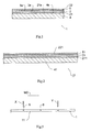
- Fig. 3 illustrates a conceptual view showing a series of steps of forming a partial removal portion on a solar battery element and cutting the solar battery element, and cutting out a solar battery cell from the element.
- the solar battery element 11 drawn out from a roll is carried in a longer direction MD.
- a partial removal portion 6 is formed by partially removing layers of the second electrode layer through to the light absorbing layer or the second electrode layer through to the first electrode layer using a machining tool X in the course of the carrying.
- the solar battery element 11 is cut at a partial removal portion forming region using a cutting tool Y, thereby obtaining a solar battery cell 1.
- one partial removal portion may be formed including the cutting schedule line, or at least two (a plurality of) partial removal portions may be formed in the vicinity of the cutting schedule line.
- the cutting schedule line is a designed position which is designed to cut out individual solar battery cells from the solar battery element.
- Fig. 4 illustrates a plan view of the solar battery element after a partial removal step is carried out.
- Fig. 5 illustrates a sectional view taken along the line V-V' in Fig. 4 , and illustrates a sectional view when layers of the second electrode layer through to the first electrode layer are partially removed.
- the solar battery element is described simply as an "element" in some cases.
- At least one partial removal portion 61 is formed at a part in the surface of the elongated solar battery element 11 by partially removing layers of the second electrode layer 221 through to the light absorbing layer 31 ( Figs. 4 and 5 ).
- the partial removal portion 61 extends like a belt when viewing the element 11 in a plane as in Fig. 4 , and is concave-shaped when viewing the element 11 in a cross section as in Fig. 5 . That is, the partial removal portion 61 is a portion in which a concave formed in the element 11 extends like a belt and linearly in a shorter direction of the element 11.
- the partial removal portion 61 is formed from a first end surface 611 and a second end surface 612, which are an aggregate of the end surfaces of layers of the second electrode layer 221 through to the light absorbing layer 31, and an electrode exposure surface 613 which is sandwiched between the first end surface 611 and the second end surface 612 and at which one surface of the first electrode layer 211 is exposed.
- the partial removal portion 61 is formed so as to include a cutting schedule line A.
- the partial removal portion 61 is formed so as to extend in a shorter direction TD of the elongated solar battery element 11.
- the partial removal portion 61 may be formed substantially in parallel with the shorter direction TD, or may be formed obliquely to the shorter direction in conformity to the shape of an ultimate solar battery module.
- the partial removal portion may be formed only along the shorter direction.
- the partial removal portion is also formed along the longer direction for cutting the element between rows (the same applies hereinafter).
- the width W of the partial removal portion 61 is not particularly limited. However, when the width W is excessively small, the first end surface 611 or second end surface 612 may be caused to sag in a processing direction as a cutting tool scrapes the first end surface 611 or second end surface 612 when the cutting tool is applied to the partial removal portion 61 in a later-described cutting step. From such a point of view, the width W of the partial removal portion 61 is preferably equal to or larger than the width of the cutting tool. For example, when a laser beam is used as a machining tool, a laser beam having a small line width of 30 ⁇ m is available.
- the width W of the partial removal portion 61 is preferably 30 ⁇ m or more, more preferably more than 40 ⁇ m, and especially preferably 50 ⁇ m or more.
- the width W of the partial removal portion 61 is preferably 20 mm or less, and more preferably 10 mm or less.
- Examples of the method for partially removing layers of the second electrode layer 221 through to the light absorbing layer 31 include mechanical machining such as machining by a knife edge-shaped cutlery and machining by a rotary blade, or machining by irradiation of laser beams. By using these machining tools, the above-described partial removal portion can be formed.
- a partial removal portion 62 is formed, as shown in Fig. 6 , from a first end surface 621 and a second end surface 622, which are an aggregate of the end surfaces of layers of the second electrode layer 221 through to the first electrode layer 211, and a base material exposure surface 623 which is sandwiched between the first end surface 621 and the second end surface 622 and at which one surface of the base material 41 is exposed.
- the process for partially removing layers of the second electrode layer 221 through to the first electrode layer 211 is the same as the process for partially removing layers from the second electrode layer 221 through to the light absorbing layer 31 as described above except that the first electrode layer 211 is also removed. Therefore, detailed descriptions thereof are omitted, and similar symbols are used for denotation in Fig. 6 .
- Fig. 7 illustrates a plan view of the solar battery element after a partial removal step is carried out.
- Fig. 8 illustrates a sectional view taken along the line VIII-VIII' in Fig. 7 , and illustrates a sectional view when layers of the second electrode layer through to the base material are partially removed.
- At least two partial removal portions 71 and 72 are formed at a part in the surface of the elongated solar battery element 11 by partially removing layers of the second electrode layer 221 through to the light absorbing layer 31 ( Figs. 7 and 8 ).
- Two partial removal portions 71 and 72 each extend like a belt when viewing the element 11 in a plane as in Fig. 7 , and are each concave-shaped when viewing the element 11 in a cross section as in Fig. 8 . That is, two partial removal portions 71 and 72 are each a portion in which a concave formed at a part in the surface of the element 11 extends like a belt and linearly in a predetermined direction of the element 11.
- the first partial removal portion 71 is formed from a first end surface 711 and a second end surface 712, which are an aggregate of the end surfaces of layers of the second electrode layer 221 through to the light absorbing layer 31, and an electrode exposure surface 713 which is sandwiched between the first end surface 711 and the second end surface 712 and at which one surface of the first electrode layer 211 is exposed.
- the second partial removal portion 72 is formed from a first end surface 721 and a second end surface 722, which are an aggregate of the end surfaces of layers of the second electrode layer 221 through to the light absorbing layer 31, and an electrode exposure surface 723 which is sandwiched between the first end surface 721 and the second end surface 722 and at which one surface of the first electrode layer 211 is exposed.
- the first partial removal portion 71 and the second partial removal portion 72 are formed so as to sandwich the cutting schedule line A therebetween.
- the first partial removal portion 71 and the second partial removal portion 72 are formed so as to extend in the shorter direction TD of the elongated solar battery element 11.
- the first partial removal portion 71 and the second partial removal portion 72 may be formed substantially in parallel with the shorter direction TD, or may be formed obliquely to the shorter direction.
- the widths W1 and W2 of the first partial removal portion 71 and the second partial removal portion 72 are not particularly limited. Since the first partial removal portion 71 and the second partial removal portion 72 are formed for partially separating the light absorbing layer 31 from the second electrode layer 221, the widths W1 and W2 are preferably as small as possible when considering the yield of the solar battery cell. When the widths W1 and W2 are excessively large, the yield of the solar battery cell is reduced, and therefore the widths W1 and W2 of the first partial removal portion 71 and the second partial removal portion 72 are preferably 3 mm or less, and more preferably 1 mm or less.
- the formation interval W3 between the first partial removal portion 71 and the second partial removal portion 72 (the interval W3 between the first end surface 711 of the first partial removal portion 71 and the second end surface 722 of the second partial removal portion 72) is not particularly limited. However, when the width W3 is excessively small, the first end surface 711 or the second end surface 722 may be caused to sag in a processing direction as a cutting tool scrapes the first end surface 711 or the second end surface 722 when the cutting tool is applied between the first partial removal portion 71 and the second partial removal portion 72 in a later-described cutting step.
- the formation interval W3 between the first partial removal portion 71 and the second partial removal portion 72 is preferably equal to or larger than the width of the cutting tool.
- the formation interval W3 between the first partial removal portion 71 and the second partial removal portion 72 is preferably 1 mm or more, more preferably more than 2 mm, and especially preferably 3 mm or more.
- the width W3 is excessively large, the yield of the solar battery cell is reduced, and adjacent solar battery cells may be short-circuited when obtained solar battery cells are electrically connected to form a solar battery module.
- the formation interval W3 between the first partial removal portion 71 and the second partial removal portion 72 is preferably 20 mm or less, and more preferably 10 mm or less.
- Three or more partial removal portions may be formed at the machining portion (not illustrated).
- the method for partially removing layers of the second electrode layer 221 through to the light absorbing layer 31 (method for forming the partial removal portion) is the same as the method described in the above section ⁇ Case where one partial removal portion is formed>.
- the method for partially removing layers of the second electrode layer 221 through to the first electrode layer 211 is also the same as the method in the above section ⁇ Case where one partial removal portion is formed>.
- layers above the first electrode layer or the base material can be partially removed to separate the layers.
- the removal is performed by mechanical machining such as machining by a knife edge-shaped cutlery and machining by a rotary blade, or machining by irradiation of laser beams
- the end surfaces (first end surface and second end surface) of the layers are hard to sag in a processing direction. Therefore, occurrence of short circuit of the first electrode layer and the second electrode layer can be prevented.
- peeling of the layers can also be prevented in layers of the second electrode layer through to the light absorbing layer.
- the cutting step is a step of cutting a solar battery element along a cutting schedule line or the vicinity thereof in a partial removal portion forming region after the partial removal step.
- the element 11 is cut at the partial removal portion 61 using a cutting tool.
- the cutting tool may be applied from the opening side of the partial removal portion 61 (second electrode layer side of the element 11), or may be applied from a side opposite to the opening side of the partial removal portion 61 (base material side of the element 11). Two cutting tools may be used to apply one cutting tool from the opening side of the partial removal portion 61 and apply the other cutting tool from a side opposite to the opening side of the partial removal portion 61.
- the cutting tool Y is applied so as to be fitted into the partial removal portion 61 formed so as to include the cutting schedule line A.
- the element 11 can be cut by the cutting tool Y without causing the cutting tool Y to come into contact with the first end surface 611 and the second end surface 612 of the partial removal portion 61.
- the cutting tool Y is aligned along the cutting schedule line A.
- Symbol Z shown by the two-dot chain line in Fig. 5 denotes a cutter stand that receives the cutting tool Y (the same applies in Fig. 8 ).
- the element 11 and the cutter stand Z are separated from each other, but actually the element 11 is placed on the cutter stand Z.
- the solar battery cell 1 can be cut out from the element 11.
- the edge of the base material of the obtained solar battery cell may be left to protrude outward slightly from the cut surface, but this does not affect the characteristics of the solar battery cell.
- Examples of the cutting tool include a push-cut blade, a rotary blade and the like.
- a push-cut blade having a relatively small width (blade thickness) and a length larger than the length of the element in the shorter direction is used.
- the element can be cut in a thickness direction by one pressing.
- the cutting tool may be applied from the opening side of the partial removal portions 71 and 72 or may be applied from a side opposite to the opening side, or two cutting tools may be used to apply one cutting tool from the opening side and apply the other cutting tool from a side opposite to the opening side.
- a stacked portion 11a of the second electrode layer 221, the light absorbing layer 31, the first electrode layer 211, and the base material 41 partially remains between the first partial removal portion 71 and the second partial removal portion 72.
- One cutting tool Y is applied to the stacked portion 11a from the opening side of the first partial removal portion 71 and the second partial removal portion 72 (cutting tool is shown by a two-dot chain line in Fig. 8 ).
- the cutting tool Y so as not to come into contact with the first end surface 711 of the first partial removal portion 71 and the second end surface 722 of the second partial removal portion 72. This is intended to prevent the first end surface 711 of the first partial removal portion 71 and the second end surface 722 of the second partial removal portion 72 from sagging due to contact with the cutting tool Y.
- the element 11 can be cut by the cutting tool Y without causing the cutting tool Y to come into contact with the first end surface 711 of the first partial removal portion 71 and the second end surface 722 of the second partial removal portion 72.
- the central part of the cutting tool Y in the width direction is aligned along the cutting schedule line A.
- the solar battery cell 1 can be cut out from the element 11.
- the cutting tool and the cutting method are the same as the cutting tool and the cutting method described in the above section ⁇ case where one partial removal portion is formed>.
- the solar battery cell of the present invention is obtained from a solar battery element by passing through the above steps.
- the method for producing a solar battery cell according to the present invention may include other steps in addition to the steps described above.
- the time required for cutting out solar battery cells from the element is equal to the time required for removal in the partial removal step. Therefore, according to the production method of the present invention, individual solar battery cells can be efficiently cut out from the solar battery element in a relatively short time while short circuit is prevented.
- the solar battery cell of the present invention can be used as a component of a solar battery module.
- Fig. 9 illustrates a schematic side view of a solar battery module which has a plurality of solar battery cells and is constituted by electrically connecting the plurality of solar battery cells.
- a plurality of solar battery cells 1 obtained by the production method described above are arranged between protective films 91 and 92 as shown in Fig. 9 while adjacent solar battery cells 1 are electrically connected, and a sealing resin 93 is injected, whereby a solar battery module 100 can be formed.
- the method for connecting adjacent solar battery cells 1 is not particularly limited.
- a plurality of solar battery cells 1 may be electrically connected in series by sequentially superimposing, on one end 22c of the second electrode layer 22 of one solar battery cell 1, the other end 4c of the base material 4 of the adjacent solar battery cell 1.
- the solar battery cells 1 are arranged with the cut surfaces 1a of the solar battery cells 1 made to face in a direction substantially orthogonal to a direction B along which the solar battery cells 1 are arranged side by side.
- the connecting method is not limited thereto, and the solar battery cells 1 may be arranged with the cut surfaces 1a of the solar battery cells 1 made to face in the direction B along which the solar battery cells 1 are arranged side by side (not illustrated).
- the solar battery cells may be arranged at intervals, followed by electrically connecting adjacent solar battery cells with a conducting wire (not illustrated).
- a SUS (stainless steel plate) having a width of 20 mm, a length of 100 m and a thickness of 50 ⁇ m was used as a base material.
- the base material was mounted in a sputtering device, and the inside of the sputtering device was evacuated. The ultimate degree of vacuum at this time was 2.0 ⁇ 10 -4 Pa.
- an Ar gas was introduced so as to achieve a pressure of 0.1 Pa using a mass flow controller (MFC), and a Cr layer (barrier layer) having a thickness of 0.3 ⁇ m was formed on one surface of the base material from a Cr target under the condition of a sputtering rate of 30 nm ⁇ min/m using a magnetron sputtering-type sputtering film formation method.
- the sputtering rate is a sputtering rate per unit carrying speed when sputtering is performed while the base material is carried.
- the base material with the barrier layer was mounted in a sputtering device, and the inside of the sputtering device was evacuated.
- the ultimate degree of vacuum at this time was 2.0 ⁇ 10 -4 Pa.
- an Ar gas was introduced so as to achieve a pressure of 0.1 Pa using a mass flow controller (MFC), and a Mo layer (first electrode layer) having a thickness of 0.3 ⁇ m was formed on one surface of the barrier layer from a Mo target under the condition of a sputtering rate of 30 nm ⁇ min/m using a DC magnetron sputtering-type sputtering film formation method.
- MFC mass flow controller
- a cell containing Ga, a cell containing In, a cell containing Cu and a cell containing Se were sequentially arranged as vapor deposition sources in a chamber of a vacuum vapor deposition device.
- the base material was mounted in the chamber, the inside of the chamber was evacuated to a degree of vacuum of 1.0 ⁇ 10 -4 Pa, and the base material was heated to 550°C.
- the vapor deposition sources were heated to 1150°C for Cu, 800°C for In, 950°C for Ga and 150°C for Se to vaporize the elements at the same time, thereby forming on one surface of the first electrode layer a CIGS layer (light absorbing layer) formed of a chalcopyrite compound.
- the carrying speed of the base material was 0.1 m/min.
- the formed light absorbing layer had a thickness of 2 ⁇ m as measured using a scanning electron microscope.
- 0.001 mol/l of cadmium acetate (Cd(CH 3 COOH) 2 ), 0.005 mol/l of thiourea (NH 2 CSNH 2 ), 0.01 mol/l of ammonium acetate and 0.4 mol/l of ammonia were mixed at room temperature.
- the elongated base material provided with the light absorbing layer was immersed in a rolled state in the mixed solution, and heated from room temperature to 80°C for 15 minutes using a water bath heated at 80°C, thereby forming a CdS layer (first buffer layer) on one surface of the light absorbing layer (CBD method).
- the formed CdS film had a thickness of about 70 nm as measured using a method called ellipsometry.
- the base material was mounted in a sputtering device so as to form a film on one surface of the first buffer layer, and the inside of the sputtering device was evacuated.
- the ultimate degree of vacuum at this time was 2.0 ⁇ 10 -4 Pa.
- an Ar gas was introduced so as to achieve a pressure of 0.2 Pa using a mass flow controller (MFC), and a ZnO layer (second buffer layer) having a thickness of 100 nm was formed from a ZnO target under the condition of a sputtering rate of 10 nm ⁇ min/m using a RF magnetron sputtering-type sputtering film formation method.
- MFC mass flow controller
- the base material was mounted in a sputtering device (manufactured by ULVAC, Inc.) so as to form a film on one surface of the second buffer layer, and the inside of the device was evacuated.
- the ultimate degree of vacuum at this time was 2.0 ⁇ 10 -4 Pa.
- an Ar gas was introduced so as to achieve a pressure of 0.3 Pa using a mass flow controller (MFC), and an ITO layer (second electrode layer) having a thickness of 0.5 ⁇ m was formed from an ITO target (In 2 O 3 :90 [% by atomic number], SnO 2 :10 [% by atomic number]) under the condition of a sputtering rate of 50 nm ⁇ min/m using a DC magnetron sputtering-type sputtering film formation method.
- MFC mass flow controller
- One partial removal portion was formed along a cutting schedule line of the prepared elongated solar battery element.
- a disc-shaped rotary blade coated with an artificial diamond abrasive grain (manufactured by DISCO Corporation, trade name: Z05-SD5000-D1A-105 54 ⁇ 2A3 ⁇ 40 ⁇ 45N-L-S3) was provided as a machining tool, and the solar battery element was machined while the rotary blade was rotated, so that partial removal portions extending like a belt in a shorter direction were formed at intervals of 300 mm in a longer direction of the element.
- the width of each partial removal portion was 1 mm, and layers of the ITO layer (second electrode layer) through to the CIGS layer (light absorbing layer) were machined.
- a push-cut blade having a blade tip angle of 30 degrees and a blade width of 2 mm was provided as a cutting tool, and the push-cut blade was pressed against the center of the partial removal portion to cut the whole solar battery element in a thickness direction, thereby obtaining a solar battery cell having a width of 20 mm and a length of 300 mm.
- An elongated solar battery element was prepared in the same manner as in Example 1.
- a solar battery cell was obtained by forming a partial removal portion on the element and cutting the element in the same manner as in Example 1 except that layers of the ITO layer (second electrode layer) through to the Mo layer (first electrode layer) were machined when the partial removal portion was formed.
- An elongated solar battery element was prepared in the same manner as in Example 1.
- Two partial removal portions were formed with a cutting schedule line of the prepared elongated solar battery element sandwiched therebetween.
- a disc-shaped rotary blade coated with an artificial diamond abrasive grain was provided as a machining tool, and the solar battery element was machined while the rotary blade was rotated, so that first partial removal portions extending like a belt in a shorter direction were formed at intervals of 300 mm in a longer direction of the element.
- the width of each first partial removal portion was 1 mm, and layers of the ITO layer (second electrode layer) through to the CIGS layer (light absorbing layer) were machined.
- second partial removal portions parallel to the first partial removal portions were each formed at a distance of 10 mm from the first partial removal portion to one side in the longer direction using the rotary blade.
- the width of each second partial removal portion was 1 mm, and layers of the ITO layer (second electrode layer) through to the CIGS layer (light absorbing layer) were machined.
- a push-cut blade having a blade tip angle of 30 degrees and a blade width of 2 mm was provided as a cutting tool, and the push-cut blade was pressed against a center with a width of 10 mm, which was sandwiched between the first partial removal portion and the second partial removal portion, to cut the whole solar battery element in a thickness direction, thereby obtaining a solar battery cell having a width of 20 mm and a length of 300 mm.
- An elongated solar battery element was prepared in the same manner as in Example 1.
- a solar battery cell was obtained by forming first and second partial removal portions on the element and cutting the element between the portions in the same manner as in Example 3 except that layers of the ITO layer (second electrode layer) through to the Mo layer (first electrode layer) were machined when the first and second partial removal portions were formed.
- An elongated solar battery element was prepared in the same manner as in Example 1.
- a push-cut blade having a blade tip angle of 30 degrees and a blade width of 2 mm was provided as a cutting tool to cut the whole solar battery element at intervals of 300 mm in a thickness direction, thereby obtaining a solar battery cell having a width of 20 mm and a length of 300 mm.
- Short circuit of the solar battery cell was evaluated based on the characteristics of the solar battery device.
- Evaluation was performed by visual observation on whether or not the light absorbing layer was peeled in association with power generation.
- the solar battery cells of Examples 1 to 4 obtained by cutting the solar battery element by a push-cut blade after performing partial removal by machining were capable of suppressing short circuit of electrode layers or the second electrode layer and the conductive material, and did not cause peeling of the light absorbing layer.
- the solar battery cell of Comparative Example obtained by cutting the solar battery element by a push-cut blade without performing machining was short-circuited and caused peeling of the light absorbing layer in a large number of samples.
Landscapes
- Engineering & Computer Science (AREA)
- Life Sciences & Earth Sciences (AREA)
- Forests & Forestry (AREA)
- Mechanical Engineering (AREA)
- Photovoltaic Devices (AREA)
- Nonmetal Cutting Devices (AREA)
- Manufacturing & Machinery (AREA)
Applications Claiming Priority (2)
| Application Number | Priority Date | Filing Date | Title |
|---|---|---|---|
| JP2011226514A JP2013089659A (ja) | 2011-10-14 | 2011-10-14 | 太陽電池セルの製造方法、及び太陽電池モジュール |
| PCT/JP2012/071406 WO2013054600A1 (ja) | 2011-10-14 | 2012-08-24 | 太陽電池セルの製造方法、及び太陽電池モジュール |
Publications (1)
| Publication Number | Publication Date |
|---|---|
| EP2768028A1 true EP2768028A1 (de) | 2014-08-20 |
Family
ID=48081660
Family Applications (1)
| Application Number | Title | Priority Date | Filing Date |
|---|---|---|---|
| EP12840555.2A Withdrawn EP2768028A1 (de) | 2011-10-14 | 2012-08-24 | Herstellungsverfahren für solarzelle und solarzellenmodul |
Country Status (5)
| Country | Link |
|---|---|
| US (1) | US20140216519A1 (de) |
| EP (1) | EP2768028A1 (de) |
| JP (1) | JP2013089659A (de) |
| KR (1) | KR20140071327A (de) |
| WO (1) | WO2013054600A1 (de) |
Cited By (2)
| Publication number | Priority date | Publication date | Assignee | Title |
|---|---|---|---|---|
| WO2016020797A3 (en) * | 2014-08-07 | 2016-04-14 | Ecosolifer Ag. | Solar cell element and cell arrangement made from the elements |
| FR3088141A1 (fr) * | 2018-11-07 | 2020-05-08 | S'tile | Dispositif photovoltaique |
Families Citing this family (11)
| Publication number | Priority date | Publication date | Assignee | Title |
|---|---|---|---|---|
| CN105097985B (zh) * | 2014-05-14 | 2019-02-01 | 北京汉能创昱科技有限公司 | 一种柔性薄膜太阳能电池制作的设备及方法 |
| KR102054420B1 (ko) * | 2014-05-27 | 2020-01-22 | 선파워 코포레이션 | 슁글드 태양 전지 모듈 |
| CL2016003045A1 (es) * | 2014-05-27 | 2017-06-09 | Sunpower Corp | Modulo escalonado de celda solar |
| JP2016119401A (ja) * | 2014-12-22 | 2016-06-30 | 日東電工株式会社 | 光電変換素子およびそれを用いた光電変換装置 |
| CN104526759A (zh) * | 2014-12-26 | 2015-04-22 | 苏州幸福新能源科技有限责任公司 | 太阳能背板开口装置 |
| JP6084648B2 (ja) | 2015-03-24 | 2017-02-22 | 株式会社東芝 | 光電変換素子および光電変換素子の製造方法 |
| CN106842669B (zh) * | 2017-04-06 | 2019-10-08 | 信利半导体有限公司 | 一种柔性彩膜基板及其制造方法 |
| KR102379388B1 (ko) * | 2017-08-24 | 2022-03-28 | 엘지전자 주식회사 | 태양 전지 및 이를 포함하는 태양 전지 패널 |
| CN110273144A (zh) * | 2018-03-14 | 2019-09-24 | 北京铂阳顶荣光伏科技有限公司 | 化学水浴沉积方法和cigs光伏组件的制备方法 |
| CN109261541A (zh) * | 2018-09-06 | 2019-01-25 | 苏州菲丽丝智能科技有限公司 | 一种锂电池检测分类机及其检测分类方法 |
| CN113399730B (zh) * | 2021-06-18 | 2025-11-14 | 东方日升(常州)新能源有限公司 | 切刀机构以及电池片串焊设备 |
Family Cites Families (14)
| Publication number | Priority date | Publication date | Assignee | Title |
|---|---|---|---|---|
| JPS61187377A (ja) * | 1985-02-15 | 1986-08-21 | Teijin Ltd | 非晶質太陽電池の分割加工方法 |
| US4704369A (en) * | 1985-04-01 | 1987-11-03 | Energy Conversion Devices, Inc. | Method of severing a semiconductor device |
| US5133810A (en) * | 1990-04-27 | 1992-07-28 | Sanyo Electric Co., Ltd. | Flexible photovoltaic device and manufacturing method thereof |
| JP2951060B2 (ja) * | 1990-12-27 | 1999-09-20 | 三洋電機株式会社 | 光起電力装置の製造方法 |
| US5385848A (en) * | 1993-09-20 | 1995-01-31 | Iowa Thin Film Technologies, Inc | Method for fabricating an interconnected array of semiconductor devices |
| JPH08116078A (ja) | 1994-10-17 | 1996-05-07 | Fuji Electric Co Ltd | 薄膜太陽電池の製造方法 |
| JP3537196B2 (ja) | 1994-11-08 | 2004-06-14 | 松下電器産業株式会社 | 太陽電池モジュールの作製方法 |
| JP2001053301A (ja) * | 1999-08-12 | 2001-02-23 | Kanegafuchi Chem Ind Co Ltd | 光電変換装置の製造方法 |
| JP2003158279A (ja) * | 2001-09-04 | 2003-05-30 | Canon Inc | 光起電力素子、光起電力素子集合体及び光起電力素子の製造方法 |
| JP4109585B2 (ja) | 2003-07-29 | 2008-07-02 | 松下電器産業株式会社 | プラズマ処理方法 |
| US7122398B1 (en) * | 2004-03-25 | 2006-10-17 | Nanosolar, Inc. | Manufacturing of optoelectronic devices |
| WO2008091890A2 (en) * | 2007-01-22 | 2008-07-31 | Solopower, Inc. | Roll-to-roll integration of thin film solar modules |
| JP2009130193A (ja) * | 2007-11-26 | 2009-06-11 | Toyota Motor Corp | 太陽電池モジュール |
| JP5648276B2 (ja) * | 2009-10-30 | 2015-01-07 | 三菱化学株式会社 | 太陽電池及びその製造方法 |
-
2011
- 2011-10-14 JP JP2011226514A patent/JP2013089659A/ja active Pending
-
2012
- 2012-08-24 US US14/346,174 patent/US20140216519A1/en not_active Abandoned
- 2012-08-24 EP EP12840555.2A patent/EP2768028A1/de not_active Withdrawn
- 2012-08-24 WO PCT/JP2012/071406 patent/WO2013054600A1/ja not_active Ceased
- 2012-08-24 KR KR1020147003363A patent/KR20140071327A/ko not_active Withdrawn
Cited By (2)
| Publication number | Priority date | Publication date | Assignee | Title |
|---|---|---|---|---|
| WO2016020797A3 (en) * | 2014-08-07 | 2016-04-14 | Ecosolifer Ag. | Solar cell element and cell arrangement made from the elements |
| FR3088141A1 (fr) * | 2018-11-07 | 2020-05-08 | S'tile | Dispositif photovoltaique |
Also Published As
| Publication number | Publication date |
|---|---|
| US20140216519A1 (en) | 2014-08-07 |
| JP2013089659A (ja) | 2013-05-13 |
| WO2013054600A1 (ja) | 2013-04-18 |
| KR20140071327A (ko) | 2014-06-11 |
Similar Documents
| Publication | Publication Date | Title |
|---|---|---|
| US20140216519A1 (en) | Method for producing solar battery cell and solar battery module | |
| JP5492354B1 (ja) | 結晶シリコン太陽電池の製造方法、太陽電池モジュールの製造方法、結晶シリコン太陽電池並びに太陽電池モジュール | |
| KR101378053B1 (ko) | 절연성 금속 기판 및 반도체 장치 | |
| CN101326645A (zh) | 太阳能电池 | |
| KR101081294B1 (ko) | 태양전지 및 이의 제조방법 | |
| JP2010165879A (ja) | スクライブ加工装置、及びスクライブ加工方法 | |
| WO2011089880A1 (en) | Solar cell and solar cell manufacturing method | |
| WO2007086521A1 (ja) | 太陽電池およびその製造方法 | |
| KR20140056169A (ko) | 박막 광발전 소자 및 제조 방법 | |
| JP5667027B2 (ja) | 太陽電池サブモジュール及びその製造方法、電極付き基板 | |
| US20130233382A1 (en) | Photoelectric conversion device | |
| JP2013141702A (ja) | スクライブ方法 | |
| US20130118578A1 (en) | Substrate for electronic device, and photoelectric conversion device including the same | |
| TW201635571A (zh) | 光電轉換元件及使用其之光電轉換裝置 | |
| JP2010242116A (ja) | 成膜方法と成膜装置、マスク、パターン膜、光電変換素子、及び太陽電池 | |
| KR101189432B1 (ko) | 태양전지 및 이의 제조방법 | |
| US9735307B2 (en) | Method of manufacturing thin-film solar cell | |
| JP4782855B2 (ja) | 化合物系薄膜太陽電池、及びその製造方法 | |
| US20130306146A1 (en) | Solar cell and method of manufacturing the same | |
| KR101034146B1 (ko) | 태양전지 및 이의 제조방법 | |
| JP5530618B2 (ja) | 光起電力素子、および、その製造方法 | |
| WO2013099947A1 (ja) | 光電変換装置 | |
| JP2005123391A (ja) | 太陽電池及びその製造方法 | |
| JP5997021B2 (ja) | 光電変換装置およびその製造方法 | |
| JP7070946B2 (ja) | 薄膜太陽電池用層構造を製造するための方法 |
Legal Events
| Date | Code | Title | Description |
|---|---|---|---|
| PUAI | Public reference made under article 153(3) epc to a published international application that has entered the european phase |
Free format text: ORIGINAL CODE: 0009012 |
|
| 17P | Request for examination filed |
Effective date: 20140319 |
|
| AK | Designated contracting states |
Kind code of ref document: A1 Designated state(s): AL AT BE BG CH CY CZ DE DK EE ES FI FR GB GR HR HU IE IS IT LI LT LU LV MC MK MT NL NO PL PT RO RS SE SI SK SM TR |
|
| DAX | Request for extension of the european patent (deleted) | ||
| STAA | Information on the status of an ep patent application or granted ep patent |
Free format text: STATUS: THE APPLICATION IS DEEMED TO BE WITHDRAWN |
|
| 18D | Application deemed to be withdrawn |
Effective date: 20150303 |