EP2768038A2 - Flexible Anzeigevorrichtung - Google Patents
Flexible Anzeigevorrichtung Download PDFInfo
- Publication number
- EP2768038A2 EP2768038A2 EP13183536.5A EP13183536A EP2768038A2 EP 2768038 A2 EP2768038 A2 EP 2768038A2 EP 13183536 A EP13183536 A EP 13183536A EP 2768038 A2 EP2768038 A2 EP 2768038A2
- Authority
- EP
- European Patent Office
- Prior art keywords
- display device
- flexible display
- actuator
- electrode
- display body
- Prior art date
- Legal status (The legal status is an assumption and is not a legal conclusion. Google has not performed a legal analysis and makes no representation as to the accuracy of the status listed.)
- Withdrawn
Links
Images


Classifications
-
- G—PHYSICS
- G09—EDUCATION; CRYPTOGRAPHY; DISPLAY; ADVERTISING; SEALS
- G09F—DISPLAYING; ADVERTISING; SIGNS; LABELS OR NAME-PLATES; SEALS
- G09F9/00—Indicating arrangements for variable information in which the information is built-up on a support by selection or combination of individual elements
-
- G—PHYSICS
- G02—OPTICS
- G02F—OPTICAL DEVICES OR ARRANGEMENTS FOR THE CONTROL OF LIGHT BY MODIFICATION OF THE OPTICAL PROPERTIES OF THE MEDIA OF THE ELEMENTS INVOLVED THEREIN; NON-LINEAR OPTICS; FREQUENCY-CHANGING OF LIGHT; OPTICAL LOGIC ELEMENTS; OPTICAL ANALOGUE/DIGITAL CONVERTERS
- G02F1/00—Devices or arrangements for the control of the intensity, colour, phase, polarisation or direction of light arriving from an independent light source, e.g. switching, gating or modulating; Non-linear optics
- G02F1/01—Devices or arrangements for the control of the intensity, colour, phase, polarisation or direction of light arriving from an independent light source, e.g. switching, gating or modulating; Non-linear optics for the control of the intensity, phase, polarisation or colour
- G02F1/03—Devices or arrangements for the control of the intensity, colour, phase, polarisation or direction of light arriving from an independent light source, e.g. switching, gating or modulating; Non-linear optics for the control of the intensity, phase, polarisation or colour based on ceramics or electro-optical crystals, e.g. exhibiting Pockels effect or Kerr effect
-
- G—PHYSICS
- G06—COMPUTING OR CALCULATING; COUNTING
- G06F—ELECTRIC DIGITAL DATA PROCESSING
- G06F3/00—Input arrangements for transferring data to be processed into a form capable of being handled by the computer; Output arrangements for transferring data from processing unit to output unit, e.g. interface arrangements
- G06F3/01—Input arrangements or combined input and output arrangements for interaction between user and computer
- G06F3/03—Arrangements for converting the position or the displacement of a member into a coded form
- G06F3/041—Digitisers, e.g. for touch screens or touch pads, characterised by the transducing means
-
- G—PHYSICS
- G09—EDUCATION; CRYPTOGRAPHY; DISPLAY; ADVERTISING; SEALS
- G09G—ARRANGEMENTS OR CIRCUITS FOR CONTROL OF INDICATING DEVICES USING STATIC MEANS TO PRESENT VARIABLE INFORMATION
- G09G5/00—Control arrangements or circuits for visual indicators common to cathode-ray tube indicators and other visual indicators
-
- H—ELECTRICITY
- H10—SEMICONDUCTOR DEVICES; ELECTRIC SOLID-STATE DEVICES NOT OTHERWISE PROVIDED FOR
- H10K—ORGANIC ELECTRIC SOLID-STATE DEVICES
- H10K59/00—Integrated devices, or assemblies of multiple devices, comprising at least one organic light-emitting element covered by group H10K50/00
-
- H—ELECTRICITY
- H10—SEMICONDUCTOR DEVICES; ELECTRIC SOLID-STATE DEVICES NOT OTHERWISE PROVIDED FOR
- H10K—ORGANIC ELECTRIC SOLID-STATE DEVICES
- H10K59/00—Integrated devices, or assemblies of multiple devices, comprising at least one organic light-emitting element covered by group H10K50/00
- H10K59/10—OLED displays
- H10K59/12—Active-matrix OLED [AMOLED] displays
-
- G—PHYSICS
- G02—OPTICS
- G02F—OPTICAL DEVICES OR ARRANGEMENTS FOR THE CONTROL OF LIGHT BY MODIFICATION OF THE OPTICAL PROPERTIES OF THE MEDIA OF THE ELEMENTS INVOLVED THEREIN; NON-LINEAR OPTICS; FREQUENCY-CHANGING OF LIGHT; OPTICAL LOGIC ELEMENTS; OPTICAL ANALOGUE/DIGITAL CONVERTERS
- G02F1/00—Devices or arrangements for the control of the intensity, colour, phase, polarisation or direction of light arriving from an independent light source, e.g. switching, gating or modulating; Non-linear optics
- G02F1/0009—Materials therefor
- G02F1/0018—Electro-optical materials
-
- G—PHYSICS
- G06—COMPUTING OR CALCULATING; COUNTING
- G06F—ELECTRIC DIGITAL DATA PROCESSING
- G06F3/00—Input arrangements for transferring data to be processed into a form capable of being handled by the computer; Output arrangements for transferring data from processing unit to output unit, e.g. interface arrangements
- G06F3/01—Input arrangements or combined input and output arrangements for interaction between user and computer
- G06F3/016—Input arrangements with force or tactile feedback as computer generated output to the user
-
- G—PHYSICS
- G09—EDUCATION; CRYPTOGRAPHY; DISPLAY; ADVERTISING; SEALS
- G09G—ARRANGEMENTS OR CIRCUITS FOR CONTROL OF INDICATING DEVICES USING STATIC MEANS TO PRESENT VARIABLE INFORMATION
- G09G2380/00—Specific applications
- G09G2380/02—Flexible displays
-
- H—ELECTRICITY
- H10—SEMICONDUCTOR DEVICES; ELECTRIC SOLID-STATE DEVICES NOT OTHERWISE PROVIDED FOR
- H10K—ORGANIC ELECTRIC SOLID-STATE DEVICES
- H10K2102/00—Constructional details relating to the organic devices covered by this subclass
- H10K2102/10—Transparent electrodes, e.g. using graphene
- H10K2102/101—Transparent electrodes, e.g. using graphene comprising transparent conductive oxides [TCO]
- H10K2102/103—Transparent electrodes, e.g. using graphene comprising transparent conductive oxides [TCO] comprising indium oxides, e.g. ITO
-
- H—ELECTRICITY
- H10—SEMICONDUCTOR DEVICES; ELECTRIC SOLID-STATE DEVICES NOT OTHERWISE PROVIDED FOR
- H10K—ORGANIC ELECTRIC SOLID-STATE DEVICES
- H10K2102/00—Constructional details relating to the organic devices covered by this subclass
- H10K2102/301—Details of OLEDs
- H10K2102/311—Flexible OLED
-
- H—ELECTRICITY
- H10—SEMICONDUCTOR DEVICES; ELECTRIC SOLID-STATE DEVICES NOT OTHERWISE PROVIDED FOR
- H10K—ORGANIC ELECTRIC SOLID-STATE DEVICES
- H10K59/00—Integrated devices, or assemblies of multiple devices, comprising at least one organic light-emitting element covered by group H10K50/00
- H10K59/10—OLED displays
-
- H—ELECTRICITY
- H10—SEMICONDUCTOR DEVICES; ELECTRIC SOLID-STATE DEVICES NOT OTHERWISE PROVIDED FOR
- H10K—ORGANIC ELECTRIC SOLID-STATE DEVICES
- H10K77/00—Constructional details of devices covered by this subclass and not covered by groups H10K10/80, H10K30/80, H10K50/80 or H10K59/80
- H10K77/10—Substrates, e.g. flexible substrates
- H10K77/111—Flexible substrates
Definitions
- the present invention relates to a flexible display device, and more particularly, to a flexible display device that is improved to control a physical change of the flexible display device.
- a flexible display device indicates a device that has flexibility by having a display unit formed on a flexible substrate such as polyimide.
- the flexible display device is very convenient since a shape of the flexible display device can be changed to reduce its size for portability.
- the present invention provides a flexible display device that is improved to exactly control a change state of the flexible display device and to decrease power consumption for changing and driving the flexible display device.
- a flexible display device including a display body having flexibility; an actuator for changing and driving the display body; and an initial shape forming substrate for maintaining an initial state of the display body before the display body is changed and driven.
- the actuator may include a first electrode and a second electrode which face each other, and an electro-active polymer layer that is interposed between the first electrode and the second electrode.
- the electro-active polymer layer When a voltage is applied to the first electrode and the second electrode, the electro-active polymer layer may extend whereby the flexible display device may be changed.
- the electro-active polymer layer may include polyvinylidene fluoride (PVDF), polydimethyl siloxane (PDMS), or polyvinylidene fluoride-co-trifluoroethylene (PVFT).
- PVDF polyvinylidene fluoride
- PDMS polydimethyl siloxane
- PVFT polyvinylidene fluoride-co-trifluoroethylene
- the first electrode and the second electrode may include an indium tin oxide (ITO) material.
- ITO indium tin oxide
- the actuator may be formed of one basic unit in which the electro-active polymer layer is interposed between the first electrode and the second electrode.
- the actuator may have a structure in which a plurality of basic units are stacked, wherein the electro-active polymer layer is interposed between the first electrode and the second electrode in each of the plurality of basic units.
- the initial shape forming substrate may maintain the initial state of the display body as a folding state, and when the actuator is driven, the display body may be turned into a flat state.
- the initial shape forming substrate may be formed of an alloy material including at least one of magnesium, aluminum, and lead.
- the display body may be attached to one surface of the initial shape forming substrate, and the actuator may be attached to another surface of the initial shape forming substrate.
- the display body may be attached to one surface of the actuator, and the initial shape forming substrate may be attached to another surface of the actuator.
- FIG. 1 illustrates a flexible display device 100 according to an embodiment of the present invention.
- the flexible display device 100 includes a display body 130 having flexibility, an initial shape forming substrate 120 that is attached on one surface of the display body 130, and an actuator 110 that is attached on another surface of the initial shape forming substrate 120.
- a reference numeral 101 indicates an adhesive layer.
- the display body 130 indicates a structure which includes a thin-film transistor (TFT) and a light-emitting device to realize an image, and an encapsulation layer to cover and protect the TFT and the light-emitting device that are stacked on a flexible substrate.
- TFT thin-film transistor
- encapsulation layer to cover and protect the TFT and the light-emitting device that are stacked on a flexible substrate.
- the structure is simply referred to as the display body 130. Since the display body 130 uses the flexible substrate, instead of a solid glass substrate, the display body 130 may be freely bent to the extent of the maximal flexibility of the display body 130.
- the initial shape forming substrate 120 is formed by casting an alloy of magnesium, aluminum, lead, or the like having a low elasticity modulus in a die, and functions to maintain an initial state of the flexible display device 100 as a folded state as shown in FIG. 2 . That is, the initial shape forming substrate 120 is formed to the folded state of a U-shape via the casting, and maintains the folding state unless an external force is applied in an opposite direction. Thus, the display body 130 that is combined with the initial shape forming substrate 120 maintains a folded state when it is not used. In other words, the default shape of the display is a folded state.
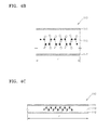
- the actuator 110 is attached to the initial shape forming substrate 120 through the adhesive layer 101 arranged between them, and has a structure in which an electro-active polymer layer 113 is interposed between first and second electrodes 111 and 112 that face each other as shown in FIG. 4A .
- the actuator 110 is driven by a principle in which a bending force is exerted since the electro-active polymer layer 113 extends according to a voltage that is applied to the first and second electrodes 111 and 112.
- FIGS. 4B and 4C are diagrams related to the principles of driving the actuator 110.
- the electro-active polymer layer 113 maintains its initial thickness and length L1.
- the voltage is applied to the first and second electrodes 111 and 112, as illustrated in FIG. 4C .
- the length L2 of the electro-active polymer layer 113 extends.
- the length L2 shown in FIG. 4C is greater than the length L1 shown in FIG. 4B .
- the surface of the actuator 110 is attached to and thus is restrained by the initial shape forming substrate 120, the other surface of the actuator 110 further extends, so that a bending force is exerted.
- the electro-active polymer layer 113 returns to the state of FIG. 4B before the bending force is exerted.
- the initial state by the initial shape forming substrate 120 is the U-shape folding state
- a state before the application of the voltage as shown in FIG. 4B is the folded state
- a state after the application of the voltage as shown in FIG. 4C is a flat state (or unfolded state).
- FIG. 3 illustrates a driving state in which the bending force of the actuator 110 is exerted.
- the flexible display device 100 maintains its U-shape folded state by the initial shape forming substrate 120, when the actuator 110 is driven, the bending force is exerted so that the flexible display device 100 is unfolded into the flat state.
- the flexible display device 100 Due to the bending force, when the actuator 110 is driven, the display body 130 that is combined with the actuator 110 is also unfolded. On the other hand, when the voltage applied to the actuator 110 is removed, the flexible display device 100 returns to the U-shape folding state that is initially set by the initial shape forming substrate 120.
- the electro-active polymer layer 113 may be formed of a material including polyvinylidene fluoride (PVDF), polydimethyl siloxane (PDMS), or polyvinylidene fluoride-co-trifluoroethylene (PVFT), and the first and second electrodes 111 and 112 may be formed of an indium tin oxide (ITO) material having flexibility.
- PVDF polyvinylidene fluoride
- PDMS polydimethyl siloxane
- PVFT polyvinylidene fluoride-co-trifluoroethylene
- ITO indium tin oxide
- the flexible display device 100 may be used as follows:
- the flexible display device 100 maintains its folded state by the initial shape forming substrate 120 as shown in FIG. 2 .
- a voltage is not applied to the actuator 110, no power is used, and thus the flexible display device 100 is carried or is placed. Since a length of the flexible display device 100 in the folding state is decreased by half, it is very convenient to carry and place the flexible display device 100.
- the voltage is not applied to the actuator 110 (referring to FIG. 4B ), useless power consumption does not occur while the flexible display device 100 is carried or is placed.
- the voltage is applied to the first and second electrodes 111 and 112 of the actuator 110. Then, the electro-active polymer layer 113 extends (referring to FIG. 4C ), so that the flexible display device 100 is unfolded (referring to FIG. 3 ) and then is finally turned into a flat state (referring to FIG. 1 .).
- the display body 130 at the flat state is driven, a user may watch images on a flat screen of the display body 130.
- the voltage that is applied to the actuator 110 is removed, so that the flexible display device 100 returns to the folding state that is set by the initial shape forming substrate 120.
- the folding state and the flat state are controlled by driving the actuator 110, it is very exact and convenient to fold and carry the flexible display device 100 and then to flatly unfold the flexible display device 100 for use.
- both portability and user convenience may be improved.
- the actuator 110 has a structure in which the electro-active polymer layer 113 is interposed between the first and second electrodes 111 and 112.
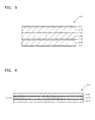
- an actuator 210 may have a multi-layer structure in which electro-active polymer layers 212, 214, and 216 are interposed between electrodes 211, 213, 215, and 217, respectively, i.e., a plurality of units are stacked while forming multiple layers.
- a bending force may be increased.
- the flexible display device 100 has the structure in which the display body 130 is attached to the surface of the initial shape forming substrate 120, and the actuator 110 is attached to the other surface of the initial shape forming substrate 120.
- a flexible display device 300 may have a structure in which a display body 330 is attached to a surface of an actuator 320, and an initial shape forming substrate 310 is attached to a surface of the actuator 320.
- a bending force may be decreased.
- an appropriate bending force may be achieved.
- the flexible display device when a user carries a flexible display device according to an embodiment of the present invention, the flexible display device maintains a folded state without power consumption, and then when the user uses the flexible display device, the flexible display device drives an actuator so that the user may unfold the flexible display device and may watch a flat screen. Accordingly, the flexible display device may be used with minimum power consumption, improved portability, and improved user convenience.
- the display shape can be changed between a first shape and a second shape by driving an actuator which is attached to the display.
- the first shape may be a folded shape which is adopted when the actuator is not driven.
- the second shape may be a flat shape which is adopted when the actuator is driven.
- the flexible display device allows a user to exactly control a change state of the flexible display device by driving the actuator and to decrease power consumption for changing and driving the flexible display device.
- the flexible display device allows a user to exactly control a change state of the flexible display device by driving the actuator and to decrease power consumption for changing and driving the flexible display device.
Landscapes
- Engineering & Computer Science (AREA)
- Physics & Mathematics (AREA)
- General Physics & Mathematics (AREA)
- Theoretical Computer Science (AREA)
- Nonlinear Science (AREA)
- General Engineering & Computer Science (AREA)
- Crystallography & Structural Chemistry (AREA)
- Chemical & Material Sciences (AREA)
- Ceramic Engineering (AREA)
- Optics & Photonics (AREA)
- Computer Hardware Design (AREA)
- Devices For Indicating Variable Information By Combining Individual Elements (AREA)
- Human Computer Interaction (AREA)
- Microelectronics & Electronic Packaging (AREA)
- Electroluminescent Light Sources (AREA)
Applications Claiming Priority (1)
| Application Number | Priority Date | Filing Date | Title |
|---|---|---|---|
| KR1020130015532A KR102048922B1 (ko) | 2013-02-13 | 2013-02-13 | 플렉시블 디스플레이 장치 |
Publications (2)
| Publication Number | Publication Date |
|---|---|
| EP2768038A2 true EP2768038A2 (de) | 2014-08-20 |
| EP2768038A3 EP2768038A3 (de) | 2017-12-06 |
Family
ID=49118396
Family Applications (1)
| Application Number | Title | Priority Date | Filing Date |
|---|---|---|---|
| EP13183536.5A Withdrawn EP2768038A3 (de) | 2013-02-13 | 2013-09-09 | Flexible Anzeigevorrichtung |
Country Status (5)
| Country | Link |
|---|---|
| US (1) | US9053651B2 (de) |
| EP (1) | EP2768038A3 (de) |
| JP (1) | JP6310706B2 (de) |
| KR (1) | KR102048922B1 (de) |
| CN (1) | CN103985338B (de) |
Cited By (1)
| Publication number | Priority date | Publication date | Assignee | Title |
|---|---|---|---|---|
| DE102014113732A1 (de) * | 2014-09-23 | 2016-03-24 | Osram Oled Gmbh | Optoelektronische Baugruppe und Verfahren zum Herstellen einer optoelektronischen Baugruppe |
Families Citing this family (33)
| Publication number | Priority date | Publication date | Assignee | Title |
|---|---|---|---|---|
| KR101940187B1 (ko) * | 2012-10-25 | 2019-01-21 | 삼성디스플레이 주식회사 | 양면 표시 장치 및 그 제조 방법 |
| KR101404628B1 (ko) * | 2013-05-29 | 2014-06-11 | 김선종 | 휘어짐이 가능한 전자기기 |
| KR102034002B1 (ko) * | 2014-08-26 | 2019-10-21 | 한국전자통신연구원 | 디스플레이 장치 및 그 제조 방법 |
| KR102226694B1 (ko) * | 2014-09-01 | 2021-03-11 | 엘지디스플레이 주식회사 | 접이식 디스플레이 장치 |
| KR102228857B1 (ko) * | 2014-09-05 | 2021-03-17 | 엘지전자 주식회사 | 휴대 전자기기 |
| KR102322762B1 (ko) | 2014-09-15 | 2021-11-08 | 삼성디스플레이 주식회사 | 디스플레이 장치 |
| KR102319835B1 (ko) * | 2014-09-22 | 2021-11-01 | 엘지디스플레이 주식회사 | 접이식 디스플레이 장치 |
| CN104469632B (zh) * | 2014-11-28 | 2018-02-02 | 华勤通讯技术有限公司 | 一种发声方法及发声装置 |
| US20160179230A1 (en) * | 2014-12-23 | 2016-06-23 | Intel Corporation | Electroactive layer coupled to a flexible display |
| EP3041058B1 (de) * | 2014-12-31 | 2019-09-11 | LG Display Co., Ltd. | Mehrschichtige umwandelbare vorrichtung und anzeigevorrichtung damit |
| US10042394B2 (en) | 2014-12-31 | 2018-08-07 | Lg Display Co., Ltd. | Foldable plate and foldable display device with the same |
| KR20160089164A (ko) * | 2015-01-19 | 2016-07-27 | 삼성전자주식회사 | 플렉서블 디바이스의 디스플레이의 형상을 제어하는 방법 및 플렉서블 디바이스 |
| CN104536162B (zh) * | 2015-01-19 | 2018-08-21 | 昆山国显光电有限公司 | 透明显示控制结构及透明显示装置 |
| CN104536187B (zh) * | 2015-01-23 | 2018-01-23 | 京东方科技集团股份有限公司 | 柔性显示器 |
| CN104658430A (zh) * | 2015-02-28 | 2015-05-27 | 北京维信诺科技有限公司 | 一种柔性显示装置 |
| KR102387038B1 (ko) | 2015-05-19 | 2022-04-15 | 삼성디스플레이 주식회사 | 표시 장치 |
| US10061357B2 (en) * | 2015-06-10 | 2018-08-28 | Intel Corporation | Electroactive layer to coil a flexible display |
| KR102378758B1 (ko) * | 2015-06-19 | 2022-03-25 | 엘지디스플레이 주식회사 | 플렉서블 표시 장치 |
| US10345905B2 (en) * | 2015-09-08 | 2019-07-09 | Apple Inc. | Electronic devices with deformable displays |
| CN106873814B (zh) * | 2015-12-14 | 2020-02-21 | 联想(北京)有限公司 | 一种控制方法及电子设备 |
| KR102490890B1 (ko) | 2016-01-11 | 2023-01-25 | 삼성디스플레이 주식회사 | 디스플레이 장치 |
| KR20170088565A (ko) * | 2016-01-25 | 2017-08-02 | 삼성전자주식회사 | 휴대용 전자 장치의 보호용 케이스 및 케이스의 상태 판단 방법 |
| CN105508889A (zh) * | 2016-02-01 | 2016-04-20 | 京东方科技集团股份有限公司 | 发光组件及其制作方法 |
| JP6851362B2 (ja) * | 2016-02-18 | 2021-03-31 | ダウ・東レ株式会社 | フレキシブル積層体及びそれを用いたフレキシブルディスプレイ |
| JP6271828B1 (ja) * | 2016-04-26 | 2018-01-31 | 東レ・ダウコーニング株式会社 | フレキシブル積層体及びそれを備えたフレキシブルディスプレイ |
| CN106601132B (zh) * | 2017-01-04 | 2019-12-03 | 昆山国显光电有限公司 | 一种柔性显示装置及其控制方法 |
| US10539993B2 (en) * | 2017-03-14 | 2020-01-21 | Microsoft Technology Licensing, Llc | Integrated energy storage systems in computing facilities |
| CN107240600B (zh) * | 2017-06-26 | 2019-10-18 | 京东方科技集团股份有限公司 | 一种柔性显示装置 |
| JP7077001B2 (ja) * | 2017-12-15 | 2022-05-30 | 株式会社ジャパンディスプレイ | 表示装置 |
| KR102483893B1 (ko) * | 2018-02-09 | 2023-01-02 | 삼성디스플레이 주식회사 | 플렉서블 표시 장치 |
| KR102827056B1 (ko) * | 2019-04-16 | 2025-07-01 | 엘지이노텍 주식회사 | 플렉서블 회로기판 및 이를 포함하는 플렉서블 장치 |
| US11810487B2 (en) | 2020-11-30 | 2023-11-07 | Rovi Guides, Inc. | Display system for directing different images to different viewers |
| NL2028249B1 (en) * | 2021-05-19 | 2022-12-06 | Microsoft Technology Licensing Llc | Active slack management in a layered article |
Family Cites Families (25)
| Publication number | Priority date | Publication date | Assignee | Title |
|---|---|---|---|---|
| US4266339A (en) * | 1979-06-07 | 1981-05-12 | Dielectric Systems International, Inc. | Method for making rolling electrode for electrostatic device |
| JP2003280546A (ja) * | 2002-03-27 | 2003-10-02 | Matsushita Electric Ind Co Ltd | 自己変形型フレキシブルディスプレイ及びそれを用いた情報処理端末 |
| US7456823B2 (en) * | 2002-06-14 | 2008-11-25 | Sony Corporation | User interface apparatus and portable information apparatus |
| TW200413776A (en) * | 2002-11-05 | 2004-08-01 | Matsushita Electric Industrial Co Ltd | Display element and display using the same |
| WO2004049050A1 (en) * | 2002-11-22 | 2004-06-10 | Koninklijke Philips Electronics N.V. | Method of manufacturing a curved display |
| US20050269943A1 (en) * | 2004-06-04 | 2005-12-08 | Michael Hack | Protected organic electronic devices and methods for making the same |
| US7714801B2 (en) * | 2005-01-05 | 2010-05-11 | Nokia Corporation | Foldable electronic device and a flexible display device |
| JP4732798B2 (ja) * | 2005-05-19 | 2011-07-27 | 株式会社日立製作所 | アクチュエーターおよびアクチュエーターモジュール |
| JP4732876B2 (ja) * | 2005-11-30 | 2011-07-27 | 株式会社日立製作所 | アクチュエータ、アクチュエータモジュールおよびアクチュエータモジュール製造方法 |
| JP2008151818A (ja) * | 2006-12-14 | 2008-07-03 | Hitachi Ltd | 表示装置 |
| US9823833B2 (en) * | 2007-06-05 | 2017-11-21 | Immersion Corporation | Method and apparatus for haptic enabled flexible touch sensitive surface |
| JPWO2009050812A1 (ja) * | 2007-10-18 | 2011-02-24 | 富士通株式会社 | 表示装置および表示システム |
| JP5258436B2 (ja) * | 2008-07-30 | 2013-08-07 | 株式会社東芝 | 表示装置及びその製造方法 |
| KR20100031027A (ko) | 2008-09-11 | 2010-03-19 | 전남대학교산학협력단 | 자기 치유 기능을 갖는 기전 고분자 작동기 및 그 작동기를포함하는 인공신체조직 |
| KR101067661B1 (ko) * | 2009-04-14 | 2011-09-27 | 한국과학기술원 | 이온에 의해 작동되는 전기 활성 폴리머를 이용한 유연 디스플레이 형상변형장치 및 그 방법 |
| WO2011016265A1 (ja) * | 2009-08-07 | 2011-02-10 | シャープ株式会社 | 表示素子、及び電気機器 |
| US20110084898A1 (en) * | 2009-10-14 | 2011-04-14 | Sony Corporation | Memory shape element for flexible oled display screen |
| WO2011105837A2 (ko) | 2010-02-24 | 2011-09-01 | (주) 씨아이제이 | 연성 전극소재 및 그 제조방법 |
| KR101809191B1 (ko) * | 2010-10-11 | 2018-01-18 | 삼성전자주식회사 | 터치 패널 |
| JP5299406B2 (ja) | 2010-11-10 | 2013-09-25 | コニカミノルタ株式会社 | 平面状表示装置、表示制御方法および表示制御プログラム |
| EP3364636B1 (de) * | 2011-03-21 | 2021-02-10 | Apple Inc. | Elektronische vorrichtung mit flexiblen anzeigen |
| KR101245375B1 (ko) * | 2011-06-08 | 2013-03-20 | 주식회사 팬택 | 능동적 플렉서블 디스플레이, 능동적 플렉서블 디스플레이의 제어 장치 및 방법 |
| KR101340716B1 (ko) * | 2011-08-25 | 2013-12-12 | 주식회사 팬택 | 플렉서블 디스플레이 제어 장치 및 제어 방법 |
| CN102629015A (zh) * | 2012-03-27 | 2012-08-08 | 京东方科技集团股份有限公司 | 柔性显示装置及其制作方法 |
| KR101661526B1 (ko) * | 2012-04-08 | 2016-10-04 | 삼성전자주식회사 | 플렉서블 디스플레이 장치 및 그 ui 방법 |
-
2013
- 2013-02-13 KR KR1020130015532A patent/KR102048922B1/ko active Active
- 2013-06-26 US US13/927,318 patent/US9053651B2/en active Active
- 2013-08-29 CN CN201310384460.4A patent/CN103985338B/zh active Active
- 2013-09-09 EP EP13183536.5A patent/EP2768038A3/de not_active Withdrawn
-
2014
- 2014-01-23 JP JP2014010320A patent/JP6310706B2/ja active Active
Non-Patent Citations (1)
| Title |
|---|
| None |
Cited By (3)
| Publication number | Priority date | Publication date | Assignee | Title |
|---|---|---|---|---|
| DE102014113732A1 (de) * | 2014-09-23 | 2016-03-24 | Osram Oled Gmbh | Optoelektronische Baugruppe und Verfahren zum Herstellen einer optoelektronischen Baugruppe |
| US10082270B2 (en) | 2014-09-23 | 2018-09-25 | Osram Oled Gmbh | Optoelectronic module and method for producing an optoelectronic module |
| DE102014113732B4 (de) | 2014-09-23 | 2022-11-24 | Pictiva Displays International Limited | 3D-OLED und Verfahren zum Herstellen einer 3D-OLED |
Also Published As
| Publication number | Publication date |
|---|---|
| KR102048922B1 (ko) | 2020-01-09 |
| CN103985338A (zh) | 2014-08-13 |
| US9053651B2 (en) | 2015-06-09 |
| KR20140102087A (ko) | 2014-08-21 |
| JP2014153711A (ja) | 2014-08-25 |
| US20130286462A1 (en) | 2013-10-31 |
| EP2768038A3 (de) | 2017-12-06 |
| JP6310706B2 (ja) | 2018-04-11 |
| CN103985338B (zh) | 2017-05-17 |
Similar Documents
| Publication | Publication Date | Title |
|---|---|---|
| EP2768038A2 (de) | Flexible Anzeigevorrichtung | |
| JP7119192B2 (ja) | 電子機器、及び、表示装置 | |
| CN114283693B (zh) | 柔性显示屏 | |
| CN115273705B (zh) | 显示设备 | |
| CN105742480B (zh) | 多层可变形装置和包含该多层可变形装置的显示装置 | |
| TWI690076B (zh) | 可撓顯示器最適安裝技術 | |
| US20130265631A1 (en) | Flexible display apparatus | |
| KR102573789B1 (ko) | 플렉서블 표시 장치 | |
| JP2011081069A (ja) | 表示装置 | |
| KR102114318B1 (ko) | 플렉시블 디스플레이 장치 | |
| TWI631740B (zh) | 多層可變形裝置及包含該多層可變形裝置的顯示裝置 | |
| JP5499967B2 (ja) | 表示機能付きicカード | |
| KR20210086027A (ko) | 표시장치 | |
| KR20160081760A (ko) | 다층 가변 소자 및 이를 포함하는 표시 장치 |
Legal Events
| Date | Code | Title | Description |
|---|---|---|---|
| PUAI | Public reference made under article 153(3) epc to a published international application that has entered the european phase |
Free format text: ORIGINAL CODE: 0009012 |
|
| 17P | Request for examination filed |
Effective date: 20130909 |
|
| AK | Designated contracting states |
Kind code of ref document: A2 Designated state(s): AL AT BE BG CH CY CZ DE DK EE ES FI FR GB GR HR HU IE IS IT LI LT LU LV MC MK MT NL NO PL PT RO RS SE SI SK SM TR |
|
| AX | Request for extension of the european patent |
Extension state: BA ME |
|
| RAP1 | Party data changed (applicant data changed or rights of an application transferred) |
Owner name: SAMSUNG DISPLAY CO., LTD. |
|
| PUAL | Search report despatched |
Free format text: ORIGINAL CODE: 0009013 |
|
| AK | Designated contracting states |
Kind code of ref document: A3 Designated state(s): AL AT BE BG CH CY CZ DE DK EE ES FI FR GB GR HR HU IE IS IT LI LT LU LV MC MK MT NL NO PL PT RO RS SE SI SK SM TR |
|
| AX | Request for extension of the european patent |
Extension state: BA ME |
|
| RIC1 | Information provided on ipc code assigned before grant |
Ipc: H01L 51/00 20060101AFI20171101BHEP Ipc: H01L 27/32 20060101ALI20171101BHEP |
|
| R17P | Request for examination filed (corrected) |
Effective date: 20180425 |
|
| RBV | Designated contracting states (corrected) |
Designated state(s): AL AT BE BG CH CY CZ DE DK EE ES FI FR GB GR HR HU IE IS IT LI LT LU LV MC MK MT NL NO PL PT RO RS SE SI SK SM TR |
|
| STAA | Information on the status of an ep patent application or granted ep patent |
Free format text: STATUS: EXAMINATION IS IN PROGRESS |
|
| 17Q | First examination report despatched |
Effective date: 20190401 |
|
| STAA | Information on the status of an ep patent application or granted ep patent |
Free format text: STATUS: THE APPLICATION IS DEEMED TO BE WITHDRAWN |
|
| 18D | Application deemed to be withdrawn |
Effective date: 20190813 |