EP2772765A1 - Nanoélectrode et procédé de fabrication de cette dernière - Google Patents
Nanoélectrode et procédé de fabrication de cette dernière Download PDFInfo
- Publication number
- EP2772765A1 EP2772765A1 EP20120844016 EP12844016A EP2772765A1 EP 2772765 A1 EP2772765 A1 EP 2772765A1 EP 20120844016 EP20120844016 EP 20120844016 EP 12844016 A EP12844016 A EP 12844016A EP 2772765 A1 EP2772765 A1 EP 2772765A1
- Authority
- EP
- European Patent Office
- Prior art keywords
- nano
- electrode
- nano wire
- probe
- insulation film
- Prior art date
- Legal status (The legal status is an assumption and is not a legal conclusion. Google has not performed a legal analysis and makes no representation as to the accuracy of the status listed.)
- Withdrawn
Links
- 238000004519 manufacturing process Methods 0.000 title claims description 8
- 239000002070 nanowire Substances 0.000 claims abstract description 50
- 239000000523 sample Substances 0.000 claims abstract description 37
- 238000009413 insulation Methods 0.000 claims abstract description 28
- 238000000034 method Methods 0.000 claims description 18
- PXHVJJICTQNCMI-UHFFFAOYSA-N Nickel Chemical compound [Ni] PXHVJJICTQNCMI-UHFFFAOYSA-N 0.000 claims description 12
- BASFCYQUMIYNBI-UHFFFAOYSA-N platinum Chemical compound [Pt] BASFCYQUMIYNBI-UHFFFAOYSA-N 0.000 claims description 12
- 238000007747 plating Methods 0.000 claims description 9
- 238000005520 cutting process Methods 0.000 claims description 8
- 229920001940 conductive polymer Polymers 0.000 claims description 7
- 229910052782 aluminium Inorganic materials 0.000 claims description 6
- XAGFODPZIPBFFR-UHFFFAOYSA-N aluminium Chemical compound [Al] XAGFODPZIPBFFR-UHFFFAOYSA-N 0.000 claims description 6
- PCHJSUWPFVWCPO-UHFFFAOYSA-N gold Chemical compound [Au] PCHJSUWPFVWCPO-UHFFFAOYSA-N 0.000 claims description 6
- 229910052737 gold Inorganic materials 0.000 claims description 6
- 239000010931 gold Substances 0.000 claims description 6
- 229910052759 nickel Inorganic materials 0.000 claims description 6
- 239000003973 paint Substances 0.000 claims description 6
- 229910052697 platinum Inorganic materials 0.000 claims description 6
- 229920000052 poly(p-xylylene) Polymers 0.000 claims description 6
- OKTJSMMVPCPJKN-UHFFFAOYSA-N Carbon Chemical compound [C] OKTJSMMVPCPJKN-UHFFFAOYSA-N 0.000 claims description 4
- 239000002041 carbon nanotube Substances 0.000 claims description 4
- 229910021393 carbon nanotube Inorganic materials 0.000 claims description 4
- 238000010884 ion-beam technique Methods 0.000 claims description 4
- 229920000767 polyaniline Polymers 0.000 claims description 4
- 229920000128 polypyrrole Polymers 0.000 claims description 4
- 238000004720 dielectrophoresis Methods 0.000 claims description 3
- WFKWXMTUELFFGS-UHFFFAOYSA-N tungsten Chemical compound [W] WFKWXMTUELFFGS-UHFFFAOYSA-N 0.000 claims description 3
- 229910052721 tungsten Inorganic materials 0.000 claims description 2
- 239000010937 tungsten Substances 0.000 claims description 2
- RYGMFSIKBFXOCR-UHFFFAOYSA-N Copper Chemical compound [Cu] RYGMFSIKBFXOCR-UHFFFAOYSA-N 0.000 claims 1
- 229910052802 copper Inorganic materials 0.000 claims 1
- 239000010949 copper Substances 0.000 claims 1
- 238000002484 cyclic voltammetry Methods 0.000 description 5
- 239000010410 layer Substances 0.000 description 5
- 238000003487 electrochemical reaction Methods 0.000 description 4
- 238000005530 etching Methods 0.000 description 4
- 239000012774 insulation material Substances 0.000 description 4
- 239000000203 mixture Substances 0.000 description 4
- 229910052581 Si3N4 Inorganic materials 0.000 description 3
- 229910052751 metal Inorganic materials 0.000 description 3
- 239000002184 metal Substances 0.000 description 3
- HQVNEWCFYHHQES-UHFFFAOYSA-N silicon nitride Chemical compound N12[Si]34N5[Si]62N3[Si]51N64 HQVNEWCFYHHQES-UHFFFAOYSA-N 0.000 description 3
- 238000006243 chemical reaction Methods 0.000 description 2
- 238000000151 deposition Methods 0.000 description 2
- 238000010191 image analysis Methods 0.000 description 2
- 239000007788 liquid Substances 0.000 description 2
- 238000006479 redox reaction Methods 0.000 description 2
- -1 region Substances 0.000 description 2
- 230000005641 tunneling Effects 0.000 description 2
- 229910020427 K2PtCl4 Inorganic materials 0.000 description 1
- VYPSYNLAJGMNEJ-UHFFFAOYSA-N Silicium dioxide Chemical compound O=[Si]=O VYPSYNLAJGMNEJ-UHFFFAOYSA-N 0.000 description 1
- 238000005229 chemical vapour deposition Methods 0.000 description 1
- 230000003247 decreasing effect Effects 0.000 description 1
- 230000007547 defect Effects 0.000 description 1
- 238000007598 dipping method Methods 0.000 description 1
- 230000000694 effects Effects 0.000 description 1
- 230000005684 electric field Effects 0.000 description 1
- 238000005516 engineering process Methods 0.000 description 1
- 239000000463 material Substances 0.000 description 1
- 238000005259 measurement Methods 0.000 description 1
- 238000012986 modification Methods 0.000 description 1
- 230000004048 modification Effects 0.000 description 1
- 239000002071 nanotube Substances 0.000 description 1
- 238000006722 reduction reaction Methods 0.000 description 1
- 229910052814 silicon oxide Inorganic materials 0.000 description 1
- 239000002356 single layer Substances 0.000 description 1
- 239000000758 substrate Substances 0.000 description 1
Images


Classifications
-
- H—ELECTRICITY
- H01—ELECTRIC ELEMENTS
- H01B—CABLES; CONDUCTORS; INSULATORS; SELECTION OF MATERIALS FOR THEIR CONDUCTIVE, INSULATING OR DIELECTRIC PROPERTIES
- H01B7/00—Insulated conductors or cables characterised by their form
-
- G—PHYSICS
- G01—MEASURING; TESTING
- G01Q—SCANNING-PROBE TECHNIQUES OR APPARATUS; APPLICATIONS OF SCANNING-PROBE TECHNIQUES, e.g. SCANNING PROBE MICROSCOPY [SPM]
- G01Q70/00—General aspects of SPM probes, their manufacture or their related instrumentation, insofar as they are not specially adapted to a single SPM technique covered by group G01Q60/00
- G01Q70/08—Probe characteristics
- G01Q70/10—Shape or taper
- G01Q70/12—Nanotube tips
-
- G—PHYSICS
- G01—MEASURING; TESTING
- G01Q—SCANNING-PROBE TECHNIQUES OR APPARATUS; APPLICATIONS OF SCANNING-PROBE TECHNIQUES, e.g. SCANNING PROBE MICROSCOPY [SPM]
- G01Q70/00—General aspects of SPM probes, their manufacture or their related instrumentation, insofar as they are not specially adapted to a single SPM technique covered by group G01Q60/00
- G01Q70/16—Probe manufacture
-
- G—PHYSICS
- G01—MEASURING; TESTING
- G01Q—SCANNING-PROBE TECHNIQUES OR APPARATUS; APPLICATIONS OF SCANNING-PROBE TECHNIQUES, e.g. SCANNING PROBE MICROSCOPY [SPM]
- G01Q60/00—Particular types of SPM [Scanning Probe Microscopy] or microscopes; Essential components thereof
- G01Q60/24—AFM [Atomic Force Microscopy] or apparatus therefor, e.g. AFM probes
-
- H—ELECTRICITY
- H01—ELECTRIC ELEMENTS
- H01B—CABLES; CONDUCTORS; INSULATORS; SELECTION OF MATERIALS FOR THEIR CONDUCTIVE, INSULATING OR DIELECTRIC PROPERTIES
- H01B13/00—Apparatus or processes specially adapted for manufacturing conductors or cables
- H01B13/06—Insulating conductors or cables
-
- B—PERFORMING OPERATIONS; TRANSPORTING
- B82—NANOTECHNOLOGY
- B82Y—SPECIFIC USES OR APPLICATIONS OF NANOSTRUCTURES; MEASUREMENT OR ANALYSIS OF NANOSTRUCTURES; MANUFACTURE OR TREATMENT OF NANOSTRUCTURES
- B82Y15/00—Nanotechnology for interacting, sensing or actuating, e.g. quantum dots as markers in protein assays or molecular motors
-
- B—PERFORMING OPERATIONS; TRANSPORTING
- B82—NANOTECHNOLOGY
- B82Y—SPECIFIC USES OR APPLICATIONS OF NANOSTRUCTURES; MEASUREMENT OR ANALYSIS OF NANOSTRUCTURES; MANUFACTURE OR TREATMENT OF NANOSTRUCTURES
- B82Y35/00—Methods or apparatus for measurement or analysis of nanostructures
-
- G—PHYSICS
- G01—MEASURING; TESTING
- G01Q—SCANNING-PROBE TECHNIQUES OR APPARATUS; APPLICATIONS OF SCANNING-PROBE TECHNIQUES, e.g. SCANNING PROBE MICROSCOPY [SPM]
- G01Q60/00—Particular types of SPM [Scanning Probe Microscopy] or microscopes; Essential components thereof
- G01Q60/60—SECM [Scanning Electro-Chemical Microscopy] or apparatus therefor, e.g. SECM probes
Definitions
- the present invention relates to a nano electrode, and particularly, to a probe-type nano electrode and a method of manufacturing the same.
- ATM atomic force microscope
- a pyramid-shaped sharp probe is formed at an end of a small rod that is called a cantilever, and an image resolution and reproducibility of the atomic force microscope are determined according to a shape and a size of the probe.
- An end of the probe may be sharpened by using a method such as etching, but it is not easy to control the size and the shape of the probe by using etching, and additionally, a material to which this method may be applied is limitative.
- the probe may be used in a functional atomic force microscope, the scanning tunneling microscope, or the like by analyzing an electrochemical reaction in a fine region.
- the present invention has been made in an effort to provide a nano electrode in which an electrode is manufactured at a level of several hundred nanometers to precisely measure an electrochemical reaction of a fine region, and a method of manufacturing the same.
- An exemplary embodiment of the present invention provides a nano electrode including: a main body having a protruding probe, a nano wire attached to the probe, and an insulation film surrounding the nano wire and including an opening through which an upper surface of the nano wire is exposed.
- the nano electrode may further include an electrode positioned on the upper surface of the nano wire, and the electrode may be formed of any one of gold, platinum, aluminum, or nickel.
- the insulation film may include at least one of parylene, an oxynitride film, and an electrophoretic paint.
- Another exemplary embodiment of the present invention provides a method of manufacturing a nano electrode, including: preparing a main body including a probe, attaching a nano wire to an end of the probe, forming an insulation film on the nano wire, and cutting the nano wire and the insulation film to expose a cross section of the nano wire and thus form a cross-sectional electrode.
- the method may further include forming an electrode on the cross section of the nano wire, and the electrode may be formed by plating.
- the plating may be formed by any one of gold, platinum, aluminum, or nickel.
- the insulation film may be formed by parylene, an oxynitride film, or an electrophoretic paint.
- the nano wire may be formed of a carbon nano tube or a conductive polymer.
- the conductive polymer may include polypyrrole or polyaniline.
- the cutting may be performed by a focused ion beam.
- the attaching of the nano wire may be performed by a dielectrophoresis method.
- a nano electrode is formed according to the present invention, since only an upper portion of a probe can be selectively used as an electrode, it is possible to precisely measure an electrochemical reaction of a fine region.
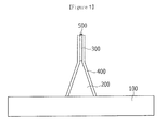
- FIG. 1 is a cross-sectional view schematically illustrating a shape of a nano probe according to an exemplary embodiment of the present invention.
- the nano electrode according to the present invention includes a main body 100, a probe 200 protruding from the main body 100, a nano wire 300 attached to an end of the probe 200, an insulation film 400 surrounding the nano wire 300, and a nano electrode 500 formed on an upper surface of the nano wire 300.
- the main body 100 is a portion to which the probe is attached, and may be a cantilever of an atomic force microscope.
- the probe 200 protrudes in a vertical direction to the main body 100, and may be a tungsten tip or a tip of the atomic force microscope having a pyramid shape where a width is decreased toward an end.
- the nano wire 300 may be formed of a carbon nano tube or a conductive polymer, and examples of the conductive polymer include polypyrrole and polyaniline.
- the nano wire has a rod shape, and an end of the nano wire is attached to the end of the probe to increase a length of the protruding probe and thus further sharpen the end of the probe.
- the nano wire 300 has a diameter of several tens nm to several hundreds nm.
- the insulation film 400 surrounds a side wall of the nano wire 300, and includes a cut portion through which the upper surface of the nano wire 300 is exposed.
- the insulation film 400 may be formed of an insulation material such as parylene, an electrophoretic paint, a silicon nitride film, and a silicon oxide film.
- the insulation film may be formed of a monolayer, but may be formed of a plurality of layers in order to solve pinholes, defects, and the like included in the insulation film. For example, after a parylene layer is formed, an electrophoretic paint layer may be further formed.
- the electrode 500 is positioned on an upper surface of the probe 200, and may be formed of a metal on which plating can be performed with gold, platinum, aluminum, nickel, and the like. This metal may be selected in consideration of a characteristic of a portion to be measured, for example, a contact characteristic with the electrode, an area of the portion to be measured, stability and costs of the electrode, and the like, to form the electrode.
- the electrode 500 may be formed in a size of 200 nm or less, which is changed according to a diameter of a cross section of the nano wire 300.
- a method of forming the aforementioned nano electrode will be specifically described with reference to FIGS. 2 to 6 .
- FIG. 2 is a flowchart for describing a manufacturing method for forming the nano electrode of FIG. 1
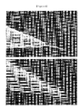
- FIGS. 3 to 7 are SEM pictures in each process of forming the nano electrode of FIG. 1 according to the order of FIG. 2 .
- the main body 100 including the probe 200 is prepared (S10).
- the probe may be formed by electrochemically etching a tungsten wire or depositing the silicon nitride film on the main body 100 and etching the silicon nitride film so as to have a sharp end shape, and then depositing the metal.
- the nano wire 300 is attached to the end of the probe 200 (S20).
- an upper end image of FIG. 3 is obtained by attaching the nano wire to a probe for SPM
- a lower end image of FIG. 3 is a picture obtained by attaching the nano wire to a probe for AFM.
- the nano wire 300 may be attached to the probe by a method such as dielectrophoresis where a strong electric field is applied to a solution including the carbon nano tube or the conductive polymer (for example, polypyrrole and polyaniline).
- a method such as dielectrophoresis where a strong electric field is applied to a solution including the carbon nano tube or the conductive polymer (for example, polypyrrole and polyaniline).
- the insulation material is deposited to cover the nano wire 300 and thus, as illustrated in FIG. 4 , to form the insulation film 400 (S30).
- the insulation film may be formed by a chemical vapor deposition method, or by dipping the nano wire in a liquid type insulation material to coat an external wall of the nano wire with the insulation material.
- the size of the nano electrode may be reduced by minimizing the thickness of the insulation film.
- the thickness of the insulation film 400 is reduced, the size of the nano electrode is reduced but an insulation characteristic of the nano electrode is reduced, and thus it is preferable that the insulation film 400 be formed in a thickness of 500 nm or more in order to maintain the insulation characteristic.
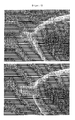
- Cutting may be performed by using a focused ion beam (FIB) using a focused high energy beam such as a laser, or using resistance heat generated if a current is applied in a state where the probe is connected to both sides of the nano wire, or the nano wire may be cut by positioning the nano wire on a hot wire to remove the insulation film by heat of the hot wire.
- FIB focused ion beam
- a focused high energy beam such as a laser
- FIGS. 5 and 6 are pictures in the case where cutting is performed by using the focused ion beam in which the current value is 50 pA, and cutting is performed for 1 minute. Referring to FIGS. 5 and 6 , it can be confirmed that the cross section of the nano wire is exposed at a cut portion.
- the nano electrode is completed by forming the electrode 500 on the cross section of the nano wire 300 by plating (S50). Since plating is performed on only the cross section of the nano wire, the electrode is formed to protrude as compared to the insulation film.
- Plating may be performed by gold, platinum, aluminum, nickel, or the like. In the exemplary embodiment of the present invention, plating is performed in 10 mM K 2 PtCl 4 solution for 2 minutes.
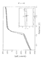
- the nano electrode can be used as the electrode through FIG. 8 .
- FIG. 8 is a graph obtained by measuring CV (cyclic voltammetry) of the nano electrode formed according to the exemplary embodiment of the present invention.
- CV cyclic voltammetry
- a mixture solution of 10 mM ferricyanide compound and 0.5 M KCl is used as the aforementioned solution, and an oxidation reduction reaction of the mixture solution occurs at -0.4 V to -0.3 V.
- the nano electrode according to the present invention may be used as an electrochemical electrode measuring an electrochemical reaction.
Landscapes
- Health & Medical Sciences (AREA)
- General Health & Medical Sciences (AREA)
- General Physics & Mathematics (AREA)
- Nuclear Medicine, Radiotherapy & Molecular Imaging (AREA)
- Radiology & Medical Imaging (AREA)
- Physics & Mathematics (AREA)
- Engineering & Computer Science (AREA)
- Chemical & Material Sciences (AREA)
- Nanotechnology (AREA)
- Manufacturing & Machinery (AREA)
- Measurement And Recording Of Electrical Phenomena And Electrical Characteristics Of The Living Body (AREA)
- Carbon And Carbon Compounds (AREA)
- Micromachines (AREA)
Applications Claiming Priority (2)
| Application Number | Priority Date | Filing Date | Title |
|---|---|---|---|
| KR1020110108858A KR101265776B1 (ko) | 2011-10-24 | 2011-10-24 | 나노 전극 및 그 제조 방법 |
| PCT/KR2012/008663 WO2013062275A1 (fr) | 2011-10-24 | 2012-10-22 | Nanoélectrode et procédé de fabrication de cette dernière |
Publications (2)
| Publication Number | Publication Date |
|---|---|
| EP2772765A1 true EP2772765A1 (fr) | 2014-09-03 |
| EP2772765A4 EP2772765A4 (fr) | 2015-06-03 |
Family
ID=48168048
Family Applications (1)
| Application Number | Title | Priority Date | Filing Date |
|---|---|---|---|
| EP12844016.1A Withdrawn EP2772765A4 (fr) | 2011-10-24 | 2012-10-22 | Nanoélectrode et procédé de fabrication de cette dernière |
Country Status (6)
| Country | Link |
|---|---|
| US (1) | US20140262433A1 (fr) |
| EP (1) | EP2772765A4 (fr) |
| JP (1) | JP6016932B2 (fr) |
| KR (1) | KR101265776B1 (fr) |
| CN (1) | CN104011549A (fr) |
| WO (1) | WO2013062275A1 (fr) |
Families Citing this family (8)
| Publication number | Priority date | Publication date | Assignee | Title |
|---|---|---|---|---|
| US10732201B2 (en) * | 2014-04-13 | 2020-08-04 | Infineon Technologies Ag | Test probe and method of manufacturing a test probe |
| US20180010266A1 (en) * | 2015-01-30 | 2018-01-11 | The Regents Of The University Of California | Method for thermally drawing nanocomposite-enabled multifunctional fibers |
| US9465048B1 (en) * | 2015-03-24 | 2016-10-11 | Inotera Memories, Inc. | Probe unit for test tools and method of manufacturing the same |
| US11543429B2 (en) | 2019-04-25 | 2023-01-03 | Morgan State University | Nanoscale scanning electrochemical microscopy electrode method |
| CN110777424B (zh) * | 2019-11-14 | 2023-07-18 | 南京工业职业技术学院 | 一种纳米针尖批量生产装置及制备方法 |
| CN116519759B (zh) * | 2023-03-23 | 2024-07-16 | 清华大学 | 微电极及单颗粒电极 |
| KR20250054438A (ko) * | 2023-10-16 | 2025-04-23 | 동아대학교 산학협력단 | 전기화학적 분석을 위한 초미세전극 및 이의 제조방법 |
| KR20250131988A (ko) * | 2024-02-28 | 2025-09-04 | 동아대학교 산학협력단 | 전기화학적 분석을 위한 2 채널 초미세전극 및 이의 제조방법 |
Family Cites Families (11)
| Publication number | Priority date | Publication date | Assignee | Title |
|---|---|---|---|---|
| JPH0972926A (ja) * | 1995-09-05 | 1997-03-18 | Nikon Corp | カンチレバー及びその製造方法、並びに前記カンチレバーを用いた走査型プローブ顕微鏡 |
| JP2000516708A (ja) * | 1996-08-08 | 2000-12-12 | ウィリアム・マーシュ・ライス・ユニバーシティ | ナノチューブ組立体から作製された巨視的操作可能なナノ規模の装置 |
| JP4446667B2 (ja) * | 2003-02-14 | 2010-04-07 | 敬義 丹司 | Cnt(カーボンナノチューブ)チップ及びその製造方法、並びに電子銃及び走査型プローブ顕微鏡用探針 |
| WO2004102582A1 (fr) * | 2003-03-05 | 2004-11-25 | University Of Florida | Sondes a base de nanotubes de carbone, dispositifs apparentes et procedes pour realiser ces sondes |
| JP2007527507A (ja) * | 2003-07-08 | 2007-09-27 | キューナノ エービー | ナノウィスカーを組み込んだプローブ構造体、その製造方法及びナノウィスカーを形成する方法 |
| US20080098805A1 (en) * | 2004-10-06 | 2008-05-01 | Sungho Jin | Nanotube-Based Nanoprobe Structure and Method for Making the Same |
| US7435353B2 (en) * | 2004-12-09 | 2008-10-14 | President And Fellows Of Harvard College | Patterning by energetically-stimulated local removal of solid-condensed-gas layers and solid state chemical reactions produced with such layers |
| KR100697323B1 (ko) * | 2005-08-19 | 2007-03-20 | 한국기계연구원 | 나노 팁 및 이의 제조방법 |
| KR101159074B1 (ko) * | 2006-01-14 | 2012-06-25 | 삼성전자주식회사 | 도전성 탄소나노튜브 팁, 이를 구비한 스캐닝 프로브마이크로스코프의 탐침 및 상기 도전성 탄소나노튜브 팁의제조 방법 |
| US7572300B2 (en) * | 2006-03-23 | 2009-08-11 | International Business Machines Corporation | Monolithic high aspect ratio nano-size scanning probe microscope (SPM) tip formed by nanowire growth |
| US7601650B2 (en) * | 2007-01-30 | 2009-10-13 | Carbon Design Innovations, Inc. | Carbon nanotube device and process for manufacturing same |
-
2011
- 2011-10-24 KR KR1020110108858A patent/KR101265776B1/ko not_active Expired - Fee Related
-
2012
- 2012-10-22 EP EP12844016.1A patent/EP2772765A4/fr not_active Withdrawn
- 2012-10-22 US US14/353,795 patent/US20140262433A1/en not_active Abandoned
- 2012-10-22 JP JP2014538701A patent/JP6016932B2/ja not_active Expired - Fee Related
- 2012-10-22 CN CN201280064051.XA patent/CN104011549A/zh active Pending
- 2012-10-22 WO PCT/KR2012/008663 patent/WO2013062275A1/fr not_active Ceased
Also Published As
| Publication number | Publication date |
|---|---|
| US20140262433A1 (en) | 2014-09-18 |
| JP2015502521A (ja) | 2015-01-22 |
| JP6016932B2 (ja) | 2016-10-26 |
| EP2772765A4 (fr) | 2015-06-03 |
| CN104011549A (zh) | 2014-08-27 |
| KR101265776B1 (ko) | 2013-05-20 |
| KR20130044674A (ko) | 2013-05-03 |
| WO2013062275A1 (fr) | 2013-05-02 |
Similar Documents
| Publication | Publication Date | Title |
|---|---|---|
| EP2772765A1 (fr) | Nanoélectrode et procédé de fabrication de cette dernière | |
| EP1290431B1 (fr) | Procede pour la production d'un dispositif permettant l'execution simultanee d'une microscopie a champ proche electrochimique et topographique | |
| Nellist et al. | Atomic force microscopy with nanoelectrode tips for high resolution electrochemical, nanoadhesion and nanoelectrical imaging | |
| US7964143B2 (en) | Nanotube device and method of fabrication | |
| US7824620B2 (en) | Nano- and micro-scale structures: methods, devices and applications thereof | |
| CN101176167A (zh) | 用于电化学、电学或形貌分析的传感器 | |
| Lugstein et al. | Integrating micro-and nanoelectrodes into atomic force microscopy cantilevers using focused ion beam techniques | |
| US8168251B2 (en) | Method for producing tapered metallic nanowire tips on atomic force microscope cantilevers | |
| Pust et al. | Influence of electrode size and geometry on electrochemical experiments with combined SECM–SFM probes | |
| Knittel et al. | Challenges in nanoelectrochemical and nanomechanical studies of individual anisotropic gold nanoparticles | |
| WO2012072507A1 (fr) | Capteur afm-secm | |
| TWI472774B (zh) | 探針針尖修飾方法 | |
| Salomo et al. | Integrated cantilever probes for SECM/AFM characterization of surfaces | |
| Woo et al. | Fabrication of nanoscale gold disk electrodes using ultrashort pulse etching | |
| Dobson et al. | Electron beam lithographically-defined scanning electrochemical-atomic force microscopy probes: fabrication method and application to high resolution imaging on heterogeneously active surfaces | |
| Sripirom et al. | Easily made and handled carbon nanocones for scanning tunneling microscopy and electroanalysis | |
| CN115901888A (zh) | 一种利用二维平面纳米导电材料侧面的电化学一维纳米电极及其制备方法与应用 | |
| US20190376928A1 (en) | Electrochemical Stripping Analysis Using Vertically Free Standing Graphene containing Carbon Nanosheets as Electrode Materials | |
| Yun et al. | Dielectric breakdown and post-breakdown dissolution of Si/SiO2 cathodes in acidic aqueous electrochemical environment | |
| Baumeister et al. | Scanning Tunneling Microscopy II: Further Applications and Related Scanning Techniques | |
| US10879034B2 (en) | Membraneless platform for correlated analysis of nanomaterials | |
| KR101343012B1 (ko) | 나노 전극 및 그 제조 방법 | |
| Zhu et al. | Insulating method using cataphoretic paint for tungsten tips for electrochemical scanning tunnelling microscopy (ECSTM) | |
| Moon et al. | Bitmap-assisted focused ion beam fabrication of combined atomic force scanning electrochemical microscopy probes | |
| Narui et al. | High aspect ratio silicon dioxide-coated single-walled carbon nanotube scanning probe nanoelectrodes |
Legal Events
| Date | Code | Title | Description |
|---|---|---|---|
| PUAI | Public reference made under article 153(3) epc to a published international application that has entered the european phase |
Free format text: ORIGINAL CODE: 0009012 |
|
| 17P | Request for examination filed |
Effective date: 20140429 |
|
| AK | Designated contracting states |
Kind code of ref document: A1 Designated state(s): AL AT BE BG CH CY CZ DE DK EE ES FI FR GB GR HR HU IE IS IT LI LT LU LV MC MK MT NL NO PL PT RO RS SE SI SK SM TR |
|
| DAX | Request for extension of the european patent (deleted) | ||
| RA4 | Supplementary search report drawn up and despatched (corrected) |
Effective date: 20150507 |
|
| RIC1 | Information provided on ipc code assigned before grant |
Ipc: G01Q 70/12 20100101AFI20150429BHEP |
|
| 17Q | First examination report despatched |
Effective date: 20171026 |
|
| STAA | Information on the status of an ep patent application or granted ep patent |
Free format text: STATUS: THE APPLICATION IS DEEMED TO BE WITHDRAWN |
|
| 18D | Application deemed to be withdrawn |
Effective date: 20180306 |