EP2772834A2 - Dispositif de vitre tactile et méthode de fabrication dudit dispositif - Google Patents
Dispositif de vitre tactile et méthode de fabrication dudit dispositif Download PDFInfo
- Publication number
- EP2772834A2 EP2772834A2 EP20120182157 EP12182157A EP2772834A2 EP 2772834 A2 EP2772834 A2 EP 2772834A2 EP 20120182157 EP20120182157 EP 20120182157 EP 12182157 A EP12182157 A EP 12182157A EP 2772834 A2 EP2772834 A2 EP 2772834A2
- Authority
- EP
- European Patent Office
- Prior art keywords
- touch
- layer
- lens
- lens device
- manufacturing
- Prior art date
- Legal status (The legal status is an assumption and is not a legal conclusion. Google has not performed a legal analysis and makes no representation as to the accuracy of the status listed.)
- Withdrawn
Links
Images




Classifications
-
- G—PHYSICS
- G06—COMPUTING OR CALCULATING; COUNTING
- G06F—ELECTRIC DIGITAL DATA PROCESSING
- G06F3/00—Input arrangements for transferring data to be processed into a form capable of being handled by the computer; Output arrangements for transferring data from processing unit to output unit, e.g. interface arrangements
- G06F3/01—Input arrangements or combined input and output arrangements for interaction between user and computer
- G06F3/03—Arrangements for converting the position or the displacement of a member into a coded form
- G06F3/041—Digitisers, e.g. for touch screens or touch pads, characterised by the transducing means
-
- G—PHYSICS
- G06—COMPUTING OR CALCULATING; COUNTING
- G06F—ELECTRIC DIGITAL DATA PROCESSING
- G06F3/00—Input arrangements for transferring data to be processed into a form capable of being handled by the computer; Output arrangements for transferring data from processing unit to output unit, e.g. interface arrangements
- G06F3/01—Input arrangements or combined input and output arrangements for interaction between user and computer
- G06F3/03—Arrangements for converting the position or the displacement of a member into a coded form
- G06F3/041—Digitisers, e.g. for touch screens or touch pads, characterised by the transducing means
- G06F3/044—Digitisers, e.g. for touch screens or touch pads, characterised by the transducing means by capacitive means
- G06F3/0446—Digitisers, e.g. for touch screens or touch pads, characterised by the transducing means by capacitive means using a grid-like structure of electrodes in at least two directions, e.g. using row and column electrodes
-
- B—PERFORMING OPERATIONS; TRANSPORTING
- B32—LAYERED PRODUCTS
- B32B—LAYERED PRODUCTS, i.e. PRODUCTS BUILT-UP OF STRATA OF FLAT OR NON-FLAT, e.g. CELLULAR OR HONEYCOMB, FORM
- B32B33/00—Layered products characterised by particular properties or particular surface features, e.g. particular surface coatings; Layered products designed for particular purposes not covered by another single class
-
- G—PHYSICS
- G06—COMPUTING OR CALCULATING; COUNTING
- G06F—ELECTRIC DIGITAL DATA PROCESSING
- G06F3/00—Input arrangements for transferring data to be processed into a form capable of being handled by the computer; Output arrangements for transferring data from processing unit to output unit, e.g. interface arrangements
- G06F3/01—Input arrangements or combined input and output arrangements for interaction between user and computer
- G06F3/03—Arrangements for converting the position or the displacement of a member into a coded form
- G06F3/041—Digitisers, e.g. for touch screens or touch pads, characterised by the transducing means
- G06F3/044—Digitisers, e.g. for touch screens or touch pads, characterised by the transducing means by capacitive means
- G06F3/0443—Digitisers, e.g. for touch screens or touch pads, characterised by the transducing means by capacitive means using a single layer of sensing electrodes
-
- B—PERFORMING OPERATIONS; TRANSPORTING
- B32—LAYERED PRODUCTS
- B32B—LAYERED PRODUCTS, i.e. PRODUCTS BUILT-UP OF STRATA OF FLAT OR NON-FLAT, e.g. CELLULAR OR HONEYCOMB, FORM
- B32B2457/00—Electrical equipment
- B32B2457/20—Displays, e.g. liquid crystal displays, plasma displays
- B32B2457/208—Touch screens
-
- G—PHYSICS
- G06—COMPUTING OR CALCULATING; COUNTING
- G06F—ELECTRIC DIGITAL DATA PROCESSING
- G06F2203/00—Indexing scheme relating to G06F3/00 - G06F3/048
- G06F2203/041—Indexing scheme relating to G06F3/041 - G06F3/045
- G06F2203/04103—Manufacturing, i.e. details related to manufacturing processes specially suited for touch sensitive devices
-
- Y—GENERAL TAGGING OF NEW TECHNOLOGICAL DEVELOPMENTS; GENERAL TAGGING OF CROSS-SECTIONAL TECHNOLOGIES SPANNING OVER SEVERAL SECTIONS OF THE IPC; TECHNICAL SUBJECTS COVERED BY FORMER USPC CROSS-REFERENCE ART COLLECTIONS [XRACs] AND DIGESTS
- Y10—TECHNICAL SUBJECTS COVERED BY FORMER USPC
- Y10T—TECHNICAL SUBJECTS COVERED BY FORMER US CLASSIFICATION
- Y10T428/00—Stock material or miscellaneous articles
- Y10T428/24—Structurally defined web or sheet [e.g., overall dimension, etc.]
- Y10T428/24802—Discontinuous or differential coating, impregnation or bond [e.g., artwork, printing, retouched photograph, etc.]
-
- Y—GENERAL TAGGING OF NEW TECHNOLOGICAL DEVELOPMENTS; GENERAL TAGGING OF CROSS-SECTIONAL TECHNOLOGIES SPANNING OVER SEVERAL SECTIONS OF THE IPC; TECHNICAL SUBJECTS COVERED BY FORMER USPC CROSS-REFERENCE ART COLLECTIONS [XRACs] AND DIGESTS
- Y10—TECHNICAL SUBJECTS COVERED BY FORMER USPC
- Y10T—TECHNICAL SUBJECTS COVERED BY FORMER US CLASSIFICATION
- Y10T428/00—Stock material or miscellaneous articles
- Y10T428/26—Web or sheet containing structurally defined element or component, the element or component having a specified physical dimension
-
- Y—GENERAL TAGGING OF NEW TECHNOLOGICAL DEVELOPMENTS; GENERAL TAGGING OF CROSS-SECTIONAL TECHNOLOGIES SPANNING OVER SEVERAL SECTIONS OF THE IPC; TECHNICAL SUBJECTS COVERED BY FORMER USPC CROSS-REFERENCE ART COLLECTIONS [XRACs] AND DIGESTS
- Y10—TECHNICAL SUBJECTS COVERED BY FORMER USPC
- Y10T—TECHNICAL SUBJECTS COVERED BY FORMER US CLASSIFICATION
- Y10T428/00—Stock material or miscellaneous articles
- Y10T428/31504—Composite [nonstructural laminate]
- Y10T428/31721—Of polyimide
Definitions
- the present disclosure relates to a touch device, and more particularly to a touch-on-lens (TOL) device and a method for manufacturing the same.
- TOL touch-on-lens
- a capacitive touch device generally comprises X-axis and Y-axis transparent electrodes. When a user touches the device, capacitance of touch point changes and a system determines location of the touch point by detecting the change in capacitance.
- FIG. 1A shows a schematic stacked view of a conventional capacitive touch device that mainly comprises of a cover lens 11 and a touch substrate 12.
- a touch layer which comprises of transparent electrodes, is formed at either a single side or both sides of the touch substrate 12.
- FIG. 1B shows a schematic stacked view of a conventional touch-on-lens (TOL) device that leaves out the a touch substrate and directly disposes a touch layer 13, such as an ITO layer, on a cover lens 11 without adding a glass substrate so as to make the touch device thinner.
- TOL touch-on-lens
- the first method includes: strengthening a small piece of lens, namely a piece of lens that meets size of a touch panel, and then stacking a touch unit and other stack structures on the lens through a photoetching process.
- the second method includes: stacking a touch layer and other stack structures on a large-size motherboard of strengthened glass through a photoetching process, and then cutting the glass motherboard into a touch panel with a specific size through a process of glass motherboard cutting and edge polishing, etc.
- the above-mentioned two methods have some defects; for example, for the first method, cost of a single piece output is very high and efficiency of mass production is low, that do not meet economic benefit. Comparing with the first method, cost of single piece output for the second method is comparatively low and efficiency of mass production is comparatively high, but for the touch panel after cutting process, mechanical property of the glass is weakened because of no edge strengthening process.
- a sensing pattern of a touch layer on a PET (ethylene terephthalate) film through a printing process so as to form a PET touch motherboard; and then, cutting the PET touch motherboard into a touch panel with a specific size so as to form a touch sub-panel; and finally, laminating the touch sub-panel on the strengthened lens of corresponding size.
- this manufacturing process is high in efficiency of mass production and good in mechanical property.
- a touch sensing pattern is formed on a PET film generally through a printing process rather than through a photoetching process.
- line width of the touch sensing pattern formed by the printing method is comparatively wide due to an influence of the printing device, printing ink, and printing technique, etc., that makes the circuit visible and affects appearance of the product.
- generally thickness of a PET film is 25 ⁇ m-350 ⁇ m, which reduces the capability of making the touch panel thinner.
- An object of the embodiments of the present disclosure is to provide a touch-on-lens (TOL) device and a method for manufacturing the same, forming a touch layer with a large area on a plastic layer through a photoetching process and improving existing problems of low efficiency of mass production of touch-on-lens devices, bad mechanical strength, and circuit visibility, etc. through a cutting technique.
- TOL touch-on-lens
- a method for manufacturing a touch-on-lens device comprises the following steps: (1) forming a plastic layer on a substrate; (2) forming a touch layer on the plastic layer such that the touch layer and the plastic layer form a touch film; (3) separating the touch film and the substrate; (4) cutting the touch film to form a plurality of touch modules; and (5) laminating the touch modules to a strengthened lens.
- the plastic layer is a polyimide (PI) layer or a polyesterimide layer.
- PI polyimide
- the touch layer comprises a sensing pattern, which is formed by a photoetching process.
- the touch-on-lens device further comprises a release layer, which is formed between a plastic layer and a substrate and is made up of a silicon-based or a F-based compound.
- adhesive strength between the substrate and the release layer is at least three times the adhesive strength between the release layer and the plastic layer.
- the touch film comprises a buffer layer that is formed between the touch layer and the plastic layer and is made up of derivative or compound of silicon.
- thickness of the plastic layer is less than 25 ⁇ m.
- a method for manufacturing a touch-on-lens device further comprises forming a mask layer on strengthened lens, wherein the mask layer and the touch modules are at a same side of the strengthened lens.
- a method for manufacturing a touch-on-lens device comprises the following steps: (1) forming a plastic layer on a motherboard; (2) forming a touch layer on the plastic layer so that the motherboard, the plastic layer, and the touch layer form a touch assembly; (3) cutting the touch assembly to form a plurality of touch sub-assemblies; (4) laminating the touch sub-assemblies to a strengthened lens; and (5) separating the motherboard after cutting.
- the plastic layer is a polyimide (PI) layer or a polyesterimide layer.
- the touch layer comprises a sensing pattern, which is formed by a photoetching process.
- the touch assembly further comprises a release layer, that is formed between the plastic layer and the motherboard and is made up of silicon-based or F-based compound.
- the touch assembly further comprises a buffer layer, which is formed between the touch layer and the plastic layer and is made up of derivative or compound of silicon. Further, the plastic layer and the touch layer of the touch assembly constitute a touch film.
- the touch sub-assembly comprises the motherboard and a touch module which is formed after cutting the touch film.
- the lamination process of step (4) further comprises laminating the touch modules of the touch sub-assemblies to the strengthened lens.
- the method for manufacturing a touch-on-lens device further comprises forming a mask layer on strengthened lens, wherein the mask layer and the touch modules are at the same side of the strengthened lens.
- a touch-on-lens device comprises: a strengthened lens; and a touch module, that is laminated to the strengthened lens and formed by cutting a touch film, wherein the touch film comprises of a touch layer and a plastic layer, further wherein thickness of the plastic layer is less than 25 ⁇ m.
- thickness of the plastic layer is between 10 ⁇ m - 20 ⁇ m.
- thickness of the plastic layer is between 0.5 ⁇ m - 10 ⁇ m.
- the plastic layer is a polyimide (PI) layer or a polyesterimide layer.
- the touch layer comprises a sensing pattern, which is formed by a photoetching process.
- the touch film further comprises a buffer layer, which is formed between the touch layer and the plastic layer and is made up of derivative or compound of silicon.
- the touch-on-lens device further comprises a mask layer, wherein the mask layer and the touch module are formed at the same side of the strengthened lens.
- the present disclosure adopts the above method, namely, first forming a plastic layer on a substrate, and then forming a touch layer on the plastic layer and finally laminating the touch layer after cutting to a strengthened lens, and since the present disclosure adopts the method of cutting first and then laminating the touch layer, the present method can not only keep good mechanical property but can also enhance efficiency of mass production. Moreover, the present disclosure adopts a photoetching process to form a sensing pattern, which can make the circuit thinner so as to beautify the appearance.
- FIG. 1A shows a schematic stacked view of a conventional capacitive touch device
- FIG. 1B shows a schematic stacked view of a conventional touch-on-lens (TOL) device
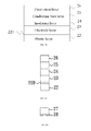
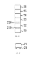
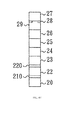
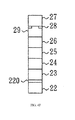
- FIG. 2A to FIG. 2F show schematic stacked views of a touch-on-lens device during the process in accordance with a first embodiment of the present disclosure
- FIG. 3A shows an electrode layer in accordance with the present embodiment
- FIG. 3B shows an insulating layer in accordance with the present embodiment
- FIG. 3C shows a conducting wire layer in accordance with the present embodiment
- FIG. 4A to FIG. 4F show schematic stacked views of a touch-on-lens device during the process in accordance with a second embodiment of the present disclosure.
- FIG. 2A to FIG. 2F show schematic stacked views of a touch-on-lens device during the process in accordance with the first embodiment of the present disclosure.
- the upward side refers to the direction of a touch surface. Thickness of each layer shown in the drawings is not drawn according to the actual proportion. Besides, the drawings only show the main layers in accordance with the embodiments, and other layers can be inserted between the layers according to the actual need.
- a transparent plastic layer 22 is firstly formed on a substrate 21.
- the substrate 21 can be a glass substrate, plastic film, or other hard substrates, and the substrate 21 can be separated from the other parts so that it can be used for other processes again.
- the plastic layer 22 is a polyimide (PI) layer or a polyesterimide layer, but other plastics that are easy to be separated from the substrate can also be used, such as ceramic thin film (such as SiO 2 ).
- PET polyethylene terephthalate
- polyimide (PI) as the material of the plastic layer 22 at least has the following effects: for example, comparatively easy to be separated from the substrate 21 in the future; high-temperature resistance; and good optical characteristics.
- polyesterimide as the material of the plastic layer 22 at least has the following effects: for example, high mechanical strength, high light transmittance or high chemical resistance, which can effectively protect a touch layer (23, 24, 25) from being eroded by a weak acid (such as sweat).
- thickness of the plastic layer 22 is less than 25 ⁇ m. In a more preferred embodiment, thickness of the plastic layer 22 is between 10-22 ⁇ m. In a most preferred embodiment, thickness of the plastic layer 22 is between 0.5 ⁇ m - 10 ⁇ m.
- the device in the present embodiment has a comparatively thin plastic layer 22, and therefore a thinner touch-on-lens (TOL) device can be made.
- the plastic layer 22 can form on the substrate 21, a high contact-angle material, which is deposited or coated on the substrate 21 before forming the plastic layer 22.
- FIG. 3A shows an electrode layer 23 in accordance with the present embodiment, wherein the electrode layer 23 comprises a plurality of first electrodes 23A along a first axis (such as Y-axis) that are connected with each other along the first axis and a plurality of second electrodes 23B along a second axis (such as X-axis) that are not connected with each other.
- Sensing pattern of the electrode layer 23 can be made by a photoetching process.
- the photoetching process comprises photoresist coating, exposure, developing, baking, etching, stripping and other processing steps.
- FIG. 3B shows an insulating layer 24 in accordance with the present embodiment, wherein the insulating layer 24 comprises a plurality of insulating blocks 24A that respectively cover area between adjacent second electrodes 23B along the second axis (such as X-axis).
- FIG. 3C shows a conducting wire layer 25 in accordance with the present embodiment, wherein the conducting wire layer 25 comprises a plurality of wire segments 25A, which are respectively bridged over the insulating blocks 24A to electrically couple the adjacent second electrodes 23B along the second axis (such as X-axis) and a plurality of trace wires 25B, which are used for electrically coupling the first-axis and the second-axis electrodes respectively and extend to the border of the touch-on-lens (TOL) device.
- Pattern of the conducting wire layer 25 can be made by a photoetching process.
- the electrode layer 23, the insulating layer 24, and the conducting wire layer 25 jointly form a single-layer touch layer.
- the single-layer touch layer can also be called as single-layer ITO (SITO).
- the electrode layer 23, the insulating layer 24, and the conducting wire layer 25 constitute a touch layer of the present embodiment, but the touch layer of the present disclosure is not limited to the above composition and arrangement methods.
- the plastic layer 22 and the touch layer (23, 24, 25) form a touch film, wherein the touch layer (23, 24, 25) comprises a plurality of touch units, size of which meets specific size of a touch panel.
- a passivation layer 26 can be formed on a conducting wire layer 25, wherein the passivation layer 26 can not only protect an electrode layer 23, an insulating layer 24, and a conducting wire layer 25 from damage but can also prevent them from getting oxidized or corroded.
- a release layer 210 can be formed between substrate 21 and plastic layer 22, for example, by using a coating technique.
- the release layer 210 can be made of silicon-based or F-based compound, but it is not limited to this.
- the plastic layer 22 is a polyesterimide layer, which is formed by coating (such as spin coating) a monomer on the release layer 210 and then processing through a curing process.
- adhesive strength between the substrate 21 and the release layer 210 is higher than (such as three times) the adhesive strength between the release layer 210 and the plastic layer 22, which makes the plastic layer 22 easy to be separated from the release layer 210 by an external force while the release layer 210 is completely retained on the substrate 21.
- a buffer layer 220 can be formed between plastic layer 22 and electrode layer 23, for example, by using a deposition technique.
- the buffer layer 220 can be made of derivative or compound of silicon, such as silicon nitride or silicon oxide, but it is not limited to this.
- thickness of the buffer layer 220 is 10nm (nanometer) or more than 200nm.
- touch film 22-25 and substrate 21 can be separated to form a structure shown in FIG. 2B .
- the touch film can be cut so that each touch unit forms a touch module and each touch module can form an independent touch panel through a subsequent process.
- the present embodiment forms a plurality of touch units, sizes of which meet the specific size of a touch panel, on a plastic layer 22, and then cut the formed touch units, which contributes to improvement in efficiency of mass production of the touch-on-lens (TOL) device, thereby enhancing productivity.
- TOL touch-on-lens
- a strengthened lens 27 (also referred to as cover lens hereinafter) can additionally be provided, as shown in FIG. 2D .
- the strengthened lens 27 can be made by cutting a glass motherboard into one that meets the size of a touch module, and then by performing an edge polishing. Comparing with the conventional method of cutting the glass after depositing the stacked touch layer, the strengthened lens 27 in the present embodiment has a strengthened edge and mechanical property.
- a mask layer (or a black matrix layer) 28 can be formed on the strengthened lens 27 by a printing technique.
- an adhesive layer 29, such as liquid adhesive, can be used for gluing the two structures together; namely, the upper surface of the adhesive layer 29 can be glued to the lower surface of the strengthened lens 27 and the mask layer 28, and the lower surface of the adhesive layer 29 can be glued to the upper surface of the passivation layer 26.
- the passivation layer 26 is not formed, lower surface of the adhesive layer 29 can be glued to the upper surface of the touch layer (23, 24, 25), that is, the mask layer 28 and the touch module 22-26 can be formed at the same side of the strengthened lens 27.
- stack structure shown in FIG. 2F is formed, namely, the structure from the bottom to the top comprises a plastic layer 22, a buffer layer 220, an electrode layer 23, an insulating layer 24, a conducting wire layer 25, a passivation layer 26, an adhesive layer 29, a mask layer 28, and a strengthened lens 27.
- a touch layer (23, 24, 25) is firstly formed on a plastic layer 22 and then glued to a strengthened lens 27 that has been cut and processed with a high strength. Therefore, the requirement for strength of various end products can be reached and mass production can be carried out.
- the touch-on-lens (TOL) device formed by the above process if ITO is used as the material of the electrode layer 23, and polyimide (PI) is used as the material of the plastic layer 22, the process is suitable for making a curved-surface touch-on-lens device as adhesiveness of the two materials is very good and not easy to crack.
- the conducting wire layer 25 does not contact with the mask layer 28 directly, and therefore there will be no open circuit problem unlike the conventional problem of an open circuit being formed by height difference of the mask layer 28.
- FIG. 4A to FIG. 4F show schematic stacked views of a touch-on-lens device during the process in accordance with a second embodiment of the present disclosure.
- the present embodiment is similar to the first embodiment (as shown in FIG. 2A to FIG. 2F ), in terms of the materials, thickness, manufacturing process and other effects.
- a transparent plastic layer 22 is firstly formed on a motherboard 20.
- the motherboard 20 can be glass substrate, plastic film or other hard substrates, and the motherboard 20 can be separated from the other parts.
- a transparent electrode layer 23, a transparent insulating layer 24, and a conducting wire layer 25 are formed on the plastic layer 22 in sequence.
- the electrode layer 23, the insulating layer 24, and the conducting wire layer 25 constitute a touch layer of the present embodiment.
- the motherboard 20, the plastic layer 22, and the touch layer (23, 24, 25) form a touch assembly, wherein the touch layer (23, 24, 25) comprises a plurality of touch units.
- a passivation layer 26 can also be formed on the conducting wire layer 25, which can not only protect the electrode layer 23, the insulating layer 24, and the conducting wire layer 25 from damage but can also prevent them from getting oxidized or corroded.
- a release layer 210 can also be formed between the motherboard 20 and the plastic layer 22, and a buffer layer 220 can also be formed between the plastic layer 22 and the electrode layer 23.
- the touch assembly can be cut so that each touch unit forms an independent touch sub-assembly. Comparing with the conventional method of manufacturing one unit by one unit, the present embodiment firstly forms a plurality of touch units and then cuts them, which contributes to increasing possibility of mass production of the touch-on-lens (TOL) device and to enhancing productivity.
- TOL touch-on-lens
- a strengthened lens 27 can additionally be provided, as shown in FIG. 4C .
- a mask layer 28 can be formed under the strengthened lens 27.
- an adhesive layer 29 can be used for gluing the two structures together; namely, the upper surface of the adhesive layer 29 can be glued to the lower surfaces of the strengthened lens 27 and the mask layer 28, and the lower surface of the adhesive layer 29 can be glued to the upper surface of the passivation layer 26. If the passivation layer 26 is not formed, the lower surface of the adhesive layer 29 can be glued to the upper surface of the touch layer (23, 24, 25). After gluing, the stack structure shown in FIG.
- the structure from bottom to top comprises a motherboard 20, a release layer 210, a plastic layer 22, a buffer layer 220, an electrode layer 23, an insulating layer 24, a conducting wire layer 25, a passivation layer 26, an adhesive layer 29, a mask layer 28, and a strengthened lens 27.
- the motherboard 20 is separated from the structure as shown in FIG. 4E , forming the structure as shown in FIG. 4F .
- the touch device comprises a strengthened lens 27 and a touch module (22, 220, 23, 24, 25, 26), wherein the touch module is laminated to the strengthened lens 27.
- the touch module is formed by cutting a touch film that comprises a touch layer (23, 24, 25) and a plastic layer 22, wherein thickness of the plastic layer is less than 25 ⁇ m.
- the plastic layer is a polyimide (PI) layer or a polyesterimide layer; the plastic layer is high-temperature resistant with good optical characteristics, and its thickness can be controlled within a comparatively thin scope.
- thickness of the plastic layer 22 is 10-20 ⁇ m. In a more preferred embodiment, thickness of the plastic layer 22 is 0.5-10 ⁇ m. Comparing with other plastic layers, such as PET, using the plastic layer can further make the touch-on-lens device thinner.
Landscapes
- Engineering & Computer Science (AREA)
- General Engineering & Computer Science (AREA)
- Theoretical Computer Science (AREA)
- Human Computer Interaction (AREA)
- Physics & Mathematics (AREA)
- General Physics & Mathematics (AREA)
- Position Input By Displaying (AREA)
- Solid State Image Pick-Up Elements (AREA)
Applications Claiming Priority (1)
| Application Number | Priority Date | Filing Date | Title |
|---|---|---|---|
| CN201110269450.7A CN102968200B (zh) | 2011-09-01 | 2011-09-01 | 镜片触控装置及其制程方法 |
Publications (2)
| Publication Number | Publication Date |
|---|---|
| EP2772834A2 true EP2772834A2 (fr) | 2014-09-03 |
| EP2772834A3 EP2772834A3 (fr) | 2014-10-08 |
Family
ID=46723234
Family Applications (1)
| Application Number | Title | Priority Date | Filing Date |
|---|---|---|---|
| EP20120182157 Withdrawn EP2772834A3 (fr) | 2011-09-01 | 2012-08-29 | Dispositif de vitre tactile et méthode de fabrication dudit dispositif |
Country Status (6)
| Country | Link |
|---|---|
| US (1) | US20130059128A1 (fr) |
| EP (1) | EP2772834A3 (fr) |
| JP (1) | JP5838131B2 (fr) |
| KR (1) | KR101430596B1 (fr) |
| CN (1) | CN102968200B (fr) |
| TW (2) | TWM431427U (fr) |
Families Citing this family (11)
| Publication number | Priority date | Publication date | Assignee | Title |
|---|---|---|---|---|
| KR101774211B1 (ko) * | 2012-01-18 | 2017-09-04 | 미쯔비시 케미컬 주식회사 | 화상 표시 장치용 투명 양면 점착 시트 및 이를 사용한 화상 표시 장치 |
| TWI474236B (zh) * | 2012-10-11 | 2015-02-21 | Touchplus Information Corp | 觸控面板以及其感測墊配置方法 |
| CN103257774B (zh) * | 2013-05-10 | 2016-01-20 | 深圳市立德通讯器材有限公司 | 一种ogs电容触摸屏及其制造方法 |
| CN103309538B (zh) * | 2013-06-19 | 2016-05-25 | 南昌欧菲光学技术有限公司 | 电容式触摸屏制备方法 |
| CN104516576B (zh) | 2013-09-29 | 2016-04-13 | 宸鸿科技(厦门)有限公司 | 触控面板的制作方法 |
| CN103870015A (zh) * | 2014-03-20 | 2014-06-18 | 汕头超声显示器技术有限公司 | 一种电容触摸屏制造方法 |
| TWI515628B (zh) * | 2014-06-17 | 2016-01-01 | 恆顥科技股份有限公司 | 觸控顯示器 |
| US20160147323A1 (en) * | 2014-11-21 | 2016-05-26 | Interface Optoelectronics Corporation | Touch control panel structure and method of manufacturing the same |
| TWI685781B (zh) * | 2016-09-20 | 2020-02-21 | 日商凸版印刷股份有限公司 | 顯示裝置及顯示裝置基板 |
| CN106597725A (zh) * | 2017-02-06 | 2017-04-26 | 京东方科技集团股份有限公司 | 一种显示装置及其制作方法、制作设备 |
| CN113221753B (zh) * | 2021-05-14 | 2023-12-29 | 业泓科技(成都)有限公司 | 触控感测模组的制作方法及触控感测模组母板 |
Citations (7)
| Publication number | Priority date | Publication date | Assignee | Title |
|---|---|---|---|---|
| US20040038515A1 (en) * | 2001-11-30 | 2004-02-26 | Siegel Harry M. | Method of making a semiconductor device having a planarized fluoropolymer passivating layer with selectively implanted charged particles |
| US20070059854A1 (en) * | 2005-09-14 | 2007-03-15 | Chin-Jen Huang | Flexible pixel array substrate and method for fabricating the same |
| EP1986084A1 (fr) * | 2007-04-27 | 2008-10-29 | TPK Touch Solutions Inc. | Structure de motif conducteur de panneau tactile capacitif |
| US20090322702A1 (en) * | 2008-06-25 | 2009-12-31 | Au Optronics Corporation | Touch sensing display panel, touch sensing color filter and fabricating method thereof |
| US20090324899A1 (en) * | 2008-06-30 | 2009-12-31 | Feinstein Casey J | Full perimeter chemical strengthening of substrates |
| US20100103138A1 (en) * | 2008-10-27 | 2010-04-29 | Tpk Touch Solutions Inc. | Curved capacitive touch panel and manufacture method thereof |
| EP2354900A2 (fr) * | 2008-11-14 | 2011-08-10 | LG Innotek Co., Ltd. | Écran tactile et son procédé de fabrication |
Family Cites Families (24)
| Publication number | Priority date | Publication date | Assignee | Title |
|---|---|---|---|---|
| JPH01319210A (ja) * | 1988-06-17 | 1989-12-25 | Ricoh Co Ltd | ポリマーフィルム基板における透明電極形成方法 |
| US5062916A (en) * | 1990-08-01 | 1991-11-05 | W. H. Brady Co. | Method for the manufacture of electrical membrane panels having circuits on flexible plastic films |
| US5395740A (en) * | 1993-01-27 | 1995-03-07 | Motorola, Inc. | Method for fabricating electrode patterns |
| JP3110652B2 (ja) * | 1995-05-31 | 2000-11-20 | シャープ株式会社 | マイクロレンズ基板及びそれを用いた液晶表示素子 |
| EP0782039A3 (fr) * | 1995-12-27 | 1998-06-17 | Canon Kabushiki Kaisha | Dispositif d'affichage et son procédé de fabrication |
| US6718612B2 (en) * | 1999-08-04 | 2004-04-13 | Asahi Glass Company, Ltd. | Method for manufacturing a magnetic disk comprising a glass substrate using a protective layer over a glass workpiece |
| US6819316B2 (en) * | 2001-04-17 | 2004-11-16 | 3M Innovative Properties Company | Flexible capacitive touch sensor |
| JP4118708B2 (ja) * | 2003-02-28 | 2008-07-16 | アルプス電気株式会社 | フレキシブルセンサおよびそれを用いた入力装置並びにフレキシブルセンサの製造方法 |
| JP2005031790A (ja) * | 2003-07-08 | 2005-02-03 | Alps Electric Co Ltd | 静電容量式入力センサの実装方法および電子機器 |
| JP4438381B2 (ja) * | 2003-11-05 | 2010-03-24 | 株式会社ブリヂストン | 結晶性ito膜、ito膜の結晶化方法、透明導電性フィルム、タッチパネル及び色素増感型太陽電池 |
| JP4133787B2 (ja) * | 2003-12-17 | 2008-08-13 | Tdk株式会社 | 転写用機能性フィルム、機能性層の形成方法、及び機能性層が付与された物体 |
| US8610690B2 (en) * | 2007-07-27 | 2013-12-17 | Tpk Touch Solutions Inc. | Capacitive sensor and method for manufacturing same |
| TWI528249B (zh) * | 2009-04-15 | 2016-04-01 | 財團法人工業技術研究院 | 觸控裝置之結構 |
| TWM363641U (en) * | 2009-04-21 | 2009-08-21 | Emerging Display Tech Corp | Capacitive touch input device |
| US20110005662A1 (en) * | 2009-07-10 | 2011-01-13 | Kuo-Hua Sung | Method for Fabricating Multilayer Panels |
| US20110012845A1 (en) * | 2009-07-20 | 2011-01-20 | Rothkopf Fletcher R | Touch sensor structures for displays |
| US9019211B2 (en) * | 2009-10-30 | 2015-04-28 | Corning Incorporated | Methods and apparatus for providing touch sensitive displays |
| WO2011062085A1 (fr) * | 2009-11-20 | 2011-05-26 | シャープ株式会社 | Panneau d'affichage flexible avec fonction de capteur tactile |
| JP5632614B2 (ja) * | 2010-01-13 | 2014-11-26 | 日東電工株式会社 | 透明導電性フィルム、タッチパネル及び電子機器 |
| JP5306256B2 (ja) * | 2010-02-18 | 2013-10-02 | 株式会社ジャパンディスプレイウェスト | 電気的固体装置基板の製造方法および電気的固体装置 |
| KR101140954B1 (ko) * | 2010-05-13 | 2012-05-03 | 삼성전기주식회사 | 투명 전도성 기판과 그 제조방법, 및 이를 이용한 터치스크린 |
| TWM403700U (en) * | 2010-08-05 | 2011-05-11 | Igtek Corp | Multi-point touch structure of surface capacitive touch panel |
| JP5244938B2 (ja) * | 2011-03-29 | 2013-07-24 | アルプス電気株式会社 | 入力装置及びその製造方法 |
| CN202217249U (zh) * | 2011-09-01 | 2012-05-09 | 宸鸿科技(厦门)有限公司 | 镜片触控装置 |
-
2011
- 2011-09-01 CN CN201110269450.7A patent/CN102968200B/zh not_active Expired - Fee Related
- 2011-12-02 TW TW100222766U patent/TWM431427U/zh unknown
- 2011-12-02 TW TW100144299A patent/TWI456453B/zh not_active IP Right Cessation
-
2012
- 2012-02-03 KR KR1020120011188A patent/KR101430596B1/ko not_active Expired - Fee Related
- 2012-05-17 US US13/473,602 patent/US20130059128A1/en not_active Abandoned
- 2012-06-26 JP JP2012143121A patent/JP5838131B2/ja not_active Expired - Fee Related
- 2012-08-29 EP EP20120182157 patent/EP2772834A3/fr not_active Withdrawn
Patent Citations (7)
| Publication number | Priority date | Publication date | Assignee | Title |
|---|---|---|---|---|
| US20040038515A1 (en) * | 2001-11-30 | 2004-02-26 | Siegel Harry M. | Method of making a semiconductor device having a planarized fluoropolymer passivating layer with selectively implanted charged particles |
| US20070059854A1 (en) * | 2005-09-14 | 2007-03-15 | Chin-Jen Huang | Flexible pixel array substrate and method for fabricating the same |
| EP1986084A1 (fr) * | 2007-04-27 | 2008-10-29 | TPK Touch Solutions Inc. | Structure de motif conducteur de panneau tactile capacitif |
| US20090322702A1 (en) * | 2008-06-25 | 2009-12-31 | Au Optronics Corporation | Touch sensing display panel, touch sensing color filter and fabricating method thereof |
| US20090324899A1 (en) * | 2008-06-30 | 2009-12-31 | Feinstein Casey J | Full perimeter chemical strengthening of substrates |
| US20100103138A1 (en) * | 2008-10-27 | 2010-04-29 | Tpk Touch Solutions Inc. | Curved capacitive touch panel and manufacture method thereof |
| EP2354900A2 (fr) * | 2008-11-14 | 2011-08-10 | LG Innotek Co., Ltd. | Écran tactile et son procédé de fabrication |
Non-Patent Citations (2)
| Title |
|---|
| E. CHEN: "Wet and Dry Etching", 4 December 2004 (2004-12-04), Harvard Applied Physics, XP055261848, Retrieved from the Internet <URL:http://www.mrsec.harvard.edu/education/ap298r2004/Erli%20chen%20Fabrication%20III%20-%20Etching.pdf> [retrieved on 20160331] * |
| PETER MACLEOD, 1 June 2002 (2002-06-01), XP055233539, ISBN: 978-1-84402-023-2, Retrieved from the Internet <URL:http://www.lboro.ac.uk/microsites/mechman/research/ipm-ktn/pdf/Technology_review/flexible-circuit-technology-and-its-applications.pdf> [retrieved on 20151203] * |
Also Published As
| Publication number | Publication date |
|---|---|
| TWI456453B (zh) | 2014-10-11 |
| US20130059128A1 (en) | 2013-03-07 |
| EP2772834A3 (fr) | 2014-10-08 |
| JP2013054727A (ja) | 2013-03-21 |
| CN102968200A (zh) | 2013-03-13 |
| TWM431427U (en) | 2012-06-11 |
| TW201312409A (zh) | 2013-03-16 |
| JP5838131B2 (ja) | 2015-12-24 |
| KR101430596B1 (ko) | 2014-08-14 |
| KR20130025319A (ko) | 2013-03-11 |
| CN102968200B (zh) | 2016-08-03 |
Similar Documents
| Publication | Publication Date | Title |
|---|---|---|
| US20130059128A1 (en) | Touch-on-lens device and method for manufacturing the same | |
| US10222922B2 (en) | Touch device | |
| CN109213347B (zh) | 可挠式面板以及可挠式面板的制造方法 | |
| US9400577B2 (en) | Capactive touch panel | |
| CN104699308B (zh) | 一种触控面板的制作方法、触控面板及触控显示装置 | |
| KR102134319B1 (ko) | 터치 패널 및 그 제조 방법 | |
| WO2013057917A1 (fr) | Procédé de fabrication d'un substrat mince | |
| CN107037627A (zh) | 一种偏光片及其制备方法、显示装置 | |
| CN202217249U (zh) | 镜片触控装置 | |
| CN104750327A (zh) | 元件基板的制作方法 | |
| WO2018126672A1 (fr) | Écran tactile et son procédé de fabrication et dispositif d'affichage tactile | |
| CN102446019B (zh) | 触控面板的制造方法 | |
| CN102279677B (zh) | 触控面板的结构及其制造方法 | |
| CN102122223B (zh) | 电容式触控面板及其制造方法 | |
| JP3167028U (ja) | タッチパネルの装飾枠 | |
| TWI396126B (zh) | 觸控面板製造方法 | |
| CN110389685A (zh) | 触控显示面板及其制作方法、和显示装置 | |
| CN204203925U (zh) | 触控装置 | |
| KR20140078881A (ko) | 결정질 ito와 비정질 ito를 사용하는 터치패널 | |
| CN102662519A (zh) | 触控面板及其制作方法 | |
| CN104360786A (zh) | 触摸屏及其制造方法、以及显示装置 | |
| KR20220125653A (ko) | 적층 구조체 및 이를 사용하는 터치 센서 | |
| TW201610769A (zh) | 觸控面板 | |
| TWI485596B (zh) | 觸控結構及其製造方法 | |
| CN119883041A (zh) | 显示面板及其制备方法、显示装置 |
Legal Events
| Date | Code | Title | Description |
|---|---|---|---|
| PUAI | Public reference made under article 153(3) epc to a published international application that has entered the european phase |
Free format text: ORIGINAL CODE: 0009012 |
|
| 17P | Request for examination filed |
Effective date: 20120829 |
|
| AK | Designated contracting states |
Kind code of ref document: A2 Designated state(s): AL AT BE BG CH CY CZ DE DK EE ES FI FR GB GR HR HU IE IS IT LI LT LU LV MC MK MT NL NO PL PT RO RS SE SI SK SM TR |
|
| AX | Request for extension of the european patent |
Extension state: BA ME |
|
| PUAL | Search report despatched |
Free format text: ORIGINAL CODE: 0009013 |
|
| AK | Designated contracting states |
Kind code of ref document: A3 Designated state(s): AL AT BE BG CH CY CZ DE DK EE ES FI FR GB GR HR HU IE IS IT LI LT LU LV MC MK MT NL NO PL PT RO RS SE SI SK SM TR |
|
| AX | Request for extension of the european patent |
Extension state: BA ME |
|
| RIC1 | Information provided on ipc code assigned before grant |
Ipc: G06F 3/044 20060101ALN20140901BHEP Ipc: G06F 3/041 20060101AFI20140901BHEP |
|
| R17P | Request for examination filed (corrected) |
Effective date: 20150320 |
|
| 17Q | First examination report despatched |
Effective date: 20150615 |
|
| APBK | Appeal reference recorded |
Free format text: ORIGINAL CODE: EPIDOSNREFNE |
|
| APBN | Date of receipt of notice of appeal recorded |
Free format text: ORIGINAL CODE: EPIDOSNNOA2E |
|
| APBR | Date of receipt of statement of grounds of appeal recorded |
Free format text: ORIGINAL CODE: EPIDOSNNOA3E |
|
| APAF | Appeal reference modified |
Free format text: ORIGINAL CODE: EPIDOSCREFNE |
|
| APBT | Appeal procedure closed |
Free format text: ORIGINAL CODE: EPIDOSNNOA9E |
|
| APAM | Information on closure of appeal procedure modified |
Free format text: ORIGINAL CODE: EPIDOSCNOA9E |
|
| STAA | Information on the status of an ep patent application or granted ep patent |
Free format text: STATUS: THE APPLICATION HAS BEEN WITHDRAWN |
|
| 18W | Application withdrawn |
Effective date: 20200907 |