EP2772902A1 - Gitterlinienantriebsverfahren, schieberegister, gitterlinienantriebsvorrichtung und anzeigevorrichtung - Google Patents
Gitterlinienantriebsverfahren, schieberegister, gitterlinienantriebsvorrichtung und anzeigevorrichtung Download PDFInfo
- Publication number
- EP2772902A1 EP2772902A1 EP12790780.6A EP12790780A EP2772902A1 EP 2772902 A1 EP2772902 A1 EP 2772902A1 EP 12790780 A EP12790780 A EP 12790780A EP 2772902 A1 EP2772902 A1 EP 2772902A1
- Authority
- EP
- European Patent Office
- Prior art keywords
- tft
- signal terminal
- gate
- shifting register
- node
- Prior art date
- Legal status (The legal status is an assumption and is not a legal conclusion. Google has not performed a legal analysis and makes no representation as to the accuracy of the status listed.)
- Granted
Links
- 238000000034 method Methods 0.000 title claims abstract description 22
- 239000010409 thin film Substances 0.000 claims abstract description 44
- 239000003990 capacitor Substances 0.000 claims abstract description 25
- 230000003247 decreasing effect Effects 0.000 claims abstract description 10
- 238000009413 insulation Methods 0.000 claims description 21
- 230000007423 decrease Effects 0.000 claims description 9
- 239000004973 liquid crystal related substance Substances 0.000 abstract description 4
- 238000010586 diagram Methods 0.000 description 10
- 238000005036 potential barrier Methods 0.000 description 6
- 230000000694 effects Effects 0.000 description 5
- 230000005610 quantum mechanics Effects 0.000 description 5
- 238000009825 accumulation Methods 0.000 description 4
- 229920001621 AMOLED Polymers 0.000 description 2
- 230000015572 biosynthetic process Effects 0.000 description 2
- 238000002161 passivation Methods 0.000 description 2
- 230000005641 tunneling Effects 0.000 description 2
- 229910021417 amorphous silicon Inorganic materials 0.000 description 1
- 238000003491 array Methods 0.000 description 1
- 230000007717 exclusion Effects 0.000 description 1
- 230000003631 expected effect Effects 0.000 description 1
- 239000010408 film Substances 0.000 description 1
- 230000007257 malfunction Effects 0.000 description 1
- 239000000758 substrate Substances 0.000 description 1
Images


Classifications
-
- G—PHYSICS
- G09—EDUCATION; CRYPTOGRAPHY; DISPLAY; ADVERTISING; SEALS
- G09G—ARRANGEMENTS OR CIRCUITS FOR CONTROL OF INDICATING DEVICES USING STATIC MEANS TO PRESENT VARIABLE INFORMATION
- G09G3/00—Control arrangements or circuits, of interest only in connection with visual indicators other than cathode-ray tubes
- G09G3/20—Control arrangements or circuits, of interest only in connection with visual indicators other than cathode-ray tubes for presentation of an assembly of a number of characters, e.g. a page, by composing the assembly by combination of individual elements arranged in a matrix no fixed position being assigned to or needed to be assigned to the individual characters or partial characters
- G09G3/34—Control arrangements or circuits, of interest only in connection with visual indicators other than cathode-ray tubes for presentation of an assembly of a number of characters, e.g. a page, by composing the assembly by combination of individual elements arranged in a matrix no fixed position being assigned to or needed to be assigned to the individual characters or partial characters by control of light from an independent source
- G09G3/36—Control arrangements or circuits, of interest only in connection with visual indicators other than cathode-ray tubes for presentation of an assembly of a number of characters, e.g. a page, by composing the assembly by combination of individual elements arranged in a matrix no fixed position being assigned to or needed to be assigned to the individual characters or partial characters by control of light from an independent source using liquid crystals
-
- G—PHYSICS
- G11—INFORMATION STORAGE
- G11C—STATIC STORES
- G11C19/00—Digital stores in which the information is moved stepwise, e.g. shift registers
- G11C19/28—Digital stores in which the information is moved stepwise, e.g. shift registers using semiconductor elements
-
- G—PHYSICS
- G09—EDUCATION; CRYPTOGRAPHY; DISPLAY; ADVERTISING; SEALS
- G09G—ARRANGEMENTS OR CIRCUITS FOR CONTROL OF INDICATING DEVICES USING STATIC MEANS TO PRESENT VARIABLE INFORMATION
- G09G3/00—Control arrangements or circuits, of interest only in connection with visual indicators other than cathode-ray tubes
- G09G3/20—Control arrangements or circuits, of interest only in connection with visual indicators other than cathode-ray tubes for presentation of an assembly of a number of characters, e.g. a page, by composing the assembly by combination of individual elements arranged in a matrix no fixed position being assigned to or needed to be assigned to the individual characters or partial characters
- G09G3/34—Control arrangements or circuits, of interest only in connection with visual indicators other than cathode-ray tubes for presentation of an assembly of a number of characters, e.g. a page, by composing the assembly by combination of individual elements arranged in a matrix no fixed position being assigned to or needed to be assigned to the individual characters or partial characters by control of light from an independent source
- G09G3/36—Control arrangements or circuits, of interest only in connection with visual indicators other than cathode-ray tubes for presentation of an assembly of a number of characters, e.g. a page, by composing the assembly by combination of individual elements arranged in a matrix no fixed position being assigned to or needed to be assigned to the individual characters or partial characters by control of light from an independent source using liquid crystals
- G09G3/3611—Control of matrices with row and column drivers
- G09G3/3674—Details of drivers for scan electrodes
-
- G—PHYSICS
- G09—EDUCATION; CRYPTOGRAPHY; DISPLAY; ADVERTISING; SEALS
- G09G—ARRANGEMENTS OR CIRCUITS FOR CONTROL OF INDICATING DEVICES USING STATIC MEANS TO PRESENT VARIABLE INFORMATION
- G09G2310/00—Command of the display device
- G09G2310/02—Addressing, scanning or driving the display screen or processing steps related thereto
- G09G2310/0264—Details of driving circuits
- G09G2310/0286—Details of a shift registers arranged for use in a driving circuit
-
- G—PHYSICS
- G09—EDUCATION; CRYPTOGRAPHY; DISPLAY; ADVERTISING; SEALS
- G09G—ARRANGEMENTS OR CIRCUITS FOR CONTROL OF INDICATING DEVICES USING STATIC MEANS TO PRESENT VARIABLE INFORMATION
- G09G2310/00—Command of the display device
- G09G2310/08—Details of timing specific for flat panels, other than clock recovery
-
- G—PHYSICS
- G09—EDUCATION; CRYPTOGRAPHY; DISPLAY; ADVERTISING; SEALS
- G09G—ARRANGEMENTS OR CIRCUITS FOR CONTROL OF INDICATING DEVICES USING STATIC MEANS TO PRESENT VARIABLE INFORMATION
- G09G2320/00—Control of display operating conditions
- G09G2320/04—Maintaining the quality of display appearance
- G09G2320/043—Preventing or counteracting the effects of ageing
Definitions
- the present disclosure relates to the field of liquid crystal display, in particular, to a gate line driving method and apparatus, a shifting register, and a display device.
- the pixel array for a liquid crystal display includes a plurality of gate lines and a plurality of data lines which are interlaced each other, with a gate line corresponding to a row of the pixel array and a data line corresponding to a column of the pixel array.
- the driving for the gate lines can be implemented by an integral driving circuit attached. With the development of the process on the amorphous silicon film in recent years, it is possible to integrate the gate line driving circuit into the substrate of the Thin Film Transistor (TFT) arrays to construct a shifting register so as to drive the gate line.
- TFT Thin Film Transistor
- the gate line driving apparatus constituted by a plurality of shifting registers provide the plurality of gate lines in the pixel array with the switching signals so that the plurality of gate lines are controlled to be switched on in sequence, and the pixel electrodes in the corresponding row in the pixel array are charged from the data lines to form the gray voltages required by the respective gray levels to display an image, and thus each frame of the image can be displayed.
- the thin film transistors are turned on and/or off to realize the switching-on or switching-off of the corresponding gate line.
- the thin film transistors fail to be turned on normally after a period of time due to the occurrence of the threshold voltage shifting (here referring to positive shifting, i.e., the increase of the threshold voltage).
- the increase of the threshold voltage for turning on the thin film transistor relates to the voltage applied between the source and the gate thereof.
- the embodiments of the disclosure provide a gate line driving method, a shifting register, a gate line driving apparatus and a display device, and can improve the stability of the shifting register in operation.
- a gate line driving method comprises the steps of:
- a shifting register is provided, and the shifting register includes:
- a display device including a pixel array and the gate line driving apparatus as mention above, is provided.
- the shifting register By applying a high level to the source of the TFT and a low level to the gate thereof, according to the principle of the tunnelling effect and the quantum mechanics, the electrons formed and accumulated on the gate insulation layer of the TFT can pass the potential barrier and arrive at the source of the TFT, and thus it decreases the threshold voltage shifting of the TFT in the shifting register corresponding to each gate line, and finally it enables the shifting register circuit to operate normally, improving the stability of the shifting register in operation and extending the lifespan of the shifting register.
- the gate line driving method comprises:
- step 11 decreasing the threshold voltage shifting of a thin film transistor in a shifting register corresponding to a row gate line;
- step 12 applying a voltage to a gate of the thin film transistor in the shifting register to turn on the thin film transistor, so that the gate line is provided with a line scan signal to drive the gate line to be switched on.
- the gate line driving method as provided in the embodiments of the disclosure, it enables the shifting register circuit to operate normally by decreasing the threshold voltage shifting of the thin film transistor in the shifting register corresponding to each gate line, improving the stability of the shifting register in operation and extending the lifespan of the shifting register.
- the threshold voltage shifting of the thin film transistor generally results from the electrons formed and accumulated on the gate insulation layer of the thin film transistor.
- the Step 11 mentioned above, i.e., decreasing the threshold voltage shifting of the thin film transistor in the shifting register corresponding to a gate line can further comprise;
- step 111 allowing the electrons accumulated on the gate insulation layer of the thin film transistor to arrive at the source thereof, to decrease the threshold voltage shifting of the thin film transistor.
- the step for decreasing the threshold voltage shifting of the thin film transistor in the shifting register corresponding to each gate line as proposed in the embodiment can not only comprise the above step 111, but also comprise other steps, such as the step for allowing the electrons accumulated on the passivation layer to arrive at the source of the thin film transistor and the like.
- the above step 111 i.e., allowing the electrons accumulated on the gate insulation layer of the TFT to arrive at the source thereof, comprises the step of: applying a high level to the source of the TFT and a low level to the gate thereof, so that the electrons accumulated on the gate insulation layer of the TFT can arrive at the source thereof.
- the electrons formed and accumulated on the gate insulation layer of the TFT can pass the potential barrier and arrive at the source of the TFT, and thus decreasing the threshold voltage shifting of the TFT due to the accumulation of the electrons on the gate insulation layer thereof.
- the shifting register is designed and manufactured according to the gate line driving method, and the shifting register has a high stability in operation.
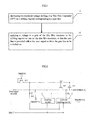
- the shifting register according to the embodiment includes three TFTs, a storage capacitor, a resetting module, a feedback receiving module, and corresponding I/O terminals.
- the shifting register includes:
- a first TFT M1 having a gate and a source connected together and further connected to a trigger signal terminal Input(n) at the present stage (i.e., at the n th stage), and a drain connected to a first node PU as a pull-up node, for controlling the shifting register to start operation upon receiving a high level signal sent from the trigger signal terminal Input(n), wherein the trigger signal terminal Input(n) receives a high level signal when an output terminal Output(n-1) of the shifting register at the previous stage (i.e., the shifting register at the (n-1) th stage) outputs a high level;
- a second thin film transistor M2 having a gate connected to the first node PU, a source connected to a clock signal terminal, and a drain connected to an output terminal Output(n) at the present stage, for providing a high level output for the output terminal Output(n) to drive the gate line corresponding to the shifting register at the present stage (i.e., the shifting register at the n th stage) to be switched on;
- a third TFT M3 having a gate connected to the first node PU, a source connected to the clock signal terminal, and a drain connected to a trigger signal terminal Input(n+1) for the next stage (i.e., the (n+1) th stage), for providing a trigger signal for the shifting register at the next stage(i.e., the shifting register at the (n+1) th stage) to control the same to start operation;
- a capacitor C1 being connected between the first node PU and the output terminal Output(n) at the present stage;
- a resetting module 1 being connected between a second node PL as a pull-down node, the clock signal terminal and a low level signal terminal Vss, for applying a low level to the drain and the gate of the second TFT M2 after the output of the present stage is completed;
- a feedback receiving module 2 being connected between the first node PU, the low level signal terminal Vss and the output terminal Output(n) at the present stage, and being further connected to the feedback signal terminal Reset(n+1), for receiving a feedback signal from the next stage to pull down the levels at the first node PU and the output terminal Output(n) at the present stage, wherein the feedback signal terminal Reset(n+1) receives a high level signal when the output terminal Output(n+1) of the shifting register at the next stage (i.e., the shifting register at the (n+1) th stage) outputs a high level; and the feedback signal terminal Reset(n+1) can be either connected to the output terminal Output(n+1) of the shifting register at the next stage (i.e., the shifting register at the (n+1) th stage), or connected to a trigger signal terminal Input(n+2) of the shifting register at the stage subsequent to the next stage of the present stage (i.e., the shifting register at the (n+2) th stage).
- the shifting register in Fig.2 includes three TFTs, the embodiments of the disclosure are not limited thereto.
- the third TFT M3 can be excluded, and the output terminal Output(n) at the present stage connected to the drain of the second TFT M2 can serve to be connected to the trigger signal terminal Input(n+1) for the next stage.
- a shifting register includes two TFTs, a storage capacitor, a resetting module, a feedback receiving module and corresponding I/O terminals.
- the shifting register includes:
- a first TFT M1 having a gate and a source connected together and further connected to a trigger signal terminal Input(n) at the present stage, and a drain connected to a first node PU as a pull-up node, for controlling the shifting register to start operation upon receiving a high level signal sent from the trigger signal terminal Input(n) at the present stage, wherein the trigger signal terminal Input(n) receives a high level signal when an output terminal Output(n-1) of the shifting register at the previous stage (i.e., the shifting register at the (n-1) th stage) outputs a high level;
- a second TFT M2 having a gate connected to the first node PU, a source connected to a clock signal terminal, and a drain connected to an output terminal Output(n) at the present stage and a trigger signal terminal Input(n+1) for the next stage, for providing a high level output for the output terminal Output(n) at the present stage so as to drive the gate line corresponding to the shifting register at the present stage (i.e., the shifting register at the n th stage) to be switched on, and to provide a trigger signal for the shifting register at the next stage (i.e., the shifting register at the (n+1) th stage) to control the same to start operation;
- a capacitor C1 being connected between the first node PU and the output terminal Output(n) at the present stage;
- a resetting module 1 being connected between a second node PL as a pull-down node, the clock signal terminal and a low level signal terminal Vss, for applying a low level to the drain and the gate of the second TFT M2 after the output of the present stage is completed;
- a feedback receiving module 2 being connected between the first node PU, the low level signal terminal Vss and the output terminal Output(n) at the present stage, and being further connected to a feedback signal terminal Reset(n+1), for receiving a feedback signal from the next stage to pull down the levels at the first node PU and the output terminal Output(n) of the present stage, wherein the feedback signal terminal Reset (n+1) receives a high level signal when the output terminal Output(n+1) of the shifting register at the next stage (i.e., the shifting register at the (n+1) th stage) outputs a high level; and the feedback signal terminal Reset(n+1) can be connected to the output terminal Output(n+1) of the shifting register at the next stage (i.e., the shifting register at the (n+1) th stage), or the feedback signal terminal Reset(n+1) can be connected to another TFT (e.g., the TFT M3 in Fig.2 ) which is added to the shifting register at the next stage (i.
- the shifting register provided in the embodiment of the disclosure, based on the principle of the tunnelling effect and the quantum mechanics, by applying a high level to the source of the TFT and a low level to the gate thereof, the electrons formed and accumulated on the gate insulation layer of the TFT can pass the potential barrier and arrive at the source thereof to decrease the threshold voltage shifting of the TFT in the shifting register corresponding to each gate line, and thus it allows the shifting register circuit to operate normally, improving the stability of the shifting register in operation and extending the lifespan of the shifting register.
- the threshold voltage shifting occurs in the individual TFTs in the shifting register due to the formation and accumulation of the electrons on the gate insulation layer of the corresponding TFTs, so the corresponding TFTs in the shifting register can be provided with a resetting module 1, for applying a high level to the source of the TFT and a low level to the gate thereof after the output of the present stage of the shifting register is completed, such that the electrons at the gate insulation layer of the TFT can arrive at the source thereof to decrease the threshold voltage shifting of the TFT.
- the second TFT M2 Since in the shifting register, the second TFT M2 can switch on the connection between the clock signal terminal and the output terminal of the present stage to allow the gate line corresponding to the shifting register to be switched on, the second TFT M2 plays a very important role in the shifting register. Once the second TFT M2 fails to be turned on normally due to the threshold voltage shifting, the quality of the display will be affected. In addition, the opeation current in the second TFT M2 is large in general, which tends to cause the threshold voltage shifting. Therefore, taking the second TFT M2 as an example in the embodiment, it describes how to decrease the threshold voltage shifting of the TFT by use of the resetting module 1. It should be appreciated that the description is only for illustration and not for limitation.
- the shifting register includes fourteen TFTs, a storage capacitor, and corresponding I/O terminals.
- the fourteen TFTs are as follows respectively: a first TFT M1, a second TFT M2, a third TFT M3, a fourth TFT M4, a fifth TFT M5, a sixth TFT M6, a seventh TFT M7, an eighth TFT M8, a ninth TFT M9, a tenth TFT M10, a first resetting TFT T1, a second resetting TFT T2, a third resetting TFT T3, and a fourth resetting TFT T4.
- the storage capacitor is shown as a capacitor C1.
- the I/O terminals includes: a trigger signal terminal Input(n) for receiving a trigger signal from the shifting register at the previous stage; an output terminal Output(n) for outputting a level signal for the shifting register at the present stage; a trigger signal terminal Input(n+1) for sending a trigger signal to the shifting register at the next stage; a feedback signal terminal Reset(n+1) for receiving a feedback signal from the shifting register at the next stage; a low level signal terminal Vss, and clock signal terminals, wherein the clock signal terminals include a first clock signal terminal CLK and a second clock signal terminal CLKB, and a clock signal at the first clock signal terminal CLK and that at the second clock signal terminal
- CLKB have the same frequency and duty cycle, but only differ in phase by 180°.
- the first TFT M1 has a gate and a source connected together and further connected to the trigger signal terminal Input(n) at the present stage, and a drain connected to a first node PU as a pull-up node;
- the second TFT M2 has a gate connected to the first node PU, a source connected to the first clock signal terminal CLK, and a drain connected to the output terminal Output(n) at the present stage;
- the third TFT M3 has a gate connected to the first node PU, a source connected to the first clock signal terminal CLK, and a drain connected to the trigger signal terminal Input(n+1) for the next stage;
- the fourth TFT M4 has a gate connected to the feedback signal terminal Reset(n+1), a source connected to the output terminal Output(n) at the present stage, and a drain connected to the low level signal terminal Vss;
- the fifth TFT M5 has a gate connected to the feedback signal terminal Reset(n+1), a source connected to the first node
- the first resetting TFT T1 has a gate connected to the second node PL, a source connected to a drain of the third resetting TFT M3, and a drain connected to the low level signal terminal Vss;
- the second resetting TFT T2 has a gate connected to the second node PL, a source connected to the drain of the fourth resetting TFT T4, and a drain connected to the low level signal terminal Vss;
- the third resetting TFT T3 has a gate and a source connected to the first clock signal terminal CLK, a drain connected to the source of the first resetting TFT T1;
- the fourth resetting TFT T4 has a gate connected to the drain of the third resetting TFT T3, a source connected to the first clock signal terminal CLK, and a drain connected to the source of the second resetting TFT T2.
- the storage capacitor is connected between the first node PU and the output terminal Output(n) at the present stage.
- the first resetting TFT T1, the second resetting TFT T2, the third resetting TFT T3 and the fourth resetting TFT T4 have the same structures as those of the first TFT M1 to the tenth TFT M10.
- the first resetting TFT T1, the second resetting TFT T2, the third resetting TFT T3 and the fourth resetting TFT T4 constitute the resetting module 1 of the present embodiment, and they are differentiated from the first TFT M1 to the tenth TFT M10 in the names.
- the first resetting TFT T1, the second resetting TFT T2, the third resetting TFT T3 and the fourth resetting TFT T4 constitute the resetting module 1 of the present embodiment, and the resetting module 1 is used for applying a high level to the source of the second TFT T2 and a low level to the gate thereof after the output of the present stage is completed, and thus according to the principle of the tunneling effect and the quantum mechanics, the electrons formed and accumulated at the gate insulation layer of the second TFT M2 can pass the potential barrier and arrive at the source of the second TFT M2 to decrease the threshold voltage shifting of the second TFT M2 in the shifting register corresponding to each of the gate lines, and finally it allows the shifting register circuit to operate normally, improving the stability of the shifting register in operation and extending the lifespan of the shifting register.
- the fourth TFT M4 and the fifth TFT M5 constitute the feedback receiving module 2.
- the feedback receiving module 2 keeps the output terminal Output(n) at the present stage and the first node PU as the pull-up node at a low level when the shifting register at the present stage is not in operation and the shifting register at the next stage is in operation, so as to avoid the occurrence of the following case: the output terminal Output(n) at the present stage changes to a high level under the influence of the other interference signals, and thus causes the gate line under the control thereof to be switched on, finally resulting in the switching-on of the gate line in error.
- the fourth TFT M4 keeps the output terminal Output(n) at the present stage at a low level under the action of the feedback signal terminal Reset(n+1), and the fifth TFT M5 keeps the first node PU at a low level under the action of the feedback signal terminal Reset(n+1), so as to prevent the second TFT M2 from turning on in error.
- the shifting register further includes the sixth TFT M6.
- the sixth TFT M6 when the shifting register at the present stage is not in operation, pulls down the second node PL as a pull-down node by receiving a high level signal at the second clock signal terminal CLKB, so as to avoid the occurrence of the following case: the output terminal Output(n) of the present stage changes to a high level under the influence of the other interference signals, and thus causes the gate line under the control thereof to be switched on, finally resulting in the switching-on of the gate line in error.
- the shifting register further includes the seventh TFT M7.
- the seventh TFT M7 accelerates the charging process of the storage capacitor C1 when the trigger signal terminal Input(n) at the present stage is at a high level and the second clock signal terminal CLKB changes to a high level.
- the shifting register further includes the eighth TFT M8.
- the eighth TFT M8 ensures the first node PU to be kept at a high level so as to continue to charge the capacitor C1 during the period in which the output terminal Output(n) at the present stage is at a high level (i.e., the period during which the shifting register at the present stage is in operation), further improving the turn-on capability of the second TFT M2.
- the shifting register further includes the ninth TFT M9 and the tenth TFT M10, and both TFTs are combined with the resetting module 1 so that both the gate and the drain of the second TFT M2 are at a low level upon the second TFT M2 is reset; wherein, the ninth TFT M9 pulls down the first node PU to be at a low level to prevent the second TFT M2 from turning on in error, and the tenth TFT M10 pulls down the output terminal Output(n) at the present stage to be at a low level to prevent the output terminal Output(n) from changing to a high level.
- the shifting register in Fig. 3 includes fourteen TFTs
- the embodiments of the disclosure are not limited thereto.
- a shifting register in accordance with another embodiment of the disclosure can exclude the third TFT M3, and the output terminal Output(n) at the present stage connected to the drain of the second TFT M2 can directly serve as the trigger signal terminal Input(n+1) for the next stage simultaneously.
- a shifting register includes thirteen TFTs, a storage capacitor, and corresponding I/O terminals.
- the thirteen TFTs are as follows respectively: a first TFT M1, a second TFT M2, a fourth TFT M4, a fifth TFT M5, a sixth TFT M6, a seventh TFT M7, an eighth TFT M8, a ninth TFT M9, a tenth TFT M10, a first resetting TFT T1, a second resetting TFT T2, a third resetting TFT T3, and a fourth resetting TFT T4.
- the storage capacitor is shown as a capacitor C1.
- the I/O terminals includes: a trigger signal terminal Input(n) for receiving the trigger signal from the shifting register at the previous stage; an output terminal Output(n) for outputting a level signal for the shifting register at the present stage and for sending a trigger signal to the shifting register at the next stage; a feedback signal terminal Reset(n+1) for receiving a feedback signal from the shifting register at the next stage; a low level signal terminal Vss, and clock signal terminals, wherein the clock signal terminals include a first clock signal terminal CLK and a second clock signal terminal CLKB, and a clock signal at the first clock signal terminal CLK and that at the second clock signal terminal CLKB have the same frequency and duty cycle, but only differ in phase by 180°.
- the operations on the thirteen TFTs are the same as those on the corresponding TFTs of the embodiment as described with reference to Fig. 3 , and the details are omitted.
- the TFTs in the embodiments of the disclosure can be of the type of hydrogenated amorphous TFTs, but can be of other types of TFTs.
- Fig. 4 it is the control timing chart for the shifting register in the embodiment, and there are four phases, i.e., t1, t2, t3 and t4 in the chart.
- the first clock signal terminal CLK and the second clock signal terminal CLKB alternate in use.
- STV denotes a switching signal terminal, i.e., the trigger signal terminal Input(n) at the present stage, for receiving a high level signal from the shifting register at the previous stage, wherein a high level signal is denoted by 1, and a low level signal is denoted by 0.
- an arrow " ⁇ " represents that the corresponding TFT is ON, and a cross "X" represents that the corresponding TFT is OFF.
- the signal at STV of the shifting register at the present stage is provided by the trigger signal terminal Input(n) at the present stage.
- the phase t1 is a phase during which the storage capacitor C1 is charged.
- the second TFT M2 turns on under the action of the storage capacitor C1, it outputs a high level at the first clock signal terminal CLK to the output terminal Output(n) at the present stage, and then the output terminal Output(n) at the present stage outputs the high level to the gate line corresponding to the shifting register at the present stage, turning on all the TFTs located in the row corresponding tothe gate line, and the data lines begin to write signals.
- the eighth TFT M8 turns on and feeds back the high level at the output terminal Output(n) to the first node PU, to ensure the first node PU to be kept at a high level to continue to charge the capacitor C1, further improving the turn-on capability of the second TFT M2.
- the third resetting TFT T3 turns on, and the first resetting TFT T1 can keep the gate of the fourth resetting TFT T4 at a low level by designing the width-to-length ratio of the channel of the first resetting TFT T1 and that of the third resetting TFT T3 appropriately.
- the second resetting TFT T2 keeps the drain of the fourth resetting TFT T4 at a low level.
- the ninth and tenth TFTs M9, M10 turn off, to ensure the first node PU and the output terminal Output(n) at the present stage at a high level continuously and not being pulled down.
- the third TFT M3 turns on, under the action of the storage capacitor C1, to allow the trigger signal terminal Input(n+1) for the next stage to change to a high level so as to send a trigger signal to the shifting register at the next stage.
- the phase t2 is the phase during which a high level is output to the output terminal Output(n) of the shifting register at the present stage.
- the Reset signal of the shifting register at the present stage is provided from the feedback signal terminal Reset(n+1).
- the sixth TFT M6 turns on, and it pulls the second node PL down to Vss when the shifting register at the present stage is not in operation, to prevent the output terminal Output(n) at the present stage from changing to a high level under the influence of the other interference signals.
- the phase t3 is the phase during which a high level is output to the output terminal Output(n+1) of the shifting register at the next stage.
- the third resetting TFT T3 turns on, which causes the gate of the fourth resetting TFT T4 to change to a high level, and thus the fourth resetting TFT T4 turns on.
- the gate of the ninth TFT M9 and that of the tenth TFT M10 change to a high level, and thus the ninth and the tenth TFTs M9, M10 turn on.
- the ninth TFT M9 pulls the first node PU down to Vss
- the tenth TFT M10 pulls the output terminal Output(n) down to Vss, so that both the gate and the drain of the second TFT M2 are at a low level when the second TFT M2 is reset.
- the electrons accumulated on the gate insulation layer of the second TFT M2 can pass the potential barrier to arrive at the source of the second TFT M2, and thus the threshold voltage shifting thereof is decreased.
- the phase t4 is the phase during which the resetting module 1 resets the second TFT M2, i.e., the resetting phase of the shifting register at the present stage.
- the shifting register in the embodiment can decrease the threshold voltage shifting of the TFTs in the shifting register corresponding to each of the gate lines, and finally it enables the shifting register circuit to operate normally, improving the stability of the shifting register in operation and extending the lifespan of the shifting register.
- the above operation process can be also applied to the embodiment in which the third TFT M3 is excluded, and the details are omitted.
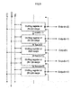
- the gate line driving apparatus includes a plurality of shifting registers connected in series, and for the sake of simplicity, it is only shown five shifting registers in Fig. 9 , i.e., the (N-2) th shifting register, the (N-1) th shifting register, the N th shifting register, the (N+1) th shifting register, and the (N+2) th shifting register, respectively.
- the output terminal Output(n) of the N th shifting register not only feeds back a feedback signal to the (N-1) th shifting register to switch off the (N-1) th shifting register, but also outputs a trigger signal to the (N+1) th shifting register for triggering the (N+1) th shifting register.
- the clock signal CLK and the clock signal CLKB alternate in use.
- the clock signal terminal of the N th shifting register receives the clock signal CLK
- the clock signal terminals of the (N-1) th and (N+1) th shifting registers receive the clock signal CLKB. Therefore, the clock signal for the N th shifting register and those for the (N-1) th and (N+1) th shifting registers have totally inverted phases, that is, differ in phase by 180°.
- the clock signal terminals includes a first clock signal terminal and a second clock signal terminal
- the clock signal CLK and the clock signal CLKB also alternate in use.
- For the N th shifting register its first clock signal terminal receives the clock signal CLK and its second clock signal terminal receives the clock signal CLKB
- their first clock signal terminal receives the clock signal CLKB
- their second clock signal terminal receives the clock signal CLK.
- the shifting register at each stage includes three TFTs, a storage capacitor, a resetting module, a feedback receiving module, and corresponding I/O terminals.
- the shifting register includes:
- a first TFT M1 having a gate and a source connected together and further connected to the trigger signal terminal Input(n) at the present stage, and a drain connected to a first node PU as a pull-up node, for controlling the shifting register to start operation upon receiving a high level signal sent from the trigger signal terminal Input(n), wherein the trigger signal terminal Input(n) receives a high level signal when an output terminal Output(n-1) of the shifting register at the previous stage (i.e., the shifting register at the (n-1) th stage) outputs a high level; a second thin film transistor M2, having a gate connected to the first node PU, a source connected to a clock signal terminal, and a drain connected to the output terminal Output(n) at the present stage, for providing a high level to the output terminal Output(n) to drive a gate line corresponding to the shifting register at the present stage (i.e., the shifting register at the n th stage) to be switched on; a third TFT
- the output terminal Output(n) of the N th shifting register feeds back a feedback signal to the (N-1) th shifting register (that is, serves as the feedback signal terminal Reset(n-1) at the previous stage) to switch off the (N-1) th shifting register, and at the same time, the trigger signal terminal Input(n+1) of the shifting register at the N th stage outputs a signal to the (N+1) th shifting register, which serves as a trigger signal for the (N+1) th shifting register.
- the shifting register at each stage in the gate line driving apparatus in accordance with the another embodiment of the disclosure excludes the third TFT M3, and the output terminal Output(n) at the present stage connected to the drain of the second TFT M2 can directly serve as a trigger signal terminal Input(n+1) for the next stage simultaneously.
- the operation on the shifting register is the same as that of the shifting register in the gate line driving apparatus in the embodiment of the disclosure, and the details are omitted.
- the gate line driving apparatus by applying a high level to the source of the TFT and a low level to the gate thereof, according to the principle of the tunneling effect and the quantum mechanics, the electrons formed and accumulated on the gate insulation layer of the TFT can pass the potential barrier and arrive at the source of the TFT, and thus it decreases the threshold voltage shifting of the TFT in the shifting register corresponding to each gate line, and finally it enables the shifting register circuit to operate normally, improving the stability of the shifting register in operation and extending the lifespan of the shifting register.
- the shifting register used in the gate line driving apparatus has the same function and structure as those of the shifting register used in the embodiments for the shifting register, and thus that they can solve the same technical problem, achieve the same expected effect.
- the disclosure also provides a display device comprising a pixel array and the gate line driving apparatus as described above.
Landscapes
- Engineering & Computer Science (AREA)
- Chemical & Material Sciences (AREA)
- Crystallography & Structural Chemistry (AREA)
- Physics & Mathematics (AREA)
- Computer Hardware Design (AREA)
- General Physics & Mathematics (AREA)
- Theoretical Computer Science (AREA)
- Control Of Indicators Other Than Cathode Ray Tubes (AREA)
- Shift Register Type Memory (AREA)
- Liquid Crystal Display Device Control (AREA)
Applications Claiming Priority (2)
| Application Number | Priority Date | Filing Date | Title |
|---|---|---|---|
| CN201110331772XA CN102629459A (zh) | 2011-10-26 | 2011-10-26 | 栅线驱动方法、移位寄存器及栅线驱动装置 |
| PCT/CN2012/083558 WO2013060285A1 (zh) | 2011-10-26 | 2012-10-26 | 栅线驱动方法、移位寄存器、栅线驱动装置及显示设备 |
Publications (3)
| Publication Number | Publication Date |
|---|---|
| EP2772902A1 true EP2772902A1 (de) | 2014-09-03 |
| EP2772902A4 EP2772902A4 (de) | 2015-04-01 |
| EP2772902B1 EP2772902B1 (de) | 2019-03-20 |
Family
ID=46587711
Family Applications (1)
| Application Number | Title | Priority Date | Filing Date |
|---|---|---|---|
| EP12790780.6A Not-in-force EP2772902B1 (de) | 2011-10-26 | 2012-10-26 | Ansteuerverfahren und ansteuervorrichtung fur gate leitungen, shieberegister und anzeigevorrichtung |
Country Status (6)
| Country | Link |
|---|---|
| US (1) | US20140050294A1 (de) |
| EP (1) | EP2772902B1 (de) |
| JP (2) | JP2015502564A (de) |
| KR (1) | KR101459521B1 (de) |
| CN (1) | CN102629459A (de) |
| WO (1) | WO2013060285A1 (de) |
Cited By (1)
| Publication number | Priority date | Publication date | Assignee | Title |
|---|---|---|---|---|
| CN113056783A (zh) * | 2019-10-28 | 2021-06-29 | 京东方科技集团股份有限公司 | 移位寄存器单元及其驱动方法、栅极驱动电路和显示装置 |
Families Citing this family (29)
| Publication number | Priority date | Publication date | Assignee | Title |
|---|---|---|---|---|
| CN102629459A (zh) * | 2011-10-26 | 2012-08-08 | 北京京东方光电科技有限公司 | 栅线驱动方法、移位寄存器及栅线驱动装置 |
| CN102682689B (zh) * | 2012-04-13 | 2014-11-26 | 京东方科技集团股份有限公司 | 一种移位寄存器、栅极驱动电路及显示装置 |
| CN102867475A (zh) * | 2012-09-13 | 2013-01-09 | 京东方科技集团股份有限公司 | 移位寄存器单元、栅极驱动电路及显示装置 |
| CN102915714B (zh) * | 2012-10-11 | 2015-05-27 | 京东方科技集团股份有限公司 | 一种移位寄存器、液晶显示栅极驱动装置和液晶显示装置 |
| TWI500265B (zh) * | 2012-11-22 | 2015-09-11 | Au Optronics Corp | 移位暫存器 |
| CN103021466B (zh) * | 2012-12-14 | 2016-08-03 | 京东方科技集团股份有限公司 | 移位寄存器及其工作方法、栅极驱动装置、显示装置 |
| CN103021318B (zh) | 2012-12-14 | 2016-02-17 | 京东方科技集团股份有限公司 | 移位寄存器及其工作方法、栅极驱动装置、显示装置 |
| CN103700355B (zh) * | 2013-12-20 | 2016-05-04 | 京东方科技集团股份有限公司 | 一种移位寄存器单元、栅极驱动电路及显示器件 |
| CN103985341B (zh) * | 2014-04-30 | 2016-04-20 | 京东方科技集团股份有限公司 | 一种移位寄存器单元、栅极驱动电路和显示装置 |
| KR102367484B1 (ko) * | 2014-09-30 | 2022-02-28 | 엘지디스플레이 주식회사 | 표시장치 및 이의 구동방법 |
| CN106575494B (zh) | 2014-07-31 | 2019-11-05 | 乐金显示有限公司 | 显示装置 |
| CN104200769B (zh) * | 2014-08-19 | 2016-09-28 | 上海和辉光电有限公司 | 扫描信号产生电路 |
| CN104409056B (zh) * | 2014-11-14 | 2017-01-11 | 深圳市华星光电技术有限公司 | 一种扫描驱动电路 |
| CN104392705B (zh) * | 2014-12-15 | 2016-09-21 | 京东方科技集团股份有限公司 | 移位寄存器、栅极驱动电路、阵列基板、显示装置 |
| CN104700769B (zh) * | 2015-04-09 | 2017-03-15 | 京东方科技集团股份有限公司 | 移位寄存器单元、栅极驱动装置以及显示装置 |
| CN108665854A (zh) * | 2017-03-27 | 2018-10-16 | 昆山工研院新型平板显示技术中心有限公司 | 控制信号驱动电路与驱动方法以及像素电路驱动方法 |
| CN108172180B (zh) * | 2017-12-18 | 2020-06-05 | 深圳市华星光电技术有限公司 | 一种液晶显示器的驱动装置及其复位的方法 |
| CN108024149B (zh) * | 2017-12-18 | 2020-09-04 | 海信视像科技股份有限公司 | TCON板通过单条连接线向SoC芯片传输信号的方法、TCON板及电视机 |
| CN107978294A (zh) * | 2018-01-12 | 2018-05-01 | 京东方科技集团股份有限公司 | 移位寄存器单元、移位寄存器电路、显示面板 |
| CN110322848B (zh) | 2018-03-30 | 2021-01-08 | 京东方科技集团股份有限公司 | 移位寄存器单元、栅极驱动电路、显示装置及驱动方法 |
| KR102442099B1 (ko) * | 2018-05-31 | 2022-09-13 | 에스케이하이닉스 주식회사 | 다중-입력 쉬프트 레지스터(misr) 회로를 구비한 반도체 장치 |
| WO2020073231A1 (zh) * | 2018-10-10 | 2020-04-16 | 深圳市柔宇科技有限公司 | 一种goa电路及显示装置 |
| CN109509443A (zh) * | 2018-12-04 | 2019-03-22 | 昆山龙腾光电有限公司 | 栅极驱动电路及显示装置 |
| CN109285496B (zh) * | 2018-12-07 | 2021-11-12 | 合肥鑫晟光电科技有限公司 | 移位寄存器单元、栅极驱动电路及其驱动方法、显示装置 |
| CN109346008A (zh) * | 2018-12-17 | 2019-02-15 | 武汉华星光电半导体显示技术有限公司 | 有机发光二极管显示装置 |
| CN109410885A (zh) * | 2018-12-27 | 2019-03-01 | 信利半导体有限公司 | 扫描驱动电路、像素阵列基板及显示面板 |
| CN109799870B (zh) * | 2018-12-29 | 2021-03-05 | 深圳云天励飞技术有限公司 | 一种时钟控制电路及控制方法 |
| CN110517624B (zh) * | 2019-09-27 | 2022-10-04 | 合肥京东方显示技术有限公司 | 移位寄存器单元、栅极驱动电路和显示装置 |
| CN110867157A (zh) * | 2019-11-29 | 2020-03-06 | 昆山国显光电有限公司 | 显示面板及像素驱动方法 |
Family Cites Families (40)
| Publication number | Priority date | Publication date | Assignee | Title |
|---|---|---|---|---|
| KR100797522B1 (ko) * | 2002-09-05 | 2008-01-24 | 삼성전자주식회사 | 쉬프트 레지스터와 이를 구비하는 액정 표시 장치 |
| KR100917009B1 (ko) * | 2003-02-10 | 2009-09-10 | 삼성전자주식회사 | 트랜지스터의 구동 방법과 쉬프트 레지스터의 구동 방법및 이를 수행하기 위한 쉬프트 레지스터 |
| KR100551729B1 (ko) * | 2003-03-19 | 2006-02-13 | 비오이 하이디스 테크놀로지 주식회사 | 액정표시장치의 게이트 라인 구동방법 및 그 구동회로 |
| KR20060123913A (ko) * | 2005-05-30 | 2006-12-05 | 삼성전자주식회사 | 쉬프트 레지스터 및 이를 갖는 표시장치 |
| KR20070013013A (ko) * | 2005-07-25 | 2007-01-30 | 삼성전자주식회사 | 표시 장치 |
| US8174478B2 (en) * | 2006-06-12 | 2012-05-08 | Samsung Electronics Co., Ltd. | Gate driving circuit and display apparatus having the same |
| KR101182770B1 (ko) * | 2006-06-12 | 2012-09-14 | 삼성디스플레이 주식회사 | 게이트 구동회로 및 이를 갖는 표시장치 |
| KR101217177B1 (ko) * | 2006-06-21 | 2012-12-31 | 삼성디스플레이 주식회사 | 게이트 구동회로 및 이를 갖는 표시 장치 |
| US7936332B2 (en) * | 2006-06-21 | 2011-05-03 | Samsung Electronics Co., Ltd. | Gate driving circuit having reduced ripple effect and display apparatus having the same |
| TWI349906B (en) * | 2006-09-01 | 2011-10-01 | Au Optronics Corp | Shift register, shift register array circuit, and display apparatus |
| JP5079301B2 (ja) * | 2006-10-26 | 2012-11-21 | 三菱電機株式会社 | シフトレジスタ回路およびそれを備える画像表示装置 |
| TWI385624B (zh) * | 2007-04-11 | 2013-02-11 | Wintek Corp | 移位暫存器及其位準控制器 |
| KR101617215B1 (ko) * | 2007-07-06 | 2016-05-03 | 삼성디스플레이 주식회사 | 액정 표시 장치 및 그의 구동 방법 |
| KR101415562B1 (ko) * | 2007-08-06 | 2014-07-07 | 삼성디스플레이 주식회사 | 게이트 구동회로 및 이를 가지는 표시장치 |
| CN101546607B (zh) * | 2008-03-26 | 2012-02-29 | 北京京东方光电科技有限公司 | 移位寄存器及液晶显示器栅极驱动装置 |
| KR101472513B1 (ko) * | 2008-07-08 | 2014-12-16 | 삼성디스플레이 주식회사 | 게이트 드라이버 및 이를 갖는 표시장치 |
| KR101502361B1 (ko) * | 2008-08-06 | 2015-03-16 | 삼성디스플레이 주식회사 | 액정 표시 장치 |
| KR101471553B1 (ko) * | 2008-08-14 | 2014-12-10 | 삼성디스플레이 주식회사 | 게이트 구동 회로 및 이를 갖는 표시 장치 |
| CN101677021B (zh) * | 2008-09-19 | 2013-07-17 | 北京京东方光电科技有限公司 | 移位寄存器的级、栅线驱动器、阵列基板和液晶显示装置 |
| KR101579842B1 (ko) * | 2008-10-30 | 2015-12-24 | 삼성디스플레이 주식회사 | 게이트 라인 구동 방법, 이를 수행하기 위한 게이트 구동회로 및 이를 구비한 표시 장치 |
| JP5318117B2 (ja) * | 2008-12-10 | 2013-10-16 | シャープ株式会社 | 走査信号線駆動回路、シフトレジスタ、およびシフトレジスタの駆動方法 |
| KR101579082B1 (ko) * | 2008-12-23 | 2015-12-22 | 삼성디스플레이 주식회사 | 게이트 구동회로 및 이의 구동 방법 |
| KR101520807B1 (ko) * | 2009-01-05 | 2015-05-18 | 삼성디스플레이 주식회사 | 게이트 구동회로 및 이를 갖는 표시장치 |
| TWI402814B (zh) * | 2009-01-16 | 2013-07-21 | Chunghwa Picture Tubes Ltd | 可抑制臨界電壓漂移之閘極驅動電路 |
| KR101543281B1 (ko) * | 2009-02-19 | 2015-08-11 | 삼성디스플레이 주식회사 | 게이트 구동회로 및 이를 구비한 표시 장치 |
| CN101847445B (zh) * | 2009-03-27 | 2012-11-21 | 北京京东方光电科技有限公司 | 移位寄存器及其栅线驱动装置 |
| KR101573460B1 (ko) * | 2009-04-30 | 2015-12-02 | 삼성디스플레이 주식회사 | 게이트 구동회로 |
| CN102012591B (zh) * | 2009-09-04 | 2012-05-30 | 北京京东方光电科技有限公司 | 移位寄存器单元及液晶显示器栅极驱动装置 |
| KR101587610B1 (ko) * | 2009-09-21 | 2016-01-25 | 삼성디스플레이 주식회사 | 구동회로 |
| KR101605433B1 (ko) * | 2009-11-26 | 2016-03-23 | 삼성디스플레이 주식회사 | 표시 패널 |
| WO2011092924A1 (ja) * | 2010-01-29 | 2011-08-04 | シャープ株式会社 | シフトレジスタおよび表示装置 |
| KR101641721B1 (ko) * | 2010-06-24 | 2016-07-25 | 삼성디스플레이 주식회사 | 표시장치의 구동회로 |
| TWI409528B (zh) * | 2010-07-02 | 2013-09-21 | Chunghwa Picture Tubes Ltd | 顯示面板 |
| CN102467890B (zh) * | 2010-10-29 | 2014-05-07 | 京东方科技集团股份有限公司 | 移位寄存器单元、栅极驱动装置及液晶显示器 |
| KR101810517B1 (ko) * | 2011-05-18 | 2017-12-20 | 삼성디스플레이 주식회사 | 게이트 구동회로 및 이를 구비한 표시 장치 |
| CN102629459A (zh) * | 2011-10-26 | 2012-08-08 | 北京京东方光电科技有限公司 | 栅线驱动方法、移位寄存器及栅线驱动装置 |
| CN102654986A (zh) * | 2011-11-25 | 2012-09-05 | 京东方科技集团股份有限公司 | 移位寄存器的级、栅极驱动器、阵列基板以及显示装置 |
| CN102708779B (zh) * | 2012-01-13 | 2014-05-14 | 京东方科技集团股份有限公司 | 移位寄存器及其驱动方法、栅极驱动装置与显示装置 |
| CN102708926B (zh) * | 2012-05-21 | 2015-09-16 | 京东方科技集团股份有限公司 | 一种移位寄存器单元、移位寄存器、显示装置和驱动方法 |
| CN102945657B (zh) * | 2012-10-29 | 2014-09-10 | 京东方科技集团股份有限公司 | 移位寄存器单元、栅极驱动电路、阵列基板和显示装置 |
-
2011
- 2011-10-26 CN CN201110331772XA patent/CN102629459A/zh active Pending
-
2012
- 2012-10-26 WO PCT/CN2012/083558 patent/WO2013060285A1/zh not_active Ceased
- 2012-10-26 US US13/805,414 patent/US20140050294A1/en not_active Abandoned
- 2012-10-26 KR KR1020127032628A patent/KR101459521B1/ko active Active
- 2012-10-26 EP EP12790780.6A patent/EP2772902B1/de not_active Not-in-force
- 2012-10-26 JP JP2014537480A patent/JP2015502564A/ja active Pending
-
2017
- 2017-08-08 JP JP2017153610A patent/JP6501837B2/ja not_active Expired - Fee Related
Cited By (2)
| Publication number | Priority date | Publication date | Assignee | Title |
|---|---|---|---|---|
| CN113056783A (zh) * | 2019-10-28 | 2021-06-29 | 京东方科技集团股份有限公司 | 移位寄存器单元及其驱动方法、栅极驱动电路和显示装置 |
| CN113056783B (zh) * | 2019-10-28 | 2022-12-13 | 京东方科技集团股份有限公司 | 移位寄存器单元及其驱动方法、栅极驱动电路和显示装置 |
Also Published As
| Publication number | Publication date |
|---|---|
| KR101459521B1 (ko) | 2014-11-07 |
| EP2772902A4 (de) | 2015-04-01 |
| KR20130056876A (ko) | 2013-05-30 |
| JP2015502564A (ja) | 2015-01-22 |
| WO2013060285A1 (zh) | 2013-05-02 |
| JP6501837B2 (ja) | 2019-04-17 |
| JP2017204006A (ja) | 2017-11-16 |
| CN102629459A (zh) | 2012-08-08 |
| EP2772902B1 (de) | 2019-03-20 |
| US20140050294A1 (en) | 2014-02-20 |
Similar Documents
| Publication | Publication Date | Title |
|---|---|---|
| EP2772902B1 (de) | Ansteuerverfahren und ansteuervorrichtung fur gate leitungen, shieberegister und anzeigevorrichtung | |
| EP2838079B1 (de) | Schieberegistereinheit und ansteuerungsverfahren dafür, schieberegister und anzeigevorrichtung | |
| JP5473686B2 (ja) | 走査線駆動回路 | |
| US8615066B2 (en) | Shift register circuit | |
| JP5436335B2 (ja) | 走査線駆動回路 | |
| US12230213B2 (en) | Gate driver and organic light emitting display device including the same | |
| JP5419762B2 (ja) | シフトレジスタ回路 | |
| US9620061B2 (en) | Gate driver circuit, gate driving method, gate-on-array circuit, display device, and electronic product | |
| US11183114B2 (en) | Display panel, compensation method thereof and display device compensating an organic light-emitting element | |
| US9536476B2 (en) | Gate driver circuit, gate driving method, gate-on-array circuit, display device, and electronic product | |
| CN109801594B (zh) | 一种显示面板和显示装置 | |
| KR20130003252A (ko) | 스테이지 회로 및 이를 이용한 주사 구동부 | |
| US11289026B2 (en) | Pixel circuit, driving method thereof, display substrate and display device | |
| WO2010116778A1 (ja) | シフトレジスタおよびそれを備えた表示装置、ならびにシフトレジスタの駆動方法 | |
| KR20190090850A (ko) | Goa회로, 어레이 기판 및 디스플레이 장치 | |
| US20060132182A1 (en) | Driver circuit, shift register, and liquid crystal driver circuit | |
| KR101768541B1 (ko) | 쉬프트 레지스터 | |
| US10127877B2 (en) | Display device | |
| KR20250119927A (ko) | 표시장치 및 구동방법 | |
| KR20130016496A (ko) | 유기전계발광표시장치 |
Legal Events
| Date | Code | Title | Description |
|---|---|---|---|
| PUAI | Public reference made under article 153(3) epc to a published international application that has entered the european phase |
Free format text: ORIGINAL CODE: 0009012 |
|
| 17P | Request for examination filed |
Effective date: 20121203 |
|
| AK | Designated contracting states |
Kind code of ref document: A1 Designated state(s): AL AT BE BG CH CY CZ DE DK EE ES FI FR GB GR HR HU IE IS IT LI LT LU LV MC MK MT NL NO PL PT RO RS SE SI SK SM TR |
|
| DAX | Request for extension of the european patent (deleted) | ||
| RA4 | Supplementary search report drawn up and despatched (corrected) |
Effective date: 20150304 |
|
| RIC1 | Information provided on ipc code assigned before grant |
Ipc: G11C 19/18 20060101AFI20150226BHEP Ipc: G09G 3/36 20060101ALN20150226BHEP |
|
| 17Q | First examination report despatched |
Effective date: 20151221 |
|
| STAA | Information on the status of an ep patent application or granted ep patent |
Free format text: STATUS: EXAMINATION IS IN PROGRESS |
|
| REG | Reference to a national code |
Ref country code: DE Ref legal event code: R079 Ref document number: 602012058068 Country of ref document: DE Free format text: PREVIOUS MAIN CLASS: G09G0003360000 Ipc: G11C0019180000 |
|
| GRAP | Despatch of communication of intention to grant a patent |
Free format text: ORIGINAL CODE: EPIDOSNIGR1 |
|
| STAA | Information on the status of an ep patent application or granted ep patent |
Free format text: STATUS: GRANT OF PATENT IS INTENDED |
|
| RIC1 | Information provided on ipc code assigned before grant |
Ipc: G11C 19/18 20060101AFI20180913BHEP Ipc: G09G 3/36 20060101ALN20180913BHEP |
|
| INTG | Intention to grant announced |
Effective date: 20180925 |
|
| RIC1 | Information provided on ipc code assigned before grant |
Ipc: G11C 19/18 20060101AFI20180917BHEP Ipc: G09G 3/36 20060101ALN20180917BHEP |
|
| GRAS | Grant fee paid |
Free format text: ORIGINAL CODE: EPIDOSNIGR3 |
|
| GRAA | (expected) grant |
Free format text: ORIGINAL CODE: 0009210 |
|
| STAA | Information on the status of an ep patent application or granted ep patent |
Free format text: STATUS: THE PATENT HAS BEEN GRANTED |
|
| AK | Designated contracting states |
Kind code of ref document: B1 Designated state(s): AL AT BE BG CH CY CZ DE DK EE ES FI FR GB GR HR HU IE IS IT LI LT LU LV MC MK MT NL NO PL PT RO RS SE SI SK SM TR |
|
| REG | Reference to a national code |
Ref country code: GB Ref legal event code: FG4D |
|
| REG | Reference to a national code |
Ref country code: CH Ref legal event code: EP |
|
| REG | Reference to a national code |
Ref country code: DE Ref legal event code: R096 Ref document number: 602012058068 Country of ref document: DE |
|
| REG | Reference to a national code |
Ref country code: AT Ref legal event code: REF Ref document number: 1111325 Country of ref document: AT Kind code of ref document: T Effective date: 20190415 |
|
| REG | Reference to a national code |
Ref country code: IE Ref legal event code: FG4D |
|
| REG | Reference to a national code |
Ref country code: NL Ref legal event code: FP |
|
| PG25 | Lapsed in a contracting state [announced via postgrant information from national office to epo] |
Ref country code: SE Free format text: LAPSE BECAUSE OF FAILURE TO SUBMIT A TRANSLATION OF THE DESCRIPTION OR TO PAY THE FEE WITHIN THE PRESCRIBED TIME-LIMIT Effective date: 20190320 Ref country code: NO Free format text: LAPSE BECAUSE OF FAILURE TO SUBMIT A TRANSLATION OF THE DESCRIPTION OR TO PAY THE FEE WITHIN THE PRESCRIBED TIME-LIMIT Effective date: 20190620 Ref country code: FI Free format text: LAPSE BECAUSE OF FAILURE TO SUBMIT A TRANSLATION OF THE DESCRIPTION OR TO PAY THE FEE WITHIN THE PRESCRIBED TIME-LIMIT Effective date: 20190320 Ref country code: LT Free format text: LAPSE BECAUSE OF FAILURE TO SUBMIT A TRANSLATION OF THE DESCRIPTION OR TO PAY THE FEE WITHIN THE PRESCRIBED TIME-LIMIT Effective date: 20190320 |
|
| REG | Reference to a national code |
Ref country code: LT Ref legal event code: MG4D |
|
| PG25 | Lapsed in a contracting state [announced via postgrant information from national office to epo] |
Ref country code: BG Free format text: LAPSE BECAUSE OF FAILURE TO SUBMIT A TRANSLATION OF THE DESCRIPTION OR TO PAY THE FEE WITHIN THE PRESCRIBED TIME-LIMIT Effective date: 20190620 Ref country code: GR Free format text: LAPSE BECAUSE OF FAILURE TO SUBMIT A TRANSLATION OF THE DESCRIPTION OR TO PAY THE FEE WITHIN THE PRESCRIBED TIME-LIMIT Effective date: 20190621 Ref country code: RS Free format text: LAPSE BECAUSE OF FAILURE TO SUBMIT A TRANSLATION OF THE DESCRIPTION OR TO PAY THE FEE WITHIN THE PRESCRIBED TIME-LIMIT Effective date: 20190320 Ref country code: HR Free format text: LAPSE BECAUSE OF FAILURE TO SUBMIT A TRANSLATION OF THE DESCRIPTION OR TO PAY THE FEE WITHIN THE PRESCRIBED TIME-LIMIT Effective date: 20190320 Ref country code: LV Free format text: LAPSE BECAUSE OF FAILURE TO SUBMIT A TRANSLATION OF THE DESCRIPTION OR TO PAY THE FEE WITHIN THE PRESCRIBED TIME-LIMIT Effective date: 20190320 |
|
| REG | Reference to a national code |
Ref country code: AT Ref legal event code: MK05 Ref document number: 1111325 Country of ref document: AT Kind code of ref document: T Effective date: 20190320 |
|
| PG25 | Lapsed in a contracting state [announced via postgrant information from national office to epo] |
Ref country code: IT Free format text: LAPSE BECAUSE OF FAILURE TO SUBMIT A TRANSLATION OF THE DESCRIPTION OR TO PAY THE FEE WITHIN THE PRESCRIBED TIME-LIMIT Effective date: 20190320 Ref country code: RO Free format text: LAPSE BECAUSE OF FAILURE TO SUBMIT A TRANSLATION OF THE DESCRIPTION OR TO PAY THE FEE WITHIN THE PRESCRIBED TIME-LIMIT Effective date: 20190320 Ref country code: CZ Free format text: LAPSE BECAUSE OF FAILURE TO SUBMIT A TRANSLATION OF THE DESCRIPTION OR TO PAY THE FEE WITHIN THE PRESCRIBED TIME-LIMIT Effective date: 20190320 Ref country code: SK Free format text: LAPSE BECAUSE OF FAILURE TO SUBMIT A TRANSLATION OF THE DESCRIPTION OR TO PAY THE FEE WITHIN THE PRESCRIBED TIME-LIMIT Effective date: 20190320 Ref country code: EE Free format text: LAPSE BECAUSE OF FAILURE TO SUBMIT A TRANSLATION OF THE DESCRIPTION OR TO PAY THE FEE WITHIN THE PRESCRIBED TIME-LIMIT Effective date: 20190320 Ref country code: AL Free format text: LAPSE BECAUSE OF FAILURE TO SUBMIT A TRANSLATION OF THE DESCRIPTION OR TO PAY THE FEE WITHIN THE PRESCRIBED TIME-LIMIT Effective date: 20190320 Ref country code: PT Free format text: LAPSE BECAUSE OF FAILURE TO SUBMIT A TRANSLATION OF THE DESCRIPTION OR TO PAY THE FEE WITHIN THE PRESCRIBED TIME-LIMIT Effective date: 20190720 Ref country code: ES Free format text: LAPSE BECAUSE OF FAILURE TO SUBMIT A TRANSLATION OF THE DESCRIPTION OR TO PAY THE FEE WITHIN THE PRESCRIBED TIME-LIMIT Effective date: 20190320 |
|
| PG25 | Lapsed in a contracting state [announced via postgrant information from national office to epo] |
Ref country code: SM Free format text: LAPSE BECAUSE OF FAILURE TO SUBMIT A TRANSLATION OF THE DESCRIPTION OR TO PAY THE FEE WITHIN THE PRESCRIBED TIME-LIMIT Effective date: 20190320 Ref country code: PL Free format text: LAPSE BECAUSE OF FAILURE TO SUBMIT A TRANSLATION OF THE DESCRIPTION OR TO PAY THE FEE WITHIN THE PRESCRIBED TIME-LIMIT Effective date: 20190320 |
|
| PG25 | Lapsed in a contracting state [announced via postgrant information from national office to epo] |
Ref country code: AT Free format text: LAPSE BECAUSE OF FAILURE TO SUBMIT A TRANSLATION OF THE DESCRIPTION OR TO PAY THE FEE WITHIN THE PRESCRIBED TIME-LIMIT Effective date: 20190320 Ref country code: IS Free format text: LAPSE BECAUSE OF FAILURE TO SUBMIT A TRANSLATION OF THE DESCRIPTION OR TO PAY THE FEE WITHIN THE PRESCRIBED TIME-LIMIT Effective date: 20190720 |
|
| REG | Reference to a national code |
Ref country code: DE Ref legal event code: R097 Ref document number: 602012058068 Country of ref document: DE |
|
| PLBE | No opposition filed within time limit |
Free format text: ORIGINAL CODE: 0009261 |
|
| STAA | Information on the status of an ep patent application or granted ep patent |
Free format text: STATUS: NO OPPOSITION FILED WITHIN TIME LIMIT |
|
| PG25 | Lapsed in a contracting state [announced via postgrant information from national office to epo] |
Ref country code: DK Free format text: LAPSE BECAUSE OF FAILURE TO SUBMIT A TRANSLATION OF THE DESCRIPTION OR TO PAY THE FEE WITHIN THE PRESCRIBED TIME-LIMIT Effective date: 20190320 |
|
| 26N | No opposition filed |
Effective date: 20200102 |
|
| PG25 | Lapsed in a contracting state [announced via postgrant information from national office to epo] |
Ref country code: SI Free format text: LAPSE BECAUSE OF FAILURE TO SUBMIT A TRANSLATION OF THE DESCRIPTION OR TO PAY THE FEE WITHIN THE PRESCRIBED TIME-LIMIT Effective date: 20190320 |
|
| PG25 | Lapsed in a contracting state [announced via postgrant information from national office to epo] |
Ref country code: TR Free format text: LAPSE BECAUSE OF FAILURE TO SUBMIT A TRANSLATION OF THE DESCRIPTION OR TO PAY THE FEE WITHIN THE PRESCRIBED TIME-LIMIT Effective date: 20190320 |
|
| PG25 | Lapsed in a contracting state [announced via postgrant information from national office to epo] |
Ref country code: MC Free format text: LAPSE BECAUSE OF FAILURE TO SUBMIT A TRANSLATION OF THE DESCRIPTION OR TO PAY THE FEE WITHIN THE PRESCRIBED TIME-LIMIT Effective date: 20190320 |
|
| REG | Reference to a national code |
Ref country code: CH Ref legal event code: PL |
|
| PG25 | Lapsed in a contracting state [announced via postgrant information from national office to epo] |
Ref country code: LI Free format text: LAPSE BECAUSE OF NON-PAYMENT OF DUE FEES Effective date: 20191031 Ref country code: CH Free format text: LAPSE BECAUSE OF NON-PAYMENT OF DUE FEES Effective date: 20191031 Ref country code: LU Free format text: LAPSE BECAUSE OF NON-PAYMENT OF DUE FEES Effective date: 20191026 |
|
| REG | Reference to a national code |
Ref country code: BE Ref legal event code: MM Effective date: 20191031 |
|
| PG25 | Lapsed in a contracting state [announced via postgrant information from national office to epo] |
Ref country code: BE Free format text: LAPSE BECAUSE OF NON-PAYMENT OF DUE FEES Effective date: 20191031 |
|
| PG25 | Lapsed in a contracting state [announced via postgrant information from national office to epo] |
Ref country code: IE Free format text: LAPSE BECAUSE OF NON-PAYMENT OF DUE FEES Effective date: 20191026 |
|
| PG25 | Lapsed in a contracting state [announced via postgrant information from national office to epo] |
Ref country code: CY Free format text: LAPSE BECAUSE OF FAILURE TO SUBMIT A TRANSLATION OF THE DESCRIPTION OR TO PAY THE FEE WITHIN THE PRESCRIBED TIME-LIMIT Effective date: 20190320 |
|
| PG25 | Lapsed in a contracting state [announced via postgrant information from national office to epo] |
Ref country code: MT Free format text: LAPSE BECAUSE OF FAILURE TO SUBMIT A TRANSLATION OF THE DESCRIPTION OR TO PAY THE FEE WITHIN THE PRESCRIBED TIME-LIMIT Effective date: 20190320 Ref country code: HU Free format text: LAPSE BECAUSE OF FAILURE TO SUBMIT A TRANSLATION OF THE DESCRIPTION OR TO PAY THE FEE WITHIN THE PRESCRIBED TIME-LIMIT; INVALID AB INITIO Effective date: 20121026 |
|
| PGFP | Annual fee paid to national office [announced via postgrant information from national office to epo] |
Ref country code: GB Payment date: 20211022 Year of fee payment: 10 |
|
| PG25 | Lapsed in a contracting state [announced via postgrant information from national office to epo] |
Ref country code: MK Free format text: LAPSE BECAUSE OF FAILURE TO SUBMIT A TRANSLATION OF THE DESCRIPTION OR TO PAY THE FEE WITHIN THE PRESCRIBED TIME-LIMIT Effective date: 20190320 |
|
| PGFP | Annual fee paid to national office [announced via postgrant information from national office to epo] |
Ref country code: NL Payment date: 20221025 Year of fee payment: 11 Ref country code: FR Payment date: 20221018 Year of fee payment: 11 |
|
| PGFP | Annual fee paid to national office [announced via postgrant information from national office to epo] |
Ref country code: DE Payment date: 20221020 Year of fee payment: 11 |
|
| GBPC | Gb: european patent ceased through non-payment of renewal fee |
Effective date: 20221026 |
|
| PG25 | Lapsed in a contracting state [announced via postgrant information from national office to epo] |
Ref country code: GB Free format text: LAPSE BECAUSE OF NON-PAYMENT OF DUE FEES Effective date: 20221026 |
|
| REG | Reference to a national code |
Ref country code: DE Ref legal event code: R119 Ref document number: 602012058068 Country of ref document: DE |
|
| REG | Reference to a national code |
Ref country code: NL Ref legal event code: MM Effective date: 20231101 |
|
| PG25 | Lapsed in a contracting state [announced via postgrant information from national office to epo] |
Ref country code: NL Free format text: LAPSE BECAUSE OF NON-PAYMENT OF DUE FEES Effective date: 20231101 |
|
| PG25 | Lapsed in a contracting state [announced via postgrant information from national office to epo] |
Ref country code: NL Free format text: LAPSE BECAUSE OF NON-PAYMENT OF DUE FEES Effective date: 20231101 Ref country code: FR Free format text: LAPSE BECAUSE OF NON-PAYMENT OF DUE FEES Effective date: 20231031 Ref country code: DE Free format text: LAPSE BECAUSE OF NON-PAYMENT OF DUE FEES Effective date: 20240501 |