EP2773041B1 - Zweistufen-Filter auf Quellenverfolgungsbasis - Google Patents
Zweistufen-Filter auf Quellenverfolgungsbasis Download PDFInfo
- Publication number
- EP2773041B1 EP2773041B1 EP13157467.5A EP13157467A EP2773041B1 EP 2773041 B1 EP2773041 B1 EP 2773041B1 EP 13157467 A EP13157467 A EP 13157467A EP 2773041 B1 EP2773041 B1 EP 2773041B1
- Authority
- EP
- European Patent Office
- Prior art keywords
- filter
- stage
- source
- nodes
- capacitors
- Prior art date
- Legal status (The legal status is an assumption and is not a legal conclusion. Google has not performed a legal analysis and makes no representation as to the accuracy of the status listed.)
- Not-in-force
Links
Images
Classifications
-
- H—ELECTRICITY
- H03—ELECTRONIC CIRCUITRY
- H03K—PULSE TECHNIQUE
- H03K3/00—Circuits for generating electric pulses; Monostable, bistable or multistable circuits
- H03K3/01—Details
- H03K3/012—Modifications of generator to improve response time or to decrease power consumption
-
- H—ELECTRICITY
- H03—ELECTRONIC CIRCUITRY
- H03H—IMPEDANCE NETWORKS, e.g. RESONANT CIRCUITS; RESONATORS
- H03H11/00—Networks using active elements
- H03H11/02—Multiple-port networks
- H03H11/04—Frequency selective two-port networks
- H03H11/12—Frequency selective two-port networks using amplifiers with feedback
-
- H—ELECTRICITY
- H03—ELECTRONIC CIRCUITRY
- H03F—AMPLIFIERS
- H03F3/00—Amplifiers with only discharge tubes or only semiconductor devices as amplifying elements
- H03F3/45—Differential amplifiers
- H03F3/45071—Differential amplifiers with semiconductor devices only
- H03F3/45076—Differential amplifiers with semiconductor devices only characterised by the way of implementation of the active amplifying circuit in the differential amplifier
- H03F3/45179—Differential amplifiers with semiconductor devices only characterised by the way of implementation of the active amplifying circuit in the differential amplifier using MOSFET transistors as the active amplifying circuit
-
- H—ELECTRICITY
- H03—ELECTRONIC CIRCUITRY
- H03F—AMPLIFIERS
- H03F3/00—Amplifiers with only discharge tubes or only semiconductor devices as amplifying elements
- H03F3/50—Amplifiers in which input is applied to, or output is derived from, an impedance common to input and output circuits of the amplifying element, e.g. cathode follower
- H03F3/505—Amplifiers in which input is applied to, or output is derived from, an impedance common to input and output circuits of the amplifying element, e.g. cathode follower with field-effect devices
-
- H—ELECTRICITY
- H03—ELECTRONIC CIRCUITRY
- H03H—IMPEDANCE NETWORKS, e.g. RESONANT CIRCUITS; RESONATORS
- H03H11/00—Networks using active elements
- H03H11/02—Multiple-port networks
- H03H11/04—Frequency selective two-port networks
- H03H11/0405—Non-linear filters
-
- H—ELECTRICITY
- H03—ELECTRONIC CIRCUITRY
- H03H—IMPEDANCE NETWORKS, e.g. RESONANT CIRCUITS; RESONATORS
- H03H11/00—Networks using active elements
- H03H11/02—Multiple-port networks
- H03H11/04—Frequency selective two-port networks
- H03H11/12—Frequency selective two-port networks using amplifiers with feedback
- H03H11/1213—Frequency selective two-port networks using amplifiers with feedback using transistor amplifiers
Definitions
- the present disclosure relates to the field of filters for electronic communication systems, including portable battery-powered receivers, like mobile phones and other terminals for wireless communication.
- filters in communication systems are essential as they remove unwanted frequency components from a signal.
- Their selectivity which is a measure of how well unwanted frequency components are suppressed
- linearity which is a measure of the amount of frequency components introduced by the filter itself
- Source-follower based filters as illustrated in Figure 1 and discussed further in the detailed description have been proposed in the art. Because of their inherent feedback mechanism, the source follower based filters consume less power. However, due to the fact that the poles and zeros in the transfer function of the filter cannot be placed independently from each other, designing a filter with good selectivity requires cascading numerous filter stages. This limits the filter linearity and noise performance, and increases its power consumption. In other words, filter design is challenging due to the observed trade-off between power consumption, on the one hand, and linearity and noise, on the other hand.
- the problem that the applicant tries to solve, and which is at the origin of the instant disclosure, is to provide a filter with good linearity, good selectivity and low power consumption which are suitable for monolithic integration.
- the invention relates to a source-follower based filter according to claim 1.
- the filter is a differential filter.
- first stages one for a positive input signal and one for a negative input signal, the difference between the positive and negative input signal being the differential input signal.
- second stages One second stage is connected to the first stage with the positive input signal, giving a positive output signal and one second stage is connected to the other first stage with the negative input signal, giving a negative output signal.
- the difference between the positive and negative output signal is the differential output signal.
- the differential filter there are thus two input nodes, two inner nodes and two output nodes.
- the input and output signals are less susceptible to noise originating from the power supply or reference voltage of the filter.
- the output nodes and the inner nodes of the differential filter are each connected by a capacitor. These capacitors influence the location of the complex poles in the transfer function.
- each one of the stages comprises a current source.
- the current source of the first stage is implemented as a current mirror, which mirrors the current from the second stage. This leads to improved filter linearity.
- a transfer function is expressed by a ratio N/D, N being the numerator which defines the "zero" frequencies of the filter and D, the denominator defining its "pole" frequencies.
- N being the numerator which defines the "zero" frequencies of the filter
- D the denominator defining its "pole” frequencies.
- These poles and zeros allow to derive the so called Bode plot of the filter system which serves as an intuitive representation of the frequency response of the filter by showing the relation between the input and the output of the filter as a function of the frequency.
- Each pole or zero changes the magnitude of the slope of the frequency response of the filter at the frequency it is located with -20dB or + 20dB per decade, respectively, i.e. decrease or increase the magnitude of the filter response.
- poles allow for higher attenuation and thus, better selectivity.
- additional poles can be added by cascading several single-stage filters having poles located as close to each other as possible.
- adding additional filter stages is detrimental to the filter linearity, as the closely placed poles interact with each other producing ringing artefacts; a brief decrease in attenuation at the transition frequency is observed followed by the desired increase in attenuation.
- Zeros can compensate for this ringing and benefit a sharp transition, and hence improve selectivity, at the cost of decreased attenuation at distant frequencies.
- cascading several stages increases the power consumption and the noise figure.
- the filter according to aspects of the present disclosure provides good selectivity, comprising a frequency response showing a sharp transition around the frequency components of interest by using a minimum number of filter stages to reduce added noise and power consumption.
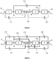
- FIG. 1 A schematic view of a conventional source-follower based filter implemented in a differential configuration is shown in Figure 1 .
- the filter consists of two stages (1, 3; 2, 4) connected between its input (5) and output (7).
- the filter is in a differential configuration and therefore has another set of stages (3, 4). Therefore, the filter includes two pairs of two source-followers stages (1,2) and (3,4) between input nodes (5,6) and output nodes (7,8) (respectively plus and minus as it is a differential configuration), inner nodes (9,10) being defined between the two stages of each pair (1,2; 3,4).
- Two feedback capacitors (11, 12) - here of the same value - are connected in parallel with each pair of stages (1, 2) and (3, 4), between input and output nodes (5, 7) and (6, 8) respectively.
- Two additional capacitors (13, 14) are connected between the two inner nodes (9, 10) (parallel capacitor 13) and output nodes (7, 8) (series capacitor 14), respectively.
- This filter has two zeros and two poles in its transfer function. However, these four parameters are linked to each other, in a way that, when three of them have been selected, the fourth one is determined. This is because this conventional filter has only complex conjugate imaginary zeros, which by nature are interlinked. Thus, the filter of Figure 1 does not offer a sufficient degree of freedom to freely place the zeros on the complex plane and hence does not allow to freely determine the shape of the transfer function.
- FIG. 2 shows a schematic view of the filter according to the present disclosure.
- the filter of Figure 2 comprises additional feedback means (15) and (16), one (15) between the input (5) and the inner node (9) and one (16) between the inner node (9) and the output node (8).
- similar feedback means (18) and (17) are comprised for the other two stages (3) and (4).
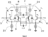
- Figure 3 shows a circuit according to an embodiment of the present disclosure and in line with the schematic view of Figure 2 .
- the filter of Figure 3 which is here a differential filter, is distinguished from the one of Figure 1 by the four additional feedback capacitors Ca and Cc (15-18).
- Two capacitors Ca (15,18) are connected between input node (5) and inner node (9) and between input node (6) and inner node (10).
- Two capacitors Cc (16, 17) are connected between output node (8) and inner node (9) and between output node (7) and inner node (10).
- the first stage of the filter connecting the input node (5) with the inner node (9) comprises a transistor (M1) in a source follower configuration and a current source (21) which defines the operating point of the transistor.
- a second stage comprising a current source (24) and transistor (M4) again in a source follower configuration connects the inner node (9) with the output node (7).
- the merit of the disclosure has been to include, within the filter, a rather important number of feedback means as for instance feedback paths and, particularly, as compared with the filter of the prior art, additional capacitors 15, 18 between input and inner nodes and additional capacitors 16, 17 between inner and output nodes.
- the filter of Figures 2 and 3 are filters with two complex zeros and two complex poles which are independent from each other.
- the transfer function TF of the filter shown in Figures 2 and 3 is given below.
- the TF offers two zeros and two poles - both the nominator and the denominator are of second order.
- the capacitors and the transistor transconductance g m define the location of the poles and zeros.
- TF ⁇ C a + C c C b + C c C a + C 1 g m 2 s 2 + C a ⁇ C b g m s + 1 C a + C c + C 1 + C 2 C b + C c + C 2 C a + C 1 g m 2 s 2 + C b + C a + C 1 g m s + 1
- the degree of freedom is sufficient to place these poles and zeros independently from one another.
- one or more of the capacitors may be implemented as variable capacitors or as configurable banks of capacitors.
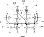
- FIG. 4 An alternative embodiment for the current sources (21-24) of the previous embodiment is shown in Figure 4 .
- a current mirror may be used.
- This current mirror preferably comprises two transistors (M5,M7) whereby transistor M7 senses the current in the second stage and drives transistor M5 to deliver a current to the first stage equal to the one in the second stage.
- transistor M5 and M7 Dependent on the dimensions of the transistor M5 and M7 the ratio between the current in the first stage and the second stage may be chosen.
- the current mirror feeds back the current of the second stage, removing the need to directly connect the drain of the second stage to the source of the first stage. Since the drain of the second stage is now loaded by a node with a low impedance, the linearity of the filter is improved.
Landscapes
- Engineering & Computer Science (AREA)
- Power Engineering (AREA)
- Physics & Mathematics (AREA)
- Nonlinear Science (AREA)
- Networks Using Active Elements (AREA)
- Amplifiers (AREA)
Claims (6)
- Source-Folger-basiertes Filter eines Differentialtyps, das zwei Stufen aufweist, mit zwei Paaren von Source-Folgern pro Stufe, wobei das Filter Folgendes umfasst: eine erste und eine zweite Stufe (1, 3; 2, 4), die jeweils zwei Source-Folger (1, 3; 2, 4) umfassen,
wobei ein Source-Folger (1; 3) in der ersten Stufe (1; 3) mit einem entsprechenden Source-Folger (2; 4) in der zweiten Stufe (2; 4) in Reihe geschaltet ist, und zwischen Eingangsknoten (5, 6) und Ausgangsknoten (7, 8) des Filters, wobei ein innerer Knoten (9, 10) die zwei in Reihe geschalteten Source-Folger (1, 2; 3, 4) elektrisch verbindet und Rückkopplungskondensatoren (11; 12) zwischen dem Eingangsknoten (5, 6) bzw. den Ausgangsknoten (7, 8) angeschlossen sind, wobei das Filter eine Transferfunktion mit mindestens zwei Nullstellen und zwei Polstellen aufweist, wobei das Filter ein zusätzliches Rückkopplungsmittel zum Definieren einer Position der Polstellen und der Nullstellen unabhängig voneinander umfasst,
wobei das zusätzliche Rückkopplungsmittel Kondensatoren (15-18) umfasst, wobei die zusätzlichen Rückkopplungsmittel (15-18) zwischen Eingangsknoten (5, 6) und inneren Knoten (9, 10) und zwischen Ausgangsknoten (7, 8) und inneren Knoten (10; 9) des Filters angeschlossen sind und wobei die Ausgangsknoten (7, 8) durch einen Kondensator (14) verbunden sind. - Filter nach Anspruch 1, wobei jede der zwei Stufen einen Source-Folger-Transistor (1; 2; 3; 4) umfasst, wobei die Source-Folger-Transistoren (1; 2; 3; 4) der zwei Stufen hintereinander geschaltet sind.
- Filter nach einem der Ansprüche 1 und 2, wobei die inneren Knoten (9, 10) durch einen Kondensator (13) verbunden sind.
- Filter nach einem der Ansprüche 1 bis 3, wobei jede der Stufen zwei Stromquellen (21, 23; 22, 24) umfasst.
- Filter nach Anspruch 4, wobei die Stromquelle (21) mindestens einer Stufe als ein Stromspiegel implementiert ist.
- Filter nach einem der Ansprüche 1 bis 5, wobei einer oder mehrere Kondensatoren als variable Kondensatoren oder als konfigurierbare Kondensatorbänke implementiert sind.
Priority Applications (2)
| Application Number | Priority Date | Filing Date | Title |
|---|---|---|---|
| EP13157467.5A EP2773041B1 (de) | 2013-03-01 | 2013-03-01 | Zweistufen-Filter auf Quellenverfolgungsbasis |
| US14/192,551 US9124251B2 (en) | 2013-03-01 | 2014-02-27 | Two stage source-follower based filter |
Applications Claiming Priority (1)
| Application Number | Priority Date | Filing Date | Title |
|---|---|---|---|
| EP13157467.5A EP2773041B1 (de) | 2013-03-01 | 2013-03-01 | Zweistufen-Filter auf Quellenverfolgungsbasis |
Publications (2)
| Publication Number | Publication Date |
|---|---|
| EP2773041A1 EP2773041A1 (de) | 2014-09-03 |
| EP2773041B1 true EP2773041B1 (de) | 2017-05-03 |
Family
ID=47832943
Family Applications (1)
| Application Number | Title | Priority Date | Filing Date |
|---|---|---|---|
| EP13157467.5A Not-in-force EP2773041B1 (de) | 2013-03-01 | 2013-03-01 | Zweistufen-Filter auf Quellenverfolgungsbasis |
Country Status (2)
| Country | Link |
|---|---|
| US (1) | US9124251B2 (de) |
| EP (1) | EP2773041B1 (de) |
Families Citing this family (4)
| Publication number | Priority date | Publication date | Assignee | Title |
|---|---|---|---|---|
| US9520872B2 (en) * | 2014-12-23 | 2016-12-13 | Qualcomm Incorporated | Linear equalizer with variable gain |
| TWI596895B (zh) * | 2016-12-16 | 2017-08-21 | 國立臺灣大學 | 具有超級源極隨耦器的低通濾波器及傳輸零點控制方法 |
| US11689201B2 (en) | 2021-07-26 | 2023-06-27 | Qualcomm Incorporated | Universal serial bus (USB) host data switch with integrated equalizer |
| US12362717B2 (en) | 2022-11-16 | 2025-07-15 | Qualcomm Incorporated | Second-order equalizer for high-speed data lines |
Family Cites Families (5)
| Publication number | Priority date | Publication date | Assignee | Title |
|---|---|---|---|---|
| GB1212671A (en) * | 1966-08-05 | 1970-11-18 | Walter Farrer | Active filters with independent control of the pole and zero locations |
| US4524332A (en) * | 1982-02-10 | 1985-06-18 | Motorola, Inc. | Integrated notch filter |
| JP4652863B2 (ja) * | 2005-03-23 | 2011-03-16 | 富士通セミコンダクター株式会社 | フィルタ回路のq補正 |
| JP2009509447A (ja) | 2005-09-23 | 2009-03-05 | グロナヴ リミテッド | フィルタ回路 |
| EP2429075A1 (de) | 2010-09-13 | 2012-03-14 | Imec | Verstärkerschaltung für einen Sender-Empfänger zur Entfernungsmessung |
-
2013
- 2013-03-01 EP EP13157467.5A patent/EP2773041B1/de not_active Not-in-force
-
2014
- 2014-02-27 US US14/192,551 patent/US9124251B2/en not_active Expired - Fee Related
Also Published As
| Publication number | Publication date |
|---|---|
| US9124251B2 (en) | 2015-09-01 |
| US20140247089A1 (en) | 2014-09-04 |
| EP2773041A1 (de) | 2014-09-03 |
Similar Documents
| Publication | Publication Date | Title |
|---|---|---|
| US7535323B2 (en) | Bulk acoustic wave filter with reduced nonlinear signal distortion | |
| CN102340294B (zh) | 一种四阶有源lc射频带通滤波器 | |
| US9641138B2 (en) | Multipath feedforward band pass amplifier | |
| EP2491653B1 (de) | Entwurf für einen tiefpassfilter | |
| EP2874313B1 (de) | Analoge aktive Tiefpassfilter | |
| RU2453985C1 (ru) | Высокоизбирательный полосовой перестраиваемый lc-фильтр | |
| CN202488406U (zh) | 一种高稳定性可编程增益放大器结构 | |
| TWI442695B (zh) | 在接收器射頻前端達成高選擇性之方法 | |
| US20160164487A1 (en) | Bulk acoustic wave filter | |
| US9148112B2 (en) | Matching circuit system | |
| JP2012175278A (ja) | バンドパスフィルタ及びバンドパスフィルタのキャリブレーション方法 | |
| US9774310B2 (en) | Common mode noise suppressing device | |
| US20190081612A1 (en) | Signal Filtering Using Magnetic Coupling | |
| US9124251B2 (en) | Two stage source-follower based filter | |
| US20180175827A1 (en) | Low-pass filter with super source follower and transmission zero controlling method | |
| US20170141733A1 (en) | Distributed pole-zero compensation for an amplifier | |
| Pantoli et al. | Low voltage high-order agile active filter for microwave applications | |
| US20140369439A1 (en) | Single amplifier filter for constant group delay in radio frequency transmitters | |
| US12068738B2 (en) | Configurable micro-acoustic RF filter | |
| RU2372711C1 (ru) | Полосовой высокоизбирательный lc-фильтр | |
| JP5807762B2 (ja) | 高周波モジュール及びそれを用いた携帯端末 | |
| US7880536B2 (en) | Simplified sallen-key low-pass filter circuit | |
| CN104333339A (zh) | 一种可调变压器 | |
| CN114785297A (zh) | 功率放大器及其输入匹配网络 | |
| Huang et al. | A 100 MHz G m-C bandpass filter chip design for wireless application |
Legal Events
| Date | Code | Title | Description |
|---|---|---|---|
| PUAI | Public reference made under article 153(3) epc to a published international application that has entered the european phase |
Free format text: ORIGINAL CODE: 0009012 |
|
| 17P | Request for examination filed |
Effective date: 20140317 |
|
| AK | Designated contracting states |
Kind code of ref document: A1 Designated state(s): AL AT BE BG CH CY CZ DE DK EE ES FI FR GB GR HR HU IE IS IT LI LT LU LV MC MK MT NL NO PL PT RO RS SE SI SK SM TR |
|
| AX | Request for extension of the european patent |
Extension state: BA ME |
|
| 17Q | First examination report despatched |
Effective date: 20160211 |
|
| GRAP | Despatch of communication of intention to grant a patent |
Free format text: ORIGINAL CODE: EPIDOSNIGR1 |
|
| INTG | Intention to grant announced |
Effective date: 20161025 |
|
| STAA | Information on the status of an ep patent application or granted ep patent |
Free format text: STATUS: GRANT OF PATENT IS INTENDED |
|
| GRAS | Grant fee paid |
Free format text: ORIGINAL CODE: EPIDOSNIGR3 |
|
| GRAA | (expected) grant |
Free format text: ORIGINAL CODE: 0009210 |
|
| STAA | Information on the status of an ep patent application or granted ep patent |
Free format text: STATUS: THE PATENT HAS BEEN GRANTED |
|
| AK | Designated contracting states |
Kind code of ref document: B1 Designated state(s): AL AT BE BG CH CY CZ DE DK EE ES FI FR GB GR HR HU IE IS IT LI LT LU LV MC MK MT NL NO PL PT RO RS SE SI SK SM TR |
|
| REG | Reference to a national code |
Ref country code: GB Ref legal event code: FG4D |
|
| REG | Reference to a national code |
Ref country code: AT Ref legal event code: REF Ref document number: 891031 Country of ref document: AT Kind code of ref document: T Effective date: 20170515 Ref country code: CH Ref legal event code: EP |
|
| REG | Reference to a national code |
Ref country code: IE Ref legal event code: FG4D |
|
| REG | Reference to a national code |
Ref country code: DE Ref legal event code: R096 Ref document number: 602013020485 Country of ref document: DE |
|
| REG | Reference to a national code |
Ref country code: NL Ref legal event code: MP Effective date: 20170503 |
|
| REG | Reference to a national code |
Ref country code: AT Ref legal event code: MK05 Ref document number: 891031 Country of ref document: AT Kind code of ref document: T Effective date: 20170503 |
|
| REG | Reference to a national code |
Ref country code: LT Ref legal event code: MG4D |
|
| PG25 | Lapsed in a contracting state [announced via postgrant information from national office to epo] |
Ref country code: LT Free format text: LAPSE BECAUSE OF FAILURE TO SUBMIT A TRANSLATION OF THE DESCRIPTION OR TO PAY THE FEE WITHIN THE PRESCRIBED TIME-LIMIT Effective date: 20170503 Ref country code: HR Free format text: LAPSE BECAUSE OF FAILURE TO SUBMIT A TRANSLATION OF THE DESCRIPTION OR TO PAY THE FEE WITHIN THE PRESCRIBED TIME-LIMIT Effective date: 20170503 Ref country code: ES Free format text: LAPSE BECAUSE OF FAILURE TO SUBMIT A TRANSLATION OF THE DESCRIPTION OR TO PAY THE FEE WITHIN THE PRESCRIBED TIME-LIMIT Effective date: 20170503 Ref country code: NO Free format text: LAPSE BECAUSE OF FAILURE TO SUBMIT A TRANSLATION OF THE DESCRIPTION OR TO PAY THE FEE WITHIN THE PRESCRIBED TIME-LIMIT Effective date: 20170803 Ref country code: FI Free format text: LAPSE BECAUSE OF FAILURE TO SUBMIT A TRANSLATION OF THE DESCRIPTION OR TO PAY THE FEE WITHIN THE PRESCRIBED TIME-LIMIT Effective date: 20170503 Ref country code: AT Free format text: LAPSE BECAUSE OF FAILURE TO SUBMIT A TRANSLATION OF THE DESCRIPTION OR TO PAY THE FEE WITHIN THE PRESCRIBED TIME-LIMIT Effective date: 20170503 Ref country code: GR Free format text: LAPSE BECAUSE OF FAILURE TO SUBMIT A TRANSLATION OF THE DESCRIPTION OR TO PAY THE FEE WITHIN THE PRESCRIBED TIME-LIMIT Effective date: 20170804 |
|
| PG25 | Lapsed in a contracting state [announced via postgrant information from national office to epo] |
Ref country code: IS Free format text: LAPSE BECAUSE OF FAILURE TO SUBMIT A TRANSLATION OF THE DESCRIPTION OR TO PAY THE FEE WITHIN THE PRESCRIBED TIME-LIMIT Effective date: 20170903 Ref country code: BG Free format text: LAPSE BECAUSE OF FAILURE TO SUBMIT A TRANSLATION OF THE DESCRIPTION OR TO PAY THE FEE WITHIN THE PRESCRIBED TIME-LIMIT Effective date: 20170803 Ref country code: PL Free format text: LAPSE BECAUSE OF FAILURE TO SUBMIT A TRANSLATION OF THE DESCRIPTION OR TO PAY THE FEE WITHIN THE PRESCRIBED TIME-LIMIT Effective date: 20170503 Ref country code: SE Free format text: LAPSE BECAUSE OF FAILURE TO SUBMIT A TRANSLATION OF THE DESCRIPTION OR TO PAY THE FEE WITHIN THE PRESCRIBED TIME-LIMIT Effective date: 20170503 Ref country code: LV Free format text: LAPSE BECAUSE OF FAILURE TO SUBMIT A TRANSLATION OF THE DESCRIPTION OR TO PAY THE FEE WITHIN THE PRESCRIBED TIME-LIMIT Effective date: 20170503 Ref country code: RS Free format text: LAPSE BECAUSE OF FAILURE TO SUBMIT A TRANSLATION OF THE DESCRIPTION OR TO PAY THE FEE WITHIN THE PRESCRIBED TIME-LIMIT Effective date: 20170503 Ref country code: NL Free format text: LAPSE BECAUSE OF FAILURE TO SUBMIT A TRANSLATION OF THE DESCRIPTION OR TO PAY THE FEE WITHIN THE PRESCRIBED TIME-LIMIT Effective date: 20170503 |
|
| RAP2 | Party data changed (patent owner data changed or rights of a patent transferred) |
Owner name: UNIVERSITEIT GENT Owner name: IMEC VZW |
|
| PG25 | Lapsed in a contracting state [announced via postgrant information from national office to epo] |
Ref country code: CZ Free format text: LAPSE BECAUSE OF FAILURE TO SUBMIT A TRANSLATION OF THE DESCRIPTION OR TO PAY THE FEE WITHIN THE PRESCRIBED TIME-LIMIT Effective date: 20170503 Ref country code: SK Free format text: LAPSE BECAUSE OF FAILURE TO SUBMIT A TRANSLATION OF THE DESCRIPTION OR TO PAY THE FEE WITHIN THE PRESCRIBED TIME-LIMIT Effective date: 20170503 Ref country code: EE Free format text: LAPSE BECAUSE OF FAILURE TO SUBMIT A TRANSLATION OF THE DESCRIPTION OR TO PAY THE FEE WITHIN THE PRESCRIBED TIME-LIMIT Effective date: 20170503 Ref country code: RO Free format text: LAPSE BECAUSE OF FAILURE TO SUBMIT A TRANSLATION OF THE DESCRIPTION OR TO PAY THE FEE WITHIN THE PRESCRIBED TIME-LIMIT Effective date: 20170503 Ref country code: DK Free format text: LAPSE BECAUSE OF FAILURE TO SUBMIT A TRANSLATION OF THE DESCRIPTION OR TO PAY THE FEE WITHIN THE PRESCRIBED TIME-LIMIT Effective date: 20170503 |
|
| REG | Reference to a national code |
Ref country code: DE Ref legal event code: R097 Ref document number: 602013020485 Country of ref document: DE |
|
| PG25 | Lapsed in a contracting state [announced via postgrant information from national office to epo] |
Ref country code: IT Free format text: LAPSE BECAUSE OF FAILURE TO SUBMIT A TRANSLATION OF THE DESCRIPTION OR TO PAY THE FEE WITHIN THE PRESCRIBED TIME-LIMIT Effective date: 20170503 Ref country code: SM Free format text: LAPSE BECAUSE OF FAILURE TO SUBMIT A TRANSLATION OF THE DESCRIPTION OR TO PAY THE FEE WITHIN THE PRESCRIBED TIME-LIMIT Effective date: 20170503 |
|
| PLBE | No opposition filed within time limit |
Free format text: ORIGINAL CODE: 0009261 |
|
| STAA | Information on the status of an ep patent application or granted ep patent |
Free format text: STATUS: NO OPPOSITION FILED WITHIN TIME LIMIT |
|
| 26N | No opposition filed |
Effective date: 20180206 |
|
| PG25 | Lapsed in a contracting state [announced via postgrant information from national office to epo] |
Ref country code: SI Free format text: LAPSE BECAUSE OF FAILURE TO SUBMIT A TRANSLATION OF THE DESCRIPTION OR TO PAY THE FEE WITHIN THE PRESCRIBED TIME-LIMIT Effective date: 20170503 |
|
| REG | Reference to a national code |
Ref country code: DE Ref legal event code: R119 Ref document number: 602013020485 Country of ref document: DE |
|
| REG | Reference to a national code |
Ref country code: CH Ref legal event code: PL |
|
| GBPC | Gb: european patent ceased through non-payment of renewal fee |
Effective date: 20180301 |
|
| PG25 | Lapsed in a contracting state [announced via postgrant information from national office to epo] |
Ref country code: MC Free format text: LAPSE BECAUSE OF FAILURE TO SUBMIT A TRANSLATION OF THE DESCRIPTION OR TO PAY THE FEE WITHIN THE PRESCRIBED TIME-LIMIT Effective date: 20170503 |
|
| REG | Reference to a national code |
Ref country code: BE Ref legal event code: MM Effective date: 20180331 |
|
| REG | Reference to a national code |
Ref country code: IE Ref legal event code: MM4A |
|
| PG25 | Lapsed in a contracting state [announced via postgrant information from national office to epo] |
Ref country code: LU Free format text: LAPSE BECAUSE OF NON-PAYMENT OF DUE FEES Effective date: 20180301 |
|
| PG25 | Lapsed in a contracting state [announced via postgrant information from national office to epo] |
Ref country code: IE Free format text: LAPSE BECAUSE OF NON-PAYMENT OF DUE FEES Effective date: 20180301 Ref country code: DE Free format text: LAPSE BECAUSE OF NON-PAYMENT OF DUE FEES Effective date: 20181002 |
|
| PG25 | Lapsed in a contracting state [announced via postgrant information from national office to epo] |
Ref country code: BE Free format text: LAPSE BECAUSE OF NON-PAYMENT OF DUE FEES Effective date: 20180331 Ref country code: LI Free format text: LAPSE BECAUSE OF NON-PAYMENT OF DUE FEES Effective date: 20180331 Ref country code: GB Free format text: LAPSE BECAUSE OF NON-PAYMENT OF DUE FEES Effective date: 20180301 Ref country code: CH Free format text: LAPSE BECAUSE OF NON-PAYMENT OF DUE FEES Effective date: 20180331 |
|
| PG25 | Lapsed in a contracting state [announced via postgrant information from national office to epo] |
Ref country code: FR Free format text: LAPSE BECAUSE OF NON-PAYMENT OF DUE FEES Effective date: 20180331 |
|
| PG25 | Lapsed in a contracting state [announced via postgrant information from national office to epo] |
Ref country code: MT Free format text: LAPSE BECAUSE OF NON-PAYMENT OF DUE FEES Effective date: 20180301 |
|
| PG25 | Lapsed in a contracting state [announced via postgrant information from national office to epo] |
Ref country code: TR Free format text: LAPSE BECAUSE OF FAILURE TO SUBMIT A TRANSLATION OF THE DESCRIPTION OR TO PAY THE FEE WITHIN THE PRESCRIBED TIME-LIMIT Effective date: 20170503 |
|
| PG25 | Lapsed in a contracting state [announced via postgrant information from national office to epo] |
Ref country code: PT Free format text: LAPSE BECAUSE OF FAILURE TO SUBMIT A TRANSLATION OF THE DESCRIPTION OR TO PAY THE FEE WITHIN THE PRESCRIBED TIME-LIMIT Effective date: 20170503 Ref country code: HU Free format text: LAPSE BECAUSE OF FAILURE TO SUBMIT A TRANSLATION OF THE DESCRIPTION OR TO PAY THE FEE WITHIN THE PRESCRIBED TIME-LIMIT; INVALID AB INITIO Effective date: 20130301 |
|
| PG25 | Lapsed in a contracting state [announced via postgrant information from national office to epo] |
Ref country code: CY Free format text: LAPSE BECAUSE OF FAILURE TO SUBMIT A TRANSLATION OF THE DESCRIPTION OR TO PAY THE FEE WITHIN THE PRESCRIBED TIME-LIMIT Effective date: 20170503 Ref country code: MK Free format text: LAPSE BECAUSE OF NON-PAYMENT OF DUE FEES Effective date: 20170503 |
|
| PG25 | Lapsed in a contracting state [announced via postgrant information from national office to epo] |
Ref country code: AL Free format text: LAPSE BECAUSE OF FAILURE TO SUBMIT A TRANSLATION OF THE DESCRIPTION OR TO PAY THE FEE WITHIN THE PRESCRIBED TIME-LIMIT Effective date: 20170503 |