EP2773045B1 - Procédé de correction de désadaptation du signal de sortie d'un convertisseur analogique-numérique à entrelacement temporel - Google Patents
Procédé de correction de désadaptation du signal de sortie d'un convertisseur analogique-numérique à entrelacement temporel Download PDFInfo
- Publication number
- EP2773045B1 EP2773045B1 EP13001057.2A EP13001057A EP2773045B1 EP 2773045 B1 EP2773045 B1 EP 2773045B1 EP 13001057 A EP13001057 A EP 13001057A EP 2773045 B1 EP2773045 B1 EP 2773045B1
- Authority
- EP
- European Patent Office
- Prior art keywords
- mismatch
- spur
- signal
- adc
- output signal
- Prior art date
- Legal status (The legal status is an assumption and is not a legal conclusion. Google has not performed a legal analysis and makes no representation as to the accuracy of the status listed.)
- Active
Links
Images



Classifications
-
- H—ELECTRICITY
- H03—ELECTRONIC CIRCUITRY
- H03M—CODING; DECODING; CODE CONVERSION IN GENERAL
- H03M1/00—Analogue/digital conversion; Digital/analogue conversion
- H03M1/06—Continuously compensating for, or preventing, undesired influence of physical parameters
- H03M1/0617—Continuously compensating for, or preventing, undesired influence of physical parameters characterised by the use of methods or means not specific to a particular type of detrimental influence
-
- H—ELECTRICITY
- H03—ELECTRONIC CIRCUITRY
- H03M—CODING; DECODING; CODE CONVERSION IN GENERAL
- H03M1/00—Analogue/digital conversion; Digital/analogue conversion
- H03M1/12—Analogue/digital converters
- H03M1/1205—Multiplexed conversion systems
- H03M1/121—Interleaved, i.e. using multiple converters or converter parts for one channel
- H03M1/1215—Interleaved, i.e. using multiple converters or converter parts for one channel using time-division multiplexing
Definitions
- DSP digital signal processing
- ADC Analog-to-Digital-Converter
- TI-ADC Time-Interleaved ADC
- any arbitrary number of ADCs can be interleaved to achieve a higher sampling rate while preserving the ADC's effective resolution.
- Each ADC will have a different frequency response, e.g. due to unavoidable manufacturing tolerances, causing the ADCs to have a mismatch to one another. This distorts the signal and restricts the TI-ADC's performance by causing spurs in the spectrum which limit the spurious free dynamic range (SFDR) leading to a loss in the TI-ADC's effective resolution.
- SFDR spurious free dynamic range
- a state-of-the-art publication that addresses adaptive frequency response mismatches correction of 2-channel TI-ADCs is [3]. It can be quoted from the publications [1], [3], [5] that suitable online TI-ADC mismatch identification methods (preferably frequency response mismatch identification) with minimum hardware requirement are of interest and an open challenge.
- IMSB Interleaving-Mismatch-Spur-Band
- M being the number of ADCs operated in parallel during the time-interleaved analog to digital conversion.
- This invention concerns a process according to the independent claim for the adaptive digital mismatch correction of an M-channel TI-ADC.
- This mismatch mitigation involves two main steps. The first step is the mismatch identification and the second step is the mismatch compensation.
- This invention is aimed in particular at the identification method. It involves mapping the time interleaved ADC mismatch problem into an IQ imbalance problem for which dedicated solutions are already well established [6].
- IQ imbalance is a problem present in the Homodyne Receiver (HMR).
- HMR's I- & Q-branch mismatch causes frequency components in I- & Q-branch to differ in magnitude and deviate from the required 90° phase difference. This leads to insufficient conjugate frequency rejection which causes spurs in the spectrum that limits the dynamic range and performance of the HMR.
- the spurs are located at the conjugate frequency position of the desired signal tone. The presence of a spur at the conjugate frequency location can be detected and measured using statistical properties of the complex signal [6].
- a mapping mechanism which converts the TI-ADC problem into an IQ imbalance (cf. IQ mismatch) problem.
- the TI-ADC spurs are placed at the conjugate frequency location of the desired signal tone via frequency shifting. This allows the TI-ADC problem to be treated as an IQ imbalance problem for the purpose of extracting the mismatch. It offers a novel solution for identifying the TI-ADC mismatch and circumvents the challenges of existing techniques.
- the TI-ADC's output signal is real-valued and therefore has a two-sided frequency spectrum.
- an analytical signal which has a one-sided spectrum is generated from this TI-ADC real-valued output. This is done either via e.g. a Hilbert transform or a complex band pass filter and it produces a complex valued signal.
- a person skilled in the art would know that the required frequency shifting can be easily performed using complex signals.
- the analytical signal of the TI-ADC output (the input may be any operational signal) is used to derive various specific mismatch identification signals (MIS).
- MIS mismatch identification signals
- each generated MIS one group of the interleaving spurs are placed onto the conjugate frequency position of the desired signal tones. This produces a scenario present in an IQ imbalance system.
- HOS Higher-order-statistics
- the next step involves the TI-ADC mismatch compensation.
- the compensation structure is kept as coherent as possible to the mismatch identification structure.
- the frequency components are first shifted to the spur positions, then filtered (manipulated in magnitude and in phase) so that they match the interleaving spur component.
- the frequency shifting and filtering operations reconstruct the interleaving mismatch spurs. Once the interleaving spur component has been reconstructed, it is subtracted from the original TI-ADC's output signal. This greatly reduces the TI-ADC's spur level (increasing the SFDR) and recovers the TI-ADC's lost effective resolution.
- This invention's advantage lies in the M-channel TI-ADC mismatch identification, which is done without having to reduce the TI-ADC's usable bandwidth. E.g. it does not require allocating an IMSB in the frequency spectrum for the TI-ADC mismatch spurs as can be observed in reference publications [1], [2], [3], [6]. It is therefore free of the inherent drawbacks related to this method. That means it does not fail to estimate the interleaving mismatch if the signal sampled by the TI-ADC does not have frequency components whose spurs fall into this allocated IMSB. Since no IMSB is required, the TI-ADC's available bandwidth is not reduced.
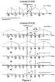
- spur group 305 is confined within the lower half of the 1 st Nyquist zone and spur group 303 in the upper half of the 1 st Nyquist zone for 4-channel TI-ADC 303. Therefore one IMSB would be required in the lower half of the 1 st Nyquist zone and the other in the upper half of the 1 st Nyquist zone to get a reference of all interleaving spurs for the mismatch identification process. As a consequence the usable Nyquist zone becomes segmented.
- mismatch identification signals MIS
- a specific IQ imbalance combination pair is created for each interleaving spur.
- the TI-ADC spurs are placed onto conjugate frequency location of the desired signal tone, as found in the IQ imbalance case.
- This created conjugate pair can be viewed as an IQ imbalance signal.
- This signal is fed into the adaptive IQ imbalance correction block, where the interleaving mismatch parameters are extracted using well-known IQ imbalance correction methods.
- HOS algorithms are deployed to extract the TI-ADC mismatch.
- Another advantage of this invention is the synergy between the identification ( Figure 1 , blocks 101,103,104) and compensation structure ( Figure 1 , blocks 100,101,102, 105).
- This invention offers a complete package of TI-ADC mismatch mitigation.
- the signals generated for the compensation structure are also used for the identification process thus increasing the efficiency and keeping the required computations to a minimum. Therefore the invention is also attractive for an on-chip implementation.
- This invention creates a bridge between TI-ADC and IQ imbalance mismatch correction field of work. It opens up new possibilities for the mismatch identification (via MIS) and circumvents the challenges of existing methods.
- This invention mitigates the M-channel TI-ADC's mismatch related performance degradation (M being the number of ADCs operated in parallel during the time-interleaved analog to digital conversion).
- M being the number of ADCs operated in parallel during the time-interleaved analog to digital conversion.
- the block diagram of the invention is shown in Figure 1 .
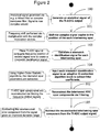
- the operations to be performed are also described in form of a flow chart as seen in Figure 2 .
- the TI-ADC mismatch spurs are mitigated by reconstructing the spur components and subtracting them (in block 105) from the TI-ADC output signal x M (t). This increases the SFDR and restores the TI-ADC's lost effective resolution.
- This invention adaptively finds the filtering coefficients for the block 102.
- This mismatch coefficient identification is done by block 104 using the output of block 103.
- MIS mismatch identification signals
- Each MIS produced is used for one specific interleaving mismatch spur identification. This is done by placing each spur on the conjugate frequency location of the desired signal tone (a concrete example for the spectrum of the MIS is illustrated in Figure 4 ). By doing so, the TI-ADC problem is mapped into an IQ imbalance problem. Now the well-known mismatch spur parameter extraction methods, used in IQ imbalance correction, become applicable.
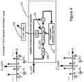
- the IQ imbalance correction is further explained with respect to Figure 4 .
- a person familiar with IQ imbalance correction knows that the IQ imbalance correction involves taking the conjugate of the signal (at block 200), filtering it at IQ correction filter 201 and then subtracting it from the original signal. This reduces the spur level due to the IQ mismatch.
- Optimal scaling coefficients for the filter 201 are obtained in an adaptive manner e.g. by measuring (at block 202) statistical properties of the signal.
- the above mentioned HOS algorithms can be applied which measure statistical properties within the signal that are lost when a spur is located at the conjugate frequency position of the desired signal tone.
- the TI-ADC mismatch spur correction can be done in parallel for all interleaving spur groups.
- the TI-ADC mismatch spur correction can be performed in a sequential manner for each interleaving spur group, for example by cascading the described TI-ADC mismatch correction algorithms. This means that e.g. spur group 304 of Figure 5 can be corrected first and independent of spur groups 303, 305.
- an analytical signal x 2c (t) be constructed using the output of a 2-channel TI-ADC x 2 (t) and its Hilbert Transform (generated in block 100 of Figure 3 ) as shown in eq. 1.
- the frequency response mismatch h 2.1 between the ADCs can be broken down into a gain (cf. magnitude) mismatch A ⁇ and a phase mismatch ⁇ ⁇ .
- x 2c (t) is frequency shifted to the interleaving spur component location via multiplication with the modulation vector (at mixer 101) to produce x 2c_m (t) as shown in eq. 2.
- an IQ imbalance pair is created for the 2-channel TI-ADC spur identification by adding x 2c (t) together with x 2c_m (t), producing z 2_IQ (t) as shown in eq. 3.
- each TI-ADC spur component is located at the conjugate frequency position of a desired signal tone.
- each of the two created signal pairs can be viewed as an IQ imbalance signal pair on which well-known IQ mismatch correction algorithms can be applied, e.g. the HOS based adaptive algorithms.
- the gain and phase mismatch of the TI-ADCs can be extracted.
- a multiple tap version of the algorithm can be used to identify the frequency dependent TI-ADC mismatch and therefore extract the TI-ADC's frequency response mismatch.
- the shifted frequencies x 2c_m (t) are then scaled with the factor h* 2.1 to reconstruct the interleaving mismatch error component.
- These extracted mismatch values are used in the TI-ADC mismatch correction filter 102, which filters x 2c_m (t) to reconstruct the TI-ADC spur component x 2c_m_err (t).
- the real part of reconstructed spur component x 2c_m_err (t) is subtracted at block 105 from x 2 (t) to give x 2_corr (t).
- the signal x 2_corr (t) has a considerably reduced spur level.
- mismatch curves are distinguished.
- the mismatch is frequency independent (curve 404) or with a small frequency dependency (curve 402).
- Both types 402, 404 of mismatches can be corrected using the adaptive correction process according to the invention.
- TI-ADCs with a large bandwidth can have rapidly changing variations in the frequency response mismatch as depicted in curve 403.
- An adaptive filter is not always suitable for following such rapidly changing variations. Therefore a fixed multitap correction filter can be advantageously foreseen to deal with these fast changing variations of curve 403 in the frequency response mismatch. Let this be known as a fixed filter 400.
- the fixed filter design may be done using pilot tones in the laboratory followed by determining the frequency response mismatch over the bandwidth and it can have an optimal number of filter taps required. Such fixed filter is then used in combination with the adaptive correction process described above which corrects slower changing variations (e.g. curve 402) resulting from TI-ADC's frequency response mismatches changes during operation due to various factors.
- the combination of a fixed filter 400 and an adaptive filter 401 is shown in Figure 6 . It offers superior performance for TI-ADCs with a large bandwidth. It is particularly suitable for systems with high performance demand.
Landscapes
- Engineering & Computer Science (AREA)
- Theoretical Computer Science (AREA)
- Analogue/Digital Conversion (AREA)
Claims (4)
- Procédé de correction de désadaptation du signal de sortie d'un convertisseur analogique-numérique à entrelacement temporel, le signal de sortie contenant des composants de fréquence qui comprennent, en plus d'une tonalité de signal souhaitée, un ou plusieurs groupes de composants parasites de désadaptation, ledit procédé consistant :- à générer (100) un signal analytique du signal de sortie du module analogique-numérique à entrelacement temporel, ce qui permet de créer un signal à valeur complexe ;- pour le groupe de composants parasites de désadaptation ou pour chacun des groupes de composants parasites de désadaptation, à décaler (101) la fréquence du signal analytique afin de passer la tonalité de signal souhaitée à l'emplacement de fréquence du groupe de composants parasites de désadaptation correspondant par multiplication avec un vecteur de modulation complexe, ce qui permet de générer des composants de fréquence décalée correspondants ;- à utiliser le signal analytique et les composants de fréquence décalée pour créer (103) un signal d'identification de désadaptation pour chaque groupe de composants parasites de désadaptation en plaçant le groupe de composants parasites de désadaptation correspondant à l'emplacement de fréquence conjugué de la tonalité de signal souhaitée,- à soumettre (104) chaque signal d'identification de désadaptation à un algorithme de correction de désadaptation IQ afin de dériver des paramètres parasites de désadaptation par rapport à un groupe de composants parasites de désadaptation,- à filtrer (102) les composants de fréquence décalée en utilisant les paramètres parasites de désadaptation dérivés par le biais de l'algorithme de correction de désadaptation IQ, ce qui permet de reconstruire le groupe de composants parasites de désadaptation,- à soustraire (105) le groupe de composants parasites de désadaptation reconstruit du signal de sortie du module analogique-numérique à entrelacement temporel.
- Procédé selon la revendication 1, dans lequel la correction de désadaptation du signal de sortie du module analogique-numérique à entrelacement temporel est réalisée en parallèle par rapport à une pluralité de groupes de composants parasites de désadaptation.
- Procédé selon la revendication 1, dans lequel la correction de désadaptation du signal de sortie du module analogique-numérique à entrelacement temporel est réalisée de manière séquentielle par rapport aux groupes de composants parasites de désadaptation individuels.
- Procédé selon l'une des revendications précédentes 1 à 3, réalisé en combinaison avec un autre procédé pour traiter des variations changeant rapidement, ledit autre procédé comprenant un filtrage réalisé par un filtre fixe.
Priority Applications (1)
| Application Number | Priority Date | Filing Date | Title |
|---|---|---|---|
| EP13001057.2A EP2773045B1 (fr) | 2013-03-02 | 2013-03-02 | Procédé de correction de désadaptation du signal de sortie d'un convertisseur analogique-numérique à entrelacement temporel |
Applications Claiming Priority (1)
| Application Number | Priority Date | Filing Date | Title |
|---|---|---|---|
| EP13001057.2A EP2773045B1 (fr) | 2013-03-02 | 2013-03-02 | Procédé de correction de désadaptation du signal de sortie d'un convertisseur analogique-numérique à entrelacement temporel |
Publications (2)
| Publication Number | Publication Date |
|---|---|
| EP2773045A1 EP2773045A1 (fr) | 2014-09-03 |
| EP2773045B1 true EP2773045B1 (fr) | 2019-02-13 |
Family
ID=47844034
Family Applications (1)
| Application Number | Title | Priority Date | Filing Date |
|---|---|---|---|
| EP13001057.2A Active EP2773045B1 (fr) | 2013-03-02 | 2013-03-02 | Procédé de correction de désadaptation du signal de sortie d'un convertisseur analogique-numérique à entrelacement temporel |
Country Status (1)
| Country | Link |
|---|---|
| EP (1) | EP2773045B1 (fr) |
Families Citing this family (9)
| Publication number | Priority date | Publication date | Assignee | Title |
|---|---|---|---|---|
| CN105704070B (zh) * | 2014-11-25 | 2019-06-11 | 深圳市中兴微电子技术有限公司 | 一种终端及其时域内插控制方法和装置 |
| US9641191B1 (en) | 2015-11-12 | 2017-05-02 | Guzik Technical Enterprises | Digital down converter with equalization |
| CN108366037B (zh) * | 2018-01-24 | 2020-09-15 | 佛山市顺德区中山大学研究院 | 基于iq通信收发系统的多通道tiadc失真校正方法 |
| CN108736891B (zh) * | 2018-04-16 | 2021-09-17 | 佛山市顺德区中山大学研究院 | 一种iq和tiadc失配校正系统及方法 |
| WO2020097939A1 (fr) * | 2018-11-16 | 2020-05-22 | 华为技术有限公司 | Procédé de correction d'erreurs et convertisseur analogique/numérique entrelacé dans le temps |
| CN109756227B (zh) * | 2019-01-11 | 2022-12-16 | 北京工业大学 | 一种基于测试信号的tiadc时间误差的半盲校正方法 |
| CN113114241B (zh) * | 2021-03-10 | 2022-04-19 | 电子科技大学 | 一种时间交替架构采集系统中频响失配误差的校正方法 |
| CN114584144B (zh) * | 2022-01-26 | 2023-03-24 | 苏州迅芯微电子有限公司 | 时间交织adc采样时间偏差提取方法、系统及装置 |
| US12418298B2 (en) | 2023-02-10 | 2025-09-16 | Apple Inc. | Localized IQ mismatch measurement and compensation systems and methods |
Family Cites Families (5)
| Publication number | Priority date | Publication date | Assignee | Title |
|---|---|---|---|---|
| US8307284B2 (en) | 2004-03-26 | 2012-11-06 | Ross Video Limited | Method and system for automated control of audio and video sources and a final composite output thereof through a video switcher |
| EP1844550B1 (fr) | 2005-02-04 | 2010-12-08 | Signal Processing Devices Sweden AB | Evaluation d'erreurs de rythme dans un systeme de conversion analogique en numerique a entrelacement temporel |
| US7403875B2 (en) | 2006-04-12 | 2008-07-22 | Infineon Technologies Ag | System for reconstruction of non-uniformly sampled signals |
| WO2008156400A1 (fr) | 2007-06-21 | 2008-12-24 | Signal Processing Devices Sweden Ab | Compensation des erreurs de désadaptation dans un convertisseur analogique / numérique à entrelacement temporel |
| CA2688528C (fr) | 2007-06-21 | 2015-04-14 | Signal Processing Devices Sweden Ab | Compensation des erreurs de desadaptation dans un convertisseur analogique / numerique a entrelacement temporel |
-
2013
- 2013-03-02 EP EP13001057.2A patent/EP2773045B1/fr active Active
Non-Patent Citations (1)
| Title |
|---|
| None * |
Also Published As
| Publication number | Publication date |
|---|---|
| EP2773045A1 (fr) | 2014-09-03 |
Similar Documents
| Publication | Publication Date | Title |
|---|---|---|
| EP2773045B1 (fr) | Procédé de correction de désadaptation du signal de sortie d'un convertisseur analogique-numérique à entrelacement temporel | |
| Ragheb et al. | Expression of Concern: Implementation models for analog-to-information conversion via random sampling | |
| US8463133B1 (en) | Signal framing in a coherent optical receiver | |
| KR101838298B1 (ko) | 타임인터리빙된 아날로그디지털 컨버터를 위한 로버스트 이득 및 위상 캘리브레이션 방법 | |
| EP3675365B1 (fr) | Étalonnage linéaire et non linéaire pour convertisseur numérique-analogique à entrelacement temporel | |
| US9893924B2 (en) | Module for a radio receiver | |
| US6771198B2 (en) | Method and apparatus for converting between analog and digital domains using frequency interleaving | |
| US12009830B2 (en) | Timing skew mismatch calibration for time interleaved analog to digital converters | |
| US10355706B1 (en) | Equalization of sub-DAC frequency response misalignments in time-interleaved high-speed digital to analog converters | |
| US20060232460A1 (en) | Estimation circuit for time-interleaved adc and method thereof | |
| KR102341875B1 (ko) | 송신기 및 수신기와 해당 방법들 | |
| US20160241253A1 (en) | Two-stage digital down-conversion of rf pulses | |
| CN101399930A (zh) | 智能型扫描频道的方法及其相关装置 | |
| KR101879516B1 (ko) | 디지털 디첩 처리 장치 및 방법 | |
| KR20120122972A (ko) | 2?채널 타임?인터리브된 아날로그?디지털 컨버터에서의 샘플?타임 미스매치 에러 캘리브레이션에 대한 그래디언트?기반 접근 | |
| WO2009098641A1 (fr) | Convertisseur de signal | |
| Singh et al. | 2-channel time-interleaved ADC frequency response mismatch correction using adaptive I/Q signal processing | |
| Marelli et al. | Linear LMS compensation for timing mismatch in time-interleaved ADCs | |
| US20080222228A1 (en) | Bank of cascadable digital filters, and reception circuit including such a bank of cascaded filters | |
| Singh et al. | A blind frequency response mismatch correction algorithm for 4-channel time-interleaved ADC | |
| US10855327B2 (en) | Parallelized successive interference cancellation (PSiC) receiver architecture for wireless communications systems | |
| KR101691367B1 (ko) | M채널 TI-ADCs에서 미스매치에 대한 디지털 후면 교정 방법 및 그 장치 | |
| Singh et al. | A novel blind adaptive correction algorithm for 2-channel time-interleaved ADCs | |
| Vogel | A frequency domain method for blind identification of timing mismatches in time-interleaved ADCs | |
| US11469784B2 (en) | Spur estimating receiver system |
Legal Events
| Date | Code | Title | Description |
|---|---|---|---|
| PUAI | Public reference made under article 153(3) epc to a published international application that has entered the european phase |
Free format text: ORIGINAL CODE: 0009012 |
|
| 17P | Request for examination filed |
Effective date: 20130302 |
|
| AK | Designated contracting states |
Kind code of ref document: A1 Designated state(s): AL AT BE BG CH CY CZ DE DK EE ES FI FR GB GR HR HU IE IS IT LI LT LU LV MC MK MT NL NO PL PT RO RS SE SI SK SM TR |
|
| AX | Request for extension of the european patent |
Extension state: BA ME |
|
| R17P | Request for examination filed (corrected) |
Effective date: 20150218 |
|
| RBV | Designated contracting states (corrected) |
Designated state(s): AL AT BE BG CH CY CZ DE DK EE ES FI FR GB GR HR HU IE IS IT LI LT LU LV MC MK MT NL NO PL PT RO RS SE SI SK SM TR |
|
| RAP1 | Party data changed (applicant data changed or rights of an application transferred) |
Owner name: AIRBUS DS ELECTRONICS AND BORDER SECURITY GMBH |
|
| RAP1 | Party data changed (applicant data changed or rights of an application transferred) |
Owner name: HENSOLDT SENSORS GMBH |
|
| GRAP | Despatch of communication of intention to grant a patent |
Free format text: ORIGINAL CODE: EPIDOSNIGR1 |
|
| STAA | Information on the status of an ep patent application or granted ep patent |
Free format text: STATUS: GRANT OF PATENT IS INTENDED |
|
| RIC1 | Information provided on ipc code assigned before grant |
Ipc: H03M 1/06 20060101AFI20181030BHEP Ipc: H03M 1/12 20060101ALN20181030BHEP |
|
| INTG | Intention to grant announced |
Effective date: 20181128 |
|
| GRAS | Grant fee paid |
Free format text: ORIGINAL CODE: EPIDOSNIGR3 |
|
| GRAA | (expected) grant |
Free format text: ORIGINAL CODE: 0009210 |
|
| STAA | Information on the status of an ep patent application or granted ep patent |
Free format text: STATUS: THE PATENT HAS BEEN GRANTED |
|
| AK | Designated contracting states |
Kind code of ref document: B1 Designated state(s): AL AT BE BG CH CY CZ DE DK EE ES FI FR GB GR HR HU IE IS IT LI LT LU LV MC MK MT NL NO PL PT RO RS SE SI SK SM TR |
|
| REG | Reference to a national code |
Ref country code: GB Ref legal event code: FG4D |
|
| REG | Reference to a national code |
Ref country code: CH Ref legal event code: EP Ref country code: AT Ref legal event code: REF Ref document number: 1096812 Country of ref document: AT Kind code of ref document: T Effective date: 20190215 |
|
| REG | Reference to a national code |
Ref country code: IE Ref legal event code: FG4D |
|
| REG | Reference to a national code |
Ref country code: DE Ref legal event code: R096 Ref document number: 602013050692 Country of ref document: DE |
|
| REG | Reference to a national code |
Ref country code: LT Ref legal event code: MG4D |
|
| REG | Reference to a national code |
Ref country code: NL Ref legal event code: MP Effective date: 20190213 |
|
| PG25 | Lapsed in a contracting state [announced via postgrant information from national office to epo] |
Ref country code: NL Free format text: LAPSE BECAUSE OF FAILURE TO SUBMIT A TRANSLATION OF THE DESCRIPTION OR TO PAY THE FEE WITHIN THE PRESCRIBED TIME-LIMIT Effective date: 20190213 Ref country code: FI Free format text: LAPSE BECAUSE OF FAILURE TO SUBMIT A TRANSLATION OF THE DESCRIPTION OR TO PAY THE FEE WITHIN THE PRESCRIBED TIME-LIMIT Effective date: 20190213 Ref country code: LT Free format text: LAPSE BECAUSE OF FAILURE TO SUBMIT A TRANSLATION OF THE DESCRIPTION OR TO PAY THE FEE WITHIN THE PRESCRIBED TIME-LIMIT Effective date: 20190213 Ref country code: PT Free format text: LAPSE BECAUSE OF FAILURE TO SUBMIT A TRANSLATION OF THE DESCRIPTION OR TO PAY THE FEE WITHIN THE PRESCRIBED TIME-LIMIT Effective date: 20190613 Ref country code: SE Free format text: LAPSE BECAUSE OF FAILURE TO SUBMIT A TRANSLATION OF THE DESCRIPTION OR TO PAY THE FEE WITHIN THE PRESCRIBED TIME-LIMIT Effective date: 20190213 Ref country code: NO Free format text: LAPSE BECAUSE OF FAILURE TO SUBMIT A TRANSLATION OF THE DESCRIPTION OR TO PAY THE FEE WITHIN THE PRESCRIBED TIME-LIMIT Effective date: 20190513 |
|
| PG25 | Lapsed in a contracting state [announced via postgrant information from national office to epo] |
Ref country code: HR Free format text: LAPSE BECAUSE OF FAILURE TO SUBMIT A TRANSLATION OF THE DESCRIPTION OR TO PAY THE FEE WITHIN THE PRESCRIBED TIME-LIMIT Effective date: 20190213 Ref country code: RS Free format text: LAPSE BECAUSE OF FAILURE TO SUBMIT A TRANSLATION OF THE DESCRIPTION OR TO PAY THE FEE WITHIN THE PRESCRIBED TIME-LIMIT Effective date: 20190213 Ref country code: BG Free format text: LAPSE BECAUSE OF FAILURE TO SUBMIT A TRANSLATION OF THE DESCRIPTION OR TO PAY THE FEE WITHIN THE PRESCRIBED TIME-LIMIT Effective date: 20190513 Ref country code: LV Free format text: LAPSE BECAUSE OF FAILURE TO SUBMIT A TRANSLATION OF THE DESCRIPTION OR TO PAY THE FEE WITHIN THE PRESCRIBED TIME-LIMIT Effective date: 20190213 Ref country code: GR Free format text: LAPSE BECAUSE OF FAILURE TO SUBMIT A TRANSLATION OF THE DESCRIPTION OR TO PAY THE FEE WITHIN THE PRESCRIBED TIME-LIMIT Effective date: 20190514 Ref country code: IS Free format text: LAPSE BECAUSE OF FAILURE TO SUBMIT A TRANSLATION OF THE DESCRIPTION OR TO PAY THE FEE WITHIN THE PRESCRIBED TIME-LIMIT Effective date: 20190613 |
|
| REG | Reference to a national code |
Ref country code: AT Ref legal event code: MK05 Ref document number: 1096812 Country of ref document: AT Kind code of ref document: T Effective date: 20190213 |
|
| PG25 | Lapsed in a contracting state [announced via postgrant information from national office to epo] |
Ref country code: AL Free format text: LAPSE BECAUSE OF FAILURE TO SUBMIT A TRANSLATION OF THE DESCRIPTION OR TO PAY THE FEE WITHIN THE PRESCRIBED TIME-LIMIT Effective date: 20190213 Ref country code: DK Free format text: LAPSE BECAUSE OF FAILURE TO SUBMIT A TRANSLATION OF THE DESCRIPTION OR TO PAY THE FEE WITHIN THE PRESCRIBED TIME-LIMIT Effective date: 20190213 Ref country code: IT Free format text: LAPSE BECAUSE OF FAILURE TO SUBMIT A TRANSLATION OF THE DESCRIPTION OR TO PAY THE FEE WITHIN THE PRESCRIBED TIME-LIMIT Effective date: 20190213 Ref country code: EE Free format text: LAPSE BECAUSE OF FAILURE TO SUBMIT A TRANSLATION OF THE DESCRIPTION OR TO PAY THE FEE WITHIN THE PRESCRIBED TIME-LIMIT Effective date: 20190213 Ref country code: SK Free format text: LAPSE BECAUSE OF FAILURE TO SUBMIT A TRANSLATION OF THE DESCRIPTION OR TO PAY THE FEE WITHIN THE PRESCRIBED TIME-LIMIT Effective date: 20190213 Ref country code: CZ Free format text: LAPSE BECAUSE OF FAILURE TO SUBMIT A TRANSLATION OF THE DESCRIPTION OR TO PAY THE FEE WITHIN THE PRESCRIBED TIME-LIMIT Effective date: 20190213 Ref country code: RO Free format text: LAPSE BECAUSE OF FAILURE TO SUBMIT A TRANSLATION OF THE DESCRIPTION OR TO PAY THE FEE WITHIN THE PRESCRIBED TIME-LIMIT Effective date: 20190213 Ref country code: ES Free format text: LAPSE BECAUSE OF FAILURE TO SUBMIT A TRANSLATION OF THE DESCRIPTION OR TO PAY THE FEE WITHIN THE PRESCRIBED TIME-LIMIT Effective date: 20190213 |
|
| REG | Reference to a national code |
Ref country code: CH Ref legal event code: PL |
|
| REG | Reference to a national code |
Ref country code: DE Ref legal event code: R097 Ref document number: 602013050692 Country of ref document: DE |
|
| PG25 | Lapsed in a contracting state [announced via postgrant information from national office to epo] |
Ref country code: PL Free format text: LAPSE BECAUSE OF FAILURE TO SUBMIT A TRANSLATION OF THE DESCRIPTION OR TO PAY THE FEE WITHIN THE PRESCRIBED TIME-LIMIT Effective date: 20190213 Ref country code: SM Free format text: LAPSE BECAUSE OF FAILURE TO SUBMIT A TRANSLATION OF THE DESCRIPTION OR TO PAY THE FEE WITHIN THE PRESCRIBED TIME-LIMIT Effective date: 20190213 Ref country code: LU Free format text: LAPSE BECAUSE OF NON-PAYMENT OF DUE FEES Effective date: 20190302 |
|
| REG | Reference to a national code |
Ref country code: BE Ref legal event code: MM Effective date: 20190331 |
|
| PLBE | No opposition filed within time limit |
Free format text: ORIGINAL CODE: 0009261 |
|
| STAA | Information on the status of an ep patent application or granted ep patent |
Free format text: STATUS: NO OPPOSITION FILED WITHIN TIME LIMIT |
|
| PG25 | Lapsed in a contracting state [announced via postgrant information from national office to epo] |
Ref country code: MC Free format text: LAPSE BECAUSE OF FAILURE TO SUBMIT A TRANSLATION OF THE DESCRIPTION OR TO PAY THE FEE WITHIN THE PRESCRIBED TIME-LIMIT Effective date: 20190213 Ref country code: AT Free format text: LAPSE BECAUSE OF FAILURE TO SUBMIT A TRANSLATION OF THE DESCRIPTION OR TO PAY THE FEE WITHIN THE PRESCRIBED TIME-LIMIT Effective date: 20190213 |
|
| 26N | No opposition filed |
Effective date: 20191114 |
|
| PG25 | Lapsed in a contracting state [announced via postgrant information from national office to epo] |
Ref country code: IE Free format text: LAPSE BECAUSE OF NON-PAYMENT OF DUE FEES Effective date: 20190302 Ref country code: CH Free format text: LAPSE BECAUSE OF NON-PAYMENT OF DUE FEES Effective date: 20190331 Ref country code: LI Free format text: LAPSE BECAUSE OF NON-PAYMENT OF DUE FEES Effective date: 20190331 |
|
| PG25 | Lapsed in a contracting state [announced via postgrant information from national office to epo] |
Ref country code: SI Free format text: LAPSE BECAUSE OF FAILURE TO SUBMIT A TRANSLATION OF THE DESCRIPTION OR TO PAY THE FEE WITHIN THE PRESCRIBED TIME-LIMIT Effective date: 20190213 Ref country code: BE Free format text: LAPSE BECAUSE OF NON-PAYMENT OF DUE FEES Effective date: 20190331 |
|
| PG25 | Lapsed in a contracting state [announced via postgrant information from national office to epo] |
Ref country code: TR Free format text: LAPSE BECAUSE OF FAILURE TO SUBMIT A TRANSLATION OF THE DESCRIPTION OR TO PAY THE FEE WITHIN THE PRESCRIBED TIME-LIMIT Effective date: 20190213 |
|
| PG25 | Lapsed in a contracting state [announced via postgrant information from national office to epo] |
Ref country code: MT Free format text: LAPSE BECAUSE OF NON-PAYMENT OF DUE FEES Effective date: 20190302 |
|
| PG25 | Lapsed in a contracting state [announced via postgrant information from national office to epo] |
Ref country code: CY Free format text: LAPSE BECAUSE OF FAILURE TO SUBMIT A TRANSLATION OF THE DESCRIPTION OR TO PAY THE FEE WITHIN THE PRESCRIBED TIME-LIMIT Effective date: 20190213 |
|
| PG25 | Lapsed in a contracting state [announced via postgrant information from national office to epo] |
Ref country code: HU Free format text: LAPSE BECAUSE OF FAILURE TO SUBMIT A TRANSLATION OF THE DESCRIPTION OR TO PAY THE FEE WITHIN THE PRESCRIBED TIME-LIMIT; INVALID AB INITIO Effective date: 20130302 |
|
| PG25 | Lapsed in a contracting state [announced via postgrant information from national office to epo] |
Ref country code: MK Free format text: LAPSE BECAUSE OF FAILURE TO SUBMIT A TRANSLATION OF THE DESCRIPTION OR TO PAY THE FEE WITHIN THE PRESCRIBED TIME-LIMIT Effective date: 20190213 |
|
| PGFP | Annual fee paid to national office [announced via postgrant information from national office to epo] |
Ref country code: GB Payment date: 20260324 Year of fee payment: 14 |
|
| PGFP | Annual fee paid to national office [announced via postgrant information from national office to epo] |
Ref country code: DE Payment date: 20260320 Year of fee payment: 14 |
|
| PGFP | Annual fee paid to national office [announced via postgrant information from national office to epo] |
Ref country code: FR Payment date: 20260325 Year of fee payment: 14 |