EP2775263A2 - Analoge Schnittstellenverarbeitungsschaltung mit hoher Genauigkeit - Google Patents
Analoge Schnittstellenverarbeitungsschaltung mit hoher Genauigkeit Download PDFInfo
- Publication number
- EP2775263A2 EP2775263A2 EP14156579.6A EP14156579A EP2775263A2 EP 2775263 A2 EP2775263 A2 EP 2775263A2 EP 14156579 A EP14156579 A EP 14156579A EP 2775263 A2 EP2775263 A2 EP 2775263A2
- Authority
- EP
- European Patent Office
- Prior art keywords
- signal processing
- sensor
- interfaces
- biasing voltage
- interface
- Prior art date
- Legal status (The legal status is an assumption and is not a legal conclusion. Google has not performed a legal analysis and makes no representation as to the accuracy of the status listed.)
- Granted
Links
Images



Classifications
-
- H—ELECTRICITY
- H03—ELECTRONIC CIRCUITRY
- H03K—PULSE TECHNIQUE
- H03K17/00—Electronic switching or gating, i.e. not by contact-making and –breaking
- H03K17/14—Modifications for compensating variations of physical values, e.g. of temperature
- H03K17/145—Modifications for compensating variations of physical values, e.g. of temperature in field-effect transistor switches
-
- G—PHYSICS
- G01—MEASURING; TESTING
- G01D—MEASURING NOT SPECIALLY ADAPTED FOR A SPECIFIC VARIABLE; ARRANGEMENTS FOR MEASURING TWO OR MORE VARIABLES NOT COVERED IN A SINGLE OTHER SUBCLASS; TARIFF METERING APPARATUS; MEASURING OR TESTING NOT OTHERWISE PROVIDED FOR
- G01D3/00—Indicating or recording apparatus with provision for the special purposes referred to in the subgroups
- G01D3/028—Indicating or recording apparatus with provision for the special purposes referred to in the subgroups mitigating undesired influences, e.g. temperature, pressure
Definitions
- the present disclosure relates generally to signal processing, and more particularly to a high accuracy analog interface processing circuit.
- Aerospace sensor system designs such as those used to monitor and control commercial aircraft, require some sensor systems to be measured at an extremely high accuracy to prevent control errors.
- one such system is a pressure system. It is understood that the accuracy of some sensor types adjusts depending on the temperature at which the sensor and the associated circuitry is operating. As a result of the extreme levels accuracy required, and the high temperature variations the sensor circuitry experiences during engine operation, the sensor system is calibrated including temperature calibrations of the sensor and the associated circuitry.
- a sensor processing circuit including a first and second signal processing interface, a processing system connected to an output of each of the first and second signal processing interfaces, a biasing voltage source switchably coupled to the first signal processing interface via a first switch assembly and switchably coupled to the second signal processing interface via a second switch assembly, and a first control output of the processing system controllably coupled to the first switch assembly and a second control output of the processing system controllably couple to the second switch assembly.
- Also disclosed is a method for processing sensor inputs of a sensor system including the steps of: receiving a sensor signal at least two signal processing interfaces, connecting a first of the at least two signal processing interfaces to a biasing voltage source, thereby causing the first signal processing interface to pass a sensor signal to a signal processor, disconnecting the first of the at least two signal processing interfaces from the biasing voltage and connecting a second of the signal processing interfaces to the biasing voltage while the sensor system is operating at a high temperature, thereby counteracting an ionic contamination of said first of said at least two signal processing interfaces.
- an aircraft sensor configuration including at least one analog sensor, a first and second signal processing interface, a processing system connected to an output of each of the first and second signal processing interfaces, a biasing voltage source switchably coupled to the first signal processing interface via a first switch assembly and switchably coupled to the second signal processing interface via a second switch assembly, and a first control output of the processing system controllably coupled to the first switch assembly and a second control output of the processing system controllably couple to the second switch assembly.
- Figure 1 illustrates an example aircraft 10 including a sensor 20 on an aircraft engine 40.
- the sensor 20 is connected to a controller 50, such as a signal processor, via a signal processing interface 30 and a sensor wire 22.
- a controller 50 such as a signal processor
- Some engine systems require sensed information, such as pressure, to be sensed at an extremely high accuracy using analog sensors 20.
- Operation of the sensor interfaces 30 connecting the signal wire 22 from the sensor 20 to the controller 50 (the signal processor) at extreme temperatures, such as those typically found in an operating jet engine 40, can exacerbate the affects of ionic contamination that occurs in the sensor interface 30.
- the ionic contamination affects the sensor readings, potentially moving the readings out of allowed tolerances.
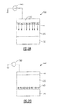
- Figure 2A illustrates a PN junction 100 within an example sensor interface using a gate material layer 110 positioned on an oxide material layer 120.
- the oxide material layer 120 is attached to a substrate 130, such as silicon.
- This arrangement is a standard PN junction arrangement.
- a biasing voltage source 150 is switchably connected to the sensor interface 100. When the biasing voltage source 150 is providing power to the sensor interface, sensor signals entering the sensor interface are passed to the controller 50. Conversely, when the biasing voltage 150 is switched off (disconnected from the sensor interface), the sensor interface does not pass sensor signals to the controller 50.
- ions 140 in the oxide material layer 120 that are normally located near the gate material layer 110 begin to migrate toward the substrate 130. Exposure to high temperatures, such as those experienced in a turbine engine, causes the ions 140 to migrate faster. As the ions 140 migrate, the sensor readings are affected, resulting in ionic contamination.
- Figure 2B illustrates the same PN junction 100 of the sensor interface illustrated in Figure 2A , with like numerals indicating like elements.
- the illustration of Figure 2B shows the ions 140 in position after the PN junction 100 has been biased for a sufficient time period to allow all the ions 140 to migrate to the substrate side of the oxide material layer 120. Ordinarily, once the ions 140 have migrated, it takes a significant time period for the ions 140 to migrate back to the original positions when the PN junction 100 is unbiased.
- the ions 140 migrate back to their original positions significantly faster when the PN junction 100 is unbiased at high temperatures, than when the PN junction 100 is unbiased at standard or low temperatures.
- the rate at which the ions 140 migrate back to their original positions when the PN junction is unbiased at extremely high temperatures is orders of magnitude higher than the rate of ion migration in a biased sensor interface 100 operating at the same temperature. This relationship causes ionic contamination in an unbiased PN junction 100 to correct at a significantly faster rate than it occurs in a biased PN junction 100 at high temperatures.
- FIG. 3 schematically illustrates a highly accurate sensor arrangement 200 utilizing the above described ionic contamination properties to counteract the affects of ionic contamination and achieve a highly accurate sensor arrangement 200 that remains within tolerances at high temperatures.
- the sensor arrangement 200 includes an analog sensor 210 that outputs a sensor signal to two independent signal processing interfaces 222, 224.
- Each of the signal processing interfaces 222, 224 is connected to a dedicated analog to digital converter 232, 234, which converts the sensor signal to a digital signal readable by a processing system 240, such as a controller.
- Each of the signal processing interfaces 222, 224 is also switchably connected to a biasing voltage source 250 via a switch 252, 254.
- the switches 252, 254 are connected to the processing system 240, and the processing system 240 controls the connection between the biasing voltage source 250 and each of the signal processing interfaces 222, 224. In alternate configurations, the switches 252, 254 can be controlled by a separate controller.
- At least one switch 252, 254 is closed at any given time, thereby resulting in one of the signal processing interfaces 222, 224 being biased at all times.
- the biased signal processing interface 222, 224 is alternated between the two signal processing interfaces 222, 224.
- the length of time each signal processing interface 222, 224 is biased is significantly shorter than the length of time required for the ionic contamination to place the signal processing interface 222, 224 out of tolerance.
- the time period required for the signal processing interface 222, 224 to be contaminated out of tolerances is one hour, the signal processing interfaces 222, 224 can be alternated with each interface 222, 224 being biased for five minutes before switching to the other signal processing interface 222, 224.
- the actual biasing time for a practical system will vary depending on design parameters and is not limited to five minutes.
- each signal processing interface 222, 224 returns to an uncontaminated state after being unbiased in significantly less time than it took for the ionic contamination to occur.
- the unbiased signal processing interface 222, 224 will return to the unbiased state well before it is biased again as a result of the timed alternating of the biased signal processing interface 222, 224. It is further understood based upon the above described system that additional signal processing interfaces 222, 224 can be included beyond two and achieve the same affect.
- Figure 4 schematically illustrates an alternate example arrangement for the sensor arrangement 200 illustrated in Figure 3 , with like numerals indicating like elements.
- the example sensor arrangement 200 of Figure 4 includes an additional sensor 212 beyond the first sensor 210.
- the additional sensor 212 and the original sensor 210 are identical sensors and provide identical readings.
- the incorporation of the additional sensor 212 adds redundancy to the system 200, further increasing its robustness.
- Figure 5 illustrates a flowchart demonstrating a method for operating the sensor arrangements 200 illustrated in Figures 3 and 4 .
- Instructions for causing the sensor arrangement to perform the method can be stored in the processing system 240 on a memory.
- the sensor 210, 212 senses an engine property, such as pressure, in a "Sense Property" step 410.
- the sensor 210, 212 transmits the sensed value to each of the signal processing interfaces 222, 224 in the example of Figure 3 and to the corresponding signal processing interface 222, 224 in the example of Figure 4 in a "Transmit Signal to Processing Interfaces" step 420.
- the biasing voltage source 250 is connected to one of the signal processing interfaces 222, 224, biasing the signal processing interface and causing the signal processing interface 222, 224 to transmit the sensor signal from the sensor 210, 212 to the A/D converters 232, 234 and the processing system 240 in a "Bias One Signal Processing Interface" step 430.
- the biasing of the signal processing interface also causes the biased signal processing interface 222, 224 to undergo ionic contamination, reducing the accuracy of the sensor 210, 212.
- the processing system 240 delays action for a set time period in a "Delay Action” step 440.
- the delay allows the currently biased signal processing interface 222, 224 to continue operating while the signal processing interface 222, 224 is within tolerances, without requiring an immediate switch.
- the processing system 240 disconnects the biasing voltage source 250 from the currently operating signal processing interface in a "Remove Bias From First Signal Processing Interface” step 450 and applies a bias to the second signal processing interface 222, 224 in a "Bias Second Signal Processing Interface” step 460.
- the "Remove Bias From First Signal Processing Interface” step 450 and the "Bias Second Signal Processing Interface” step 460 are performed simultaneously or approximately simultaneously, thereby ensuring an uninterrupted flow of sensor readings to the processing system 240.
- the method 400 for operating the sensor arrangement 200 then repeats the "Delay Action” step 440, "Remove Bias From First Signal Processing Interface” step 450 and the “Bias Second Signal Processing Interface” step 460 for as long as the sensor 210 is operating.
- the processing system 240 can detect when the ionic contamination of the operating signal processing interface 222, 224 has exceed an allowable threshold by checking the received sensor signal for errors, sensing the signal processing interface 222, 224, or any other method.
- the processing system 240 can unbias and rebias the signal processing interfaces whenever the current operating signal processing interface 222, 224 exceeds the contamination threshold rather then relying on a set timer, as in the above example.
- the alternate example achieves the same effect of allowing the ionic contamination in the signal processing interfaces to correct while at the same time providing a functional highly accurate sensor reading.
Landscapes
- Physics & Mathematics (AREA)
- General Physics & Mathematics (AREA)
- Arrangements For Transmission Of Measured Signals (AREA)
- Analogue/Digital Conversion (AREA)
- Semiconductor Integrated Circuits (AREA)
- Measuring Fluid Pressure (AREA)
Applications Claiming Priority (1)
| Application Number | Priority Date | Filing Date | Title |
|---|---|---|---|
| US13/789,813 US8786361B1 (en) | 2013-03-08 | 2013-03-08 | High accuracy analog interface processing circuit |
Publications (3)
| Publication Number | Publication Date |
|---|---|
| EP2775263A2 true EP2775263A2 (de) | 2014-09-10 |
| EP2775263A3 EP2775263A3 (de) | 2017-05-03 |
| EP2775263B1 EP2775263B1 (de) | 2019-07-24 |
Family
ID=50193237
Family Applications (1)
| Application Number | Title | Priority Date | Filing Date |
|---|---|---|---|
| EP14156579.6A Active EP2775263B1 (de) | 2013-03-08 | 2014-02-25 | Analoge Schnittstellenverarbeitungsschaltung mit hoher Genauigkeit |
Country Status (2)
| Country | Link |
|---|---|
| US (1) | US8786361B1 (de) |
| EP (1) | EP2775263B1 (de) |
Families Citing this family (1)
| Publication number | Priority date | Publication date | Assignee | Title |
|---|---|---|---|---|
| US9735768B2 (en) * | 2013-07-31 | 2017-08-15 | Fairchild Semiconductor Corporation | Load balancing in discrete devices |
Family Cites Families (19)
| Publication number | Priority date | Publication date | Assignee | Title |
|---|---|---|---|---|
| US4340881A (en) | 1980-06-12 | 1982-07-20 | United Technologies Corporation | Universal analog signal to digital signal interface |
| GB2234069B (en) * | 1988-10-28 | 1992-08-12 | Motorola Inc | Sensor arrangement |
| EP0738011B1 (de) | 1995-04-12 | 2014-12-10 | Fuji Electric Co., Ltd. | Integrierter Hochspannungsschaltkreis, Hochspannungsübergangsabschluss- struktur und MIS-Hochspannungstransistor |
| DE19711215C1 (de) * | 1997-03-18 | 1998-05-07 | Heidenhain Gmbh Dr Johannes | Verfahren und Vorrichtung zur Umschaltung zwischen verschiedenen Ausgangssignal-Arten einer Positionsmeßeinrichtung |
| KR100247964B1 (ko) * | 1997-07-01 | 2000-03-15 | 윤종용 | 자동 문턱값 제어를 이용한 피크 검출기와 그 방법 |
| US6456145B1 (en) * | 2000-09-28 | 2002-09-24 | Koninklijke Philips Electronics N.V. | Non-linear signal correction |
| JP2002135234A (ja) * | 2000-10-20 | 2002-05-10 | Mitsubishi Electric Corp | スキュー調整回路 |
| US6969978B2 (en) * | 2003-03-17 | 2005-11-29 | Rf Micro Devices, Inc. | DC-DC converter with reduced electromagnetic interference |
| US7157895B2 (en) * | 2003-11-04 | 2007-01-02 | Hewlett-Packard Development Company, L.P. | Systems and methods for generating a current |
| US7692179B2 (en) | 2004-07-09 | 2010-04-06 | Hewlett-Packard Development Company, L.P. | Nanowire device with (111) vertical sidewalls and method of fabrication |
| JP2007064755A (ja) * | 2005-08-30 | 2007-03-15 | Samutaku Kk | エンコーダの信号処理回路 |
| JP2009164980A (ja) * | 2008-01-09 | 2009-07-23 | Nsc Co Ltd | 受信機 |
| KR20100052110A (ko) * | 2008-11-10 | 2010-05-19 | 삼성전자주식회사 | 액티브 필터 및 이를 포함하는 델타-시그마 변조기 |
| JP5503990B2 (ja) * | 2010-02-02 | 2014-05-28 | ローム株式会社 | 位相ロックループ回路およびそれを用いた電子機器 |
| US8419273B2 (en) | 2010-05-03 | 2013-04-16 | Sharp Kabushiki Kaisha | Array element for temperature sensor array circuit, temperature sensor array circuit utilizing such array element, and AM-EWOD device including such a temperature sensor array circuit |
| US20120185116A1 (en) | 2011-01-14 | 2012-07-19 | Hamilton Sundstrand Corporation | Integrated bleed and engine controller |
| JP2012174878A (ja) | 2011-02-22 | 2012-09-10 | Hitachi Ltd | 半導体装置、及びそれを用いた装置 |
| US8558296B2 (en) | 2011-03-23 | 2013-10-15 | Texas Instruments Incorporated | Low leakage capacitor for analog floating-gate integrated circuits |
| KR20130025217A (ko) * | 2011-09-01 | 2013-03-11 | 삼성전기주식회사 | 역률 보상 제어 장치 및 그의 제로 커런트 검출 방법 |
-
2013
- 2013-03-08 US US13/789,813 patent/US8786361B1/en active Active
-
2014
- 2014-02-25 EP EP14156579.6A patent/EP2775263B1/de active Active
Non-Patent Citations (1)
| Title |
|---|
| None |
Also Published As
| Publication number | Publication date |
|---|---|
| US8786361B1 (en) | 2014-07-22 |
| EP2775263A3 (de) | 2017-05-03 |
| EP2775263B1 (de) | 2019-07-24 |
Similar Documents
| Publication | Publication Date | Title |
|---|---|---|
| JP4908608B2 (ja) | 電気負荷の電流制御装置 | |
| US10309841B2 (en) | Temperature detecting apparatus | |
| EP2343786A2 (de) | Schaltungsfehlerdetektionsvorrichtung und -verfahren | |
| EP2924404A1 (de) | Thermoelementmodul mit Drahtwiderstandskompensation | |
| KR101173752B1 (ko) | 항공기의 열선장비 감시장치 | |
| KR102326384B1 (ko) | 전자부품 핸들링 장치 및 전자부품 시험장치 | |
| CA2809659A1 (en) | Process fluid temperature measurement | |
| JP6267866B2 (ja) | 絶縁状態検出装置 | |
| EP3070446B1 (de) | Thermische drahttestschaltung und drahttestverfahren | |
| WO2010125733A1 (ja) | 電流制御装置及び保護装置 | |
| US11022481B2 (en) | Load cell having compensation of temperature differences | |
| EP2966419A1 (de) | Heissflüssigkeitsmessvorrichtung | |
| US8864373B2 (en) | Small highly accurate battery temperature monitoring circuit | |
| US8388224B2 (en) | Engine turbine temperature measurement | |
| US8786361B1 (en) | High accuracy analog interface processing circuit | |
| US20180141566A1 (en) | On-Board Control Device, On-Board Integrated Circuit | |
| CN104823069B (zh) | 利用二极管检波器的内部校准的功率测量装置 | |
| EP2579411A1 (de) | Schutzrelaisvorrichtung | |
| US9574925B2 (en) | Fluid measurement device having a circuit for precise flow measurement | |
| US20100052705A1 (en) | Device for detecting the state of a switch | |
| WO2016031269A1 (ja) | 地絡検出装置および地絡検出方法 | |
| EP3124990B1 (de) | Stromsensor mit dynamischer kalibrierung | |
| EP2767839A2 (de) | Detektor des quadratischen Mittelwerts und Schalter | |
| CN115361018B (zh) | 一种adc校正电路 | |
| CN118671567A (zh) | 一种卫星通用热控等效电路、等效器及等效方法 |
Legal Events
| Date | Code | Title | Description |
|---|---|---|---|
| PUAI | Public reference made under article 153(3) epc to a published international application that has entered the european phase |
Free format text: ORIGINAL CODE: 0009012 |
|
| 17P | Request for examination filed |
Effective date: 20140225 |
|
| AK | Designated contracting states |
Kind code of ref document: A2 Designated state(s): AL AT BE BG CH CY CZ DE DK EE ES FI FR GB GR HR HU IE IS IT LI LT LU LV MC MK MT NL NO PL PT RO RS SE SI SK SM TR |
|
| AX | Request for extension of the european patent |
Extension state: BA ME |
|
| PUAL | Search report despatched |
Free format text: ORIGINAL CODE: 0009013 |
|
| AK | Designated contracting states |
Kind code of ref document: A3 Designated state(s): AL AT BE BG CH CY CZ DE DK EE ES FI FR GB GR HR HU IE IS IT LI LT LU LV MC MK MT NL NO PL PT RO RS SE SI SK SM TR |
|
| AX | Request for extension of the european patent |
Extension state: BA ME |
|
| RIC1 | Information provided on ipc code assigned before grant |
Ipc: G01D 3/028 20060101AFI20170328BHEP |
|
| STAA | Information on the status of an ep patent application or granted ep patent |
Free format text: STATUS: REQUEST FOR EXAMINATION WAS MADE |
|
| R17P | Request for examination filed (corrected) |
Effective date: 20171103 |
|
| RBV | Designated contracting states (corrected) |
Designated state(s): AL AT BE BG CH CY CZ DE DK EE ES FI FR GB GR HR HU IE IS IT LI LT LU LV MC MK MT NL NO PL PT RO RS SE SI SK SM TR |
|
| STAA | Information on the status of an ep patent application or granted ep patent |
Free format text: STATUS: EXAMINATION IS IN PROGRESS |
|
| 17Q | First examination report despatched |
Effective date: 20181026 |
|
| GRAP | Despatch of communication of intention to grant a patent |
Free format text: ORIGINAL CODE: EPIDOSNIGR1 |
|
| STAA | Information on the status of an ep patent application or granted ep patent |
Free format text: STATUS: GRANT OF PATENT IS INTENDED |
|
| INTG | Intention to grant announced |
Effective date: 20190212 |
|
| RIN1 | Information on inventor provided before grant (corrected) |
Inventor name: HESS, GARY L. |
|
| RAP1 | Party data changed (applicant data changed or rights of an application transferred) |
Owner name: HAMILTON SUNDSTRAND CORPORATION |
|
| GRAS | Grant fee paid |
Free format text: ORIGINAL CODE: EPIDOSNIGR3 |
|
| GRAA | (expected) grant |
Free format text: ORIGINAL CODE: 0009210 |
|
| STAA | Information on the status of an ep patent application or granted ep patent |
Free format text: STATUS: THE PATENT HAS BEEN GRANTED |
|
| AK | Designated contracting states |
Kind code of ref document: B1 Designated state(s): AL AT BE BG CH CY CZ DE DK EE ES FI FR GB GR HR HU IE IS IT LI LT LU LV MC MK MT NL NO PL PT RO RS SE SI SK SM TR |
|
| REG | Reference to a national code |
Ref country code: GB Ref legal event code: FG4D |
|
| REG | Reference to a national code |
Ref country code: CH Ref legal event code: EP |
|
| REG | Reference to a national code |
Ref country code: DE Ref legal event code: R096 Ref document number: 602014050344 Country of ref document: DE |
|
| REG | Reference to a national code |
Ref country code: AT Ref legal event code: REF Ref document number: 1158730 Country of ref document: AT Kind code of ref document: T Effective date: 20190815 |
|
| REG | Reference to a national code |
Ref country code: IE Ref legal event code: FG4D |
|
| REG | Reference to a national code |
Ref country code: NL Ref legal event code: MP Effective date: 20190724 |
|
| REG | Reference to a national code |
Ref country code: LT Ref legal event code: MG4D |
|
| REG | Reference to a national code |
Ref country code: AT Ref legal event code: MK05 Ref document number: 1158730 Country of ref document: AT Kind code of ref document: T Effective date: 20190724 |
|
| PG25 | Lapsed in a contracting state [announced via postgrant information from national office to epo] |
Ref country code: HR Free format text: LAPSE BECAUSE OF FAILURE TO SUBMIT A TRANSLATION OF THE DESCRIPTION OR TO PAY THE FEE WITHIN THE PRESCRIBED TIME-LIMIT Effective date: 20190724 Ref country code: AT Free format text: LAPSE BECAUSE OF FAILURE TO SUBMIT A TRANSLATION OF THE DESCRIPTION OR TO PAY THE FEE WITHIN THE PRESCRIBED TIME-LIMIT Effective date: 20190724 Ref country code: LT Free format text: LAPSE BECAUSE OF FAILURE TO SUBMIT A TRANSLATION OF THE DESCRIPTION OR TO PAY THE FEE WITHIN THE PRESCRIBED TIME-LIMIT Effective date: 20190724 Ref country code: BG Free format text: LAPSE BECAUSE OF FAILURE TO SUBMIT A TRANSLATION OF THE DESCRIPTION OR TO PAY THE FEE WITHIN THE PRESCRIBED TIME-LIMIT Effective date: 20191024 Ref country code: NL Free format text: LAPSE BECAUSE OF FAILURE TO SUBMIT A TRANSLATION OF THE DESCRIPTION OR TO PAY THE FEE WITHIN THE PRESCRIBED TIME-LIMIT Effective date: 20190724 Ref country code: PT Free format text: LAPSE BECAUSE OF FAILURE TO SUBMIT A TRANSLATION OF THE DESCRIPTION OR TO PAY THE FEE WITHIN THE PRESCRIBED TIME-LIMIT Effective date: 20191125 Ref country code: NO Free format text: LAPSE BECAUSE OF FAILURE TO SUBMIT A TRANSLATION OF THE DESCRIPTION OR TO PAY THE FEE WITHIN THE PRESCRIBED TIME-LIMIT Effective date: 20191024 Ref country code: SE Free format text: LAPSE BECAUSE OF FAILURE TO SUBMIT A TRANSLATION OF THE DESCRIPTION OR TO PAY THE FEE WITHIN THE PRESCRIBED TIME-LIMIT Effective date: 20190724 Ref country code: FI Free format text: LAPSE BECAUSE OF FAILURE TO SUBMIT A TRANSLATION OF THE DESCRIPTION OR TO PAY THE FEE WITHIN THE PRESCRIBED TIME-LIMIT Effective date: 20190724 |
|
| PG25 | Lapsed in a contracting state [announced via postgrant information from national office to epo] |
Ref country code: RS Free format text: LAPSE BECAUSE OF FAILURE TO SUBMIT A TRANSLATION OF THE DESCRIPTION OR TO PAY THE FEE WITHIN THE PRESCRIBED TIME-LIMIT Effective date: 20190724 Ref country code: GR Free format text: LAPSE BECAUSE OF FAILURE TO SUBMIT A TRANSLATION OF THE DESCRIPTION OR TO PAY THE FEE WITHIN THE PRESCRIBED TIME-LIMIT Effective date: 20191025 Ref country code: IS Free format text: LAPSE BECAUSE OF FAILURE TO SUBMIT A TRANSLATION OF THE DESCRIPTION OR TO PAY THE FEE WITHIN THE PRESCRIBED TIME-LIMIT Effective date: 20191124 Ref country code: AL Free format text: LAPSE BECAUSE OF FAILURE TO SUBMIT A TRANSLATION OF THE DESCRIPTION OR TO PAY THE FEE WITHIN THE PRESCRIBED TIME-LIMIT Effective date: 20190724 Ref country code: ES Free format text: LAPSE BECAUSE OF FAILURE TO SUBMIT A TRANSLATION OF THE DESCRIPTION OR TO PAY THE FEE WITHIN THE PRESCRIBED TIME-LIMIT Effective date: 20190724 Ref country code: LV Free format text: LAPSE BECAUSE OF FAILURE TO SUBMIT A TRANSLATION OF THE DESCRIPTION OR TO PAY THE FEE WITHIN THE PRESCRIBED TIME-LIMIT Effective date: 20190724 |
|
| PG25 | Lapsed in a contracting state [announced via postgrant information from national office to epo] |
Ref country code: TR Free format text: LAPSE BECAUSE OF FAILURE TO SUBMIT A TRANSLATION OF THE DESCRIPTION OR TO PAY THE FEE WITHIN THE PRESCRIBED TIME-LIMIT Effective date: 20190724 |
|
| PG25 | Lapsed in a contracting state [announced via postgrant information from national office to epo] |
Ref country code: PL Free format text: LAPSE BECAUSE OF FAILURE TO SUBMIT A TRANSLATION OF THE DESCRIPTION OR TO PAY THE FEE WITHIN THE PRESCRIBED TIME-LIMIT Effective date: 20190724 Ref country code: EE Free format text: LAPSE BECAUSE OF FAILURE TO SUBMIT A TRANSLATION OF THE DESCRIPTION OR TO PAY THE FEE WITHIN THE PRESCRIBED TIME-LIMIT Effective date: 20190724 Ref country code: IT Free format text: LAPSE BECAUSE OF FAILURE TO SUBMIT A TRANSLATION OF THE DESCRIPTION OR TO PAY THE FEE WITHIN THE PRESCRIBED TIME-LIMIT Effective date: 20190724 Ref country code: DK Free format text: LAPSE BECAUSE OF FAILURE TO SUBMIT A TRANSLATION OF THE DESCRIPTION OR TO PAY THE FEE WITHIN THE PRESCRIBED TIME-LIMIT Effective date: 20190724 Ref country code: RO Free format text: LAPSE BECAUSE OF FAILURE TO SUBMIT A TRANSLATION OF THE DESCRIPTION OR TO PAY THE FEE WITHIN THE PRESCRIBED TIME-LIMIT Effective date: 20190724 |
|
| PG25 | Lapsed in a contracting state [announced via postgrant information from national office to epo] |
Ref country code: SM Free format text: LAPSE BECAUSE OF FAILURE TO SUBMIT A TRANSLATION OF THE DESCRIPTION OR TO PAY THE FEE WITHIN THE PRESCRIBED TIME-LIMIT Effective date: 20190724 Ref country code: IS Free format text: LAPSE BECAUSE OF FAILURE TO SUBMIT A TRANSLATION OF THE DESCRIPTION OR TO PAY THE FEE WITHIN THE PRESCRIBED TIME-LIMIT Effective date: 20200224 Ref country code: SK Free format text: LAPSE BECAUSE OF FAILURE TO SUBMIT A TRANSLATION OF THE DESCRIPTION OR TO PAY THE FEE WITHIN THE PRESCRIBED TIME-LIMIT Effective date: 20190724 Ref country code: CZ Free format text: LAPSE BECAUSE OF FAILURE TO SUBMIT A TRANSLATION OF THE DESCRIPTION OR TO PAY THE FEE WITHIN THE PRESCRIBED TIME-LIMIT Effective date: 20190724 |
|
| REG | Reference to a national code |
Ref country code: DE Ref legal event code: R097 Ref document number: 602014050344 Country of ref document: DE |
|
| PLBE | No opposition filed within time limit |
Free format text: ORIGINAL CODE: 0009261 |
|
| STAA | Information on the status of an ep patent application or granted ep patent |
Free format text: STATUS: NO OPPOSITION FILED WITHIN TIME LIMIT |
|
| PG2D | Information on lapse in contracting state deleted |
Ref country code: IS |
|
| 26N | No opposition filed |
Effective date: 20200603 |
|
| PG25 | Lapsed in a contracting state [announced via postgrant information from national office to epo] |
Ref country code: SI Free format text: LAPSE BECAUSE OF FAILURE TO SUBMIT A TRANSLATION OF THE DESCRIPTION OR TO PAY THE FEE WITHIN THE PRESCRIBED TIME-LIMIT Effective date: 20190724 |
|
| REG | Reference to a national code |
Ref country code: CH Ref legal event code: PL |
|
| REG | Reference to a national code |
Ref country code: BE Ref legal event code: MM Effective date: 20200229 |
|
| PG25 | Lapsed in a contracting state [announced via postgrant information from national office to epo] |
Ref country code: LU Free format text: LAPSE BECAUSE OF NON-PAYMENT OF DUE FEES Effective date: 20200225 Ref country code: MC Free format text: LAPSE BECAUSE OF FAILURE TO SUBMIT A TRANSLATION OF THE DESCRIPTION OR TO PAY THE FEE WITHIN THE PRESCRIBED TIME-LIMIT Effective date: 20190724 |
|
| PG25 | Lapsed in a contracting state [announced via postgrant information from national office to epo] |
Ref country code: CH Free format text: LAPSE BECAUSE OF NON-PAYMENT OF DUE FEES Effective date: 20200229 Ref country code: LI Free format text: LAPSE BECAUSE OF NON-PAYMENT OF DUE FEES Effective date: 20200229 |
|
| PG25 | Lapsed in a contracting state [announced via postgrant information from national office to epo] |
Ref country code: IE Free format text: LAPSE BECAUSE OF NON-PAYMENT OF DUE FEES Effective date: 20200225 |
|
| PG25 | Lapsed in a contracting state [announced via postgrant information from national office to epo] |
Ref country code: BE Free format text: LAPSE BECAUSE OF NON-PAYMENT OF DUE FEES Effective date: 20200229 |
|
| PG25 | Lapsed in a contracting state [announced via postgrant information from national office to epo] |
Ref country code: MT Free format text: LAPSE BECAUSE OF FAILURE TO SUBMIT A TRANSLATION OF THE DESCRIPTION OR TO PAY THE FEE WITHIN THE PRESCRIBED TIME-LIMIT Effective date: 20190724 Ref country code: CY Free format text: LAPSE BECAUSE OF FAILURE TO SUBMIT A TRANSLATION OF THE DESCRIPTION OR TO PAY THE FEE WITHIN THE PRESCRIBED TIME-LIMIT Effective date: 20190724 |
|
| PG25 | Lapsed in a contracting state [announced via postgrant information from national office to epo] |
Ref country code: MK Free format text: LAPSE BECAUSE OF FAILURE TO SUBMIT A TRANSLATION OF THE DESCRIPTION OR TO PAY THE FEE WITHIN THE PRESCRIBED TIME-LIMIT Effective date: 20190724 |
|
| P01 | Opt-out of the competence of the unified patent court (upc) registered |
Effective date: 20230522 |
|
| PGFP | Annual fee paid to national office [announced via postgrant information from national office to epo] |
Ref country code: GB Payment date: 20260122 Year of fee payment: 13 |
|
| PGFP | Annual fee paid to national office [announced via postgrant information from national office to epo] |
Ref country code: DE Payment date: 20260121 Year of fee payment: 13 |
|
| PGFP | Annual fee paid to national office [announced via postgrant information from national office to epo] |
Ref country code: FR Payment date: 20260121 Year of fee payment: 13 |