EP2775295A1 - Röntgenstrahlbrechungsverfahren zum Abbilden von Kornstrukturen in einer kristallinen Materialprobe und Röntgenstrahlbrechungsvorrichtung - Google Patents
Röntgenstrahlbrechungsverfahren zum Abbilden von Kornstrukturen in einer kristallinen Materialprobe und Röntgenstrahlbrechungsvorrichtung Download PDFInfo
- Publication number
- EP2775295A1 EP2775295A1 EP13157864.3A EP13157864A EP2775295A1 EP 2775295 A1 EP2775295 A1 EP 2775295A1 EP 13157864 A EP13157864 A EP 13157864A EP 2775295 A1 EP2775295 A1 EP 2775295A1
- Authority
- EP
- European Patent Office
- Prior art keywords
- ray
- sample
- line
- grain
- detector
- Prior art date
- Legal status (The legal status is an assumption and is not a legal conclusion. Google has not performed a legal analysis and makes no representation as to the accuracy of the status listed.)
- Granted
Links
Images


Classifications
-
- G—PHYSICS
- G01—MEASURING; TESTING
- G01N—INVESTIGATING OR ANALYSING MATERIALS BY DETERMINING THEIR CHEMICAL OR PHYSICAL PROPERTIES
- G01N23/00—Investigating or analysing materials by the use of wave or particle radiation, e.g. X-rays or neutrons, not covered by groups G01N3/00 – G01N17/00, G01N21/00 or G01N22/00
- G01N23/20—Investigating or analysing materials by the use of wave or particle radiation, e.g. X-rays or neutrons, not covered by groups G01N3/00 – G01N17/00, G01N21/00 or G01N22/00 by using diffraction of the radiation by the materials, e.g. for investigating crystal structure; by using scattering of the radiation by the materials, e.g. for investigating non-crystalline materials; by using reflection of the radiation by the materials
- G01N23/207—Diffractometry using detectors, e.g. using a probe in a central position and one or more displaceable detectors in circumferential positions
Definitions
- the present invention relates to an X-ray diffraction method of mapping grain structures in a crystalline material sample, where an X-ray source provides a polychromatic X-ray beam in a beam path, in which beam path the polychromatic X-ray beam is divergent, a staging device positions the crystalline material sample in the beam path, and an X-ray detector detects a plurality of diffracted X-ray beams leaving the crystalline material sample.
- the source provides a polychromatic X-ray beam including many different wavelengths, which for any given position of the sample in relation to the source provides a high probability for actual diffraction from the single crystal.
- the beam path is divergent and consequently at each point on the sample the X-rays impinge with a different Bragg angle, varying from ⁇ min to ⁇ max , and this variation range of the Bragg angle is determined by the geometry of the set-up, namely the distance from the source to the sample and the size of the sample in combination with the divergence of the X-ray beam.
- the article describes a focussing effect obtained when the detector is at a distance from the sample corresponding to the distance from the source to the sample while at the same time the diffracting planes are perpendicular to the surface of the single crystal.
- the focussing effect occurs in the scattering plane and causes the diffracted X-ray beam to hit the detector as a substantially two-dimensional line-shaped segment oriented perpendicular to the scattering plane.
- US patent 3,903,415 discloses diffraction measurements in a set-up using an X-ray source providing white (polychromatic) X-ray radiation.
- Pinhole diaphragms are located in the X-ray beam path to collimate the beam into a parallel beam before it reaches the sample.
- a lead plate is located behind the sample. The lead plate has a circular opening allowing X-ray radiation diffracted by the sample at a predetermined angle to pass on to a detector located behind the lead plate, whereas other X-ray radiation is blocked by the lead plate.
- US patent 5,491,738 discloses an X-ray diffraction apparatus having a beam source providing a collimated X-ray beam being preferably monochromatic.
- the non-collimated beam from the X-ray source is divergent, and a collimator with a pinhole makes the beam line-shaped and parallel before it reaches the sample. If the X-ray beam is polychromatic, then the detector is designed to measure the distribution of X-ray diffraction photons within one selected energy range, or within some selected energy ranges.
- X-ray diffraction contrast tomography a novel technique for three-dimensional grain mapping of polycrystals. Part 1: direct beam case
- Journal of Applied Crystallography (2008), 41, 302 - 309 describes application of a monochrome synchrotron X-ray beam to illuminate a sample.
- X-ray diffraction contrast tomography the grains of a polycrystalline material sample are imaged using an occasionally occurring diffraction contribution to the X-ray attenuation coefficient in the non-diffracted X-ray beam leaving the crystalline material sample. The analysis is thus using the information detected in the direct beam path. Each time a grain fulfils the Bragg diffraction condition a diffraction contrast occurs.
- the diffraction contrast appears on the detector behind the sample as an extinction spot caused by a local reduction of the transmitted beam intensity recorded on the detector.
- the three-dimensional grain shapes are reconstructed from a plurality of projections using algebraic reconstruction techniques (ART).
- ART algebraic reconstruction techniques
- the procedure for the three-dimensional grain shape reconstruction is based on spatial filtering criteria only, and the procedure can therefore be performed without analysing the grain orientations.
- the article specifies that the intensity of the diffractions spots must be included in order to determine orientations, and even with integrated intensities several solutions may exist and choices have to be made. It is explained in the article that overlapping diffraction contrasts present a problem and that the sample consequently had to have only little grain orientation spread, grains of approximately the same size and tailored transverse sample dimensions in order to limit the probability of spot overlap.
- This analysis using the information detected in the direct beam path is supplemented with analysis of the diffracted beams, and in a full 360° rotation of the sample the Bragg angle is fulfilled a maximum of four times.
- Each set of lattice planes may thus give rise to four diffraction spots, which make up two pairs, where the spots in the pair are separated by a 180° rotation of the sample.
- the analysis relating to the pairs is based on the fact that the monochromatic X-ray beam has a known wavelength which simplifies the Bragg equation.
- the diffraction spots observed are of irregular shape and the intensity of the spots may be used to facilitate matching of the pairs.
- the article observes that using a computing cluster of 50 nodes, a data set comprising of 1000 grains could be analysed in one day. With a monochromatic, parallel X-ray beam it is thus a heavy processor task to obtain a result.
- the initially mentioned X-ray diffraction method according to the present invention includes the steps of:
- the illumination of a polycrystalline material sample results in a large number of diffractions, and illumination by a divergent polychromatic X-ray beam further increases the number of diffractions.
- the prior art deals with either a polycrystalline material sample illuminated by a monochromatic, parallel beam, or a single crystal illuminated by a polychromatic X-ray beam. In both cases data handling is time consuming and requires significant processor capacity.
- a polycrystalline material sample is illuminated with a divergent polychromatic X-ray beam, and there is thus obtained a high number of diffractions in a short time, because each grain can cause diffractions, and because the polychromatic X-ray beam triggers significantly more diffractions than a monochromatic beam, and because the divergence of the beam also adds to the number of diffractions as the beam encompass a range of Bragg angles illuminating the sample at the same instant.
- the line-shaped segments are paired as originating from diffractions from the same grain and the positions of the paired line-shaped segments are used in determining the position of this grain within the three-dimensional model of the polycrystalline material sample, and the length of the paired line-shaped segments is used in determining a width of this grain.
- the pairing of line-shaped segments originating from diffractions from the same grain provides an efficient singling out of distinct information from a multitude of information caused by the many diffraction events occurring for the polycrystalline sample illuminated by the polychromatic, divergent X-ray beam.
- the length of the line-shaped segment is used when segments are paired, because segments originating from diffractions from opposite sides of the same lattice plane have the same length when detected on the same detector. From a data handling perspective it is well-known and rather simple and thus fast to analyse line-segments and find the line-segments sharing common properties.
- the pairing of the line-shaped segments originating from diffractions from the same grain is utilized to determine the grain position of this grain within the polycrystalline material sample.
- the paired line-shaped segments can be analysed by relating their positions to a line intersecting the grain position. Combining multiple instances of such paired line-shaped segments originating from a single grain improves the data on the grain position in the polycrystalline material sample. In this manner it is possible with a high degree of probability to obtain the position of the individual grains in the sample.
- the length of the paired line-shaped segments is used in determining a width of this grain, and this geometric information allows a faster and more precise determination of the three-dimensional characteristics of the polycrystalline material sample.
- At least two pairs of line-shaped segments originating from diffractions from the same grain are used in determining the grain position of this grain within the three-dimensional model of the polycrystalline material sample. Analysis of the position of the line-shaped segments constituting the pairs provides information on the grain position in a three-dimensional space.
- the mapping procedure of building a model of the polycrystalline material sample can be performed by using a single pair of segments, there is preferably used two, three or more pairs of segments for building a model of the polycrystalline material sample in order to make the procedure more precise and robust. It is also possible to use many pairs, such as more than 8 pairs.
- a shape reconstruction of the grains is performed.
- the shape reconstruction makes use of the length of the paired line-shaped segments to provide the width of the grain in one direction. Combination of multiple such widths gives approximate information on the three-dimensional grain shape.
- spot detection is performed of diffraction spots representing two-dimensional projections of grain morphology. The spot detection provides information on the shape of the grain boundary.
- the spot is a two-dimensional projection of the shape of the three-dimensional grain, and this provides information improving the precision of the reconstruction. It is furthermore possible to combine details coming from adjacent grains for improving the reconstruction.
- the segment detection occurs at a first distance between sample and detector
- spot detection occurs at a second distance between sample and detector, where the second distance is preferably at least the double of the first distance.
- the detection at the first distance is for line-segments, and these represent one width of grain, but the grain shape in the direction perpendicular to the length of the segment is not apparent.
- the advantage of making the second distance for spot detection at least the double of the first distance is that the size of the spots increases with increasing distance and magnification of the grain size above natural size is desirable. Spot detection may occur at shorter distances, but then the spot size will appear smaller.
- the processing device uses the position and the length and possibly the orientation, but optionally not the intensity, of the line-shaped segments when these are paired as originating from diffractions from the same grain.
- the intensities of the segments are coupled to the X-ray source spectrum and are not as easy to distinguish as the length or the position or the orientation of the segment.
- image analysis based on intensities typically requires longer exposure time in order to provide useful data, so it is an advantage to both image acquisition and data processing when the intensity is not required in order to obtain the desired results.
- the processing device may discretize an initial three-dimensional model of the polycrystalline material sample into voxels and reconstruct the grains in the model by iterative testing associating crystallographic orientations of the voxels to the detected line-shaped segments.
- This alternative approach is a forward simulation approach that may have the advantage of providing robust data also in cases with a level of noise in the detected signals. Due to the high amount of diffraction data in a single image, as little as 50 to 100 images may be fully adequate to determine the three-dimensional model of the polycrystalline material sample.
- the present invention also relates to an X-ray diffraction apparatus for mapping grain structures in a crystalline material sample, comprising an X-ray source for emitting a polychromatic X-ray beam in a divergent beam path, a staging device for positioning the sample in the beam path in a plurality of mutually different angular positions in relation to the X-ray source, and an X-ray detector for detecting at least diffracted X-ray beams leaving the sample, which X-ray detector has at least a first position in which the detector is at a distance from the sample corresponding to in the range of 80 - 120 % of the distance from the X-ray source to the sample.
- the apparatus further comprises a diaphragm located between the X-ray source and the sample in the beam path, which diaphragm allows a central portion of the divergent beam to illuminate the crystalline material sample and prevents beam portions outside the central portion from illuminating the detector, and a processing device for analysing values received from the X-ray detector(s) and for utilizing at least the positions of the line-shaped segments in the determination of a three-dimensional model of the polycrystalline material sample.
- the diaphragm restricts the size of the divergent beam to the size relevant for illuminating the sample, and the diaphragm cuts off any remaining outer portions of the beam from illuminating the detector.
- the processing device identifies at least the position and the length of the individual line-shaped segments and pairs at least some of the line-shaped segments as originating from diffractions from the same grain. The advantages of such segment identification and pairing are explained in the above description of the method. Reference is also made to the above explanation of advantages of using the length of the paired line-shaped segments in determining a width of this grain.
- the processing device is adapted to identifying at least a position and a length of individual line-shaped segments, and is adapted to pairing at least some of the line-shaped segments as originating from diffractions from the same grain, and is adapted to using the length of the paired line-shaped segments in determining a width of this grain.
- the processing device uses the orientation of the line-shaped segment in determining the crystallographic orientation of the grain associated with the line-shaped segment.
- Diaphragm 8 can be provided as a set of diaphragm plates having differently sized beam openings, and the diaphragm plate with the suitable size for a given sample 3 can be chosen when the sample is to be mapped.
- a diaphragm plate can have displaceable shutter members that define the beam opening and are set in position according to the size of the actual sample 3 to be mapped.
- Beam opening 14 may have any suitable shape, such as rectangular, circular, or oval. The shape of beam opening 14 may also be adjustable in order to match the actual shape of the actual sample 3. If the sample is of elongate shape, then the beam opening may suitably be of a corresponding shape.
- a processing device 31 in the data analysing unit 25 analyses the individual image in a so-called segmentation process where each discernible line-shaped segment 13 is identified and the position and the length of the segment are determined, and preferably also the orientation of the segment.
- Such information on each detected line-shaped segment is stored in a database DB together with the information from the staging device 9 on the corresponding rotational angle ⁇ of the staging device.
- the segmentation and storage in the database are illustrated in the flow chart illustrated in Fig. 8 .
- the processing device analyses the data in order to determine the position of the individual grain within a three-dimensional geometric model of the crystalline material sample 2.
- Some of the line-shaped segments can be paired as originating from the grain, and such pairing facilitates the mapping.
- the pairing is based on the observation that during a full 360° rotation about rotational axis 20, diffractions from the lattice plane 5 in one grain may occur four times for a single diffraction order, which make up two pairs, where the line-shaped segments in the pair are separated by a 180° rotation of the sample 3.
- the 180° rotation is simply because the front side of a lattice plane and the back side of the same lattice plane can both cause diffraction.
- a pair of images taken at rotational angle ⁇ i and at rotational angle ⁇ i+180° is set up in the coordinate system of sample 3 they appear as illustrated in Fig. 3 .
- the pairs of line-shaped segments are easily detectable because they have the same length and the approximate same orientation and have positions that are correlated by being positioned on a line passing through the sample 3.
- the processing device can quickly find line-shaped segments having the same length and the approximately same orientation, and from this sub-set of line-shaped segments it is easy to determine which two segments can be paired as being positioned on a common line extending through the sample 2.
- the line connecting the segments is also known, and it is known that the grain is located on this line.
- a first pair is illustrated as 13a, 13b
- a second pair is illustrated as 13c, 13d
- a third pair is illustrated as 13e, 13f.
- a single grain 4 typically has a plurality of lattice planes.
- Lattice planes can be identified by Miller indices, and a grain with e.g. a fcc crystal structure (face-centred-cubic) have at least the lattice planes (111), (200), (220) and (311), and each of these lattice planes can cause pairs of line-shaped segments. It is preferred that the mapping process uses at least three pairs of line-shaped segments in the determination of the three-dimensional location of the grain within the polycrystalline material sample.
- the alloy is known and the crystal structure is also known, and the mapping procedure can thus be based on some known facts relating to the crystallographic type, relevant lattice planes and other information, like the physical size and the approximate number of grains.
- the paths of incident X-rays 16 and diffracted X-rays 17 are illustrated in Fig. 4 where L designates the distance between the X-ray source 2 and the crystalline material sample 3, and L1 designates the distance between the crystalline material sample 3 and the first detector 12.
- L designates the distance between the X-ray source 2 and the crystalline material sample 3
- L1 designates the distance between the crystalline material sample 3 and the first detector 12.
- the illustration in Fig. 4 is simplified and the first detector is illustrated as positioned in a distance L1 from the sample 3 corresponding to the distance L between the sample 3 and the source 2.
- the line-shaped segments will occur, but they will also occur when the first detector is in other positions.
- the focusing distance for the line-shaped segment is different from L, and it is consequently preferred that the first X-ray detector has a first position in which the detector is at a distance from the sample 3 corresponding to in the range of 80 - 120 % of the distance from the X-ray source 2 to the sample 3. With the first detector position in this range the line-shaped segments can be detected.
- a second detector 21 shown in Fig. 4 is located at the distance L2 from the sample 3.
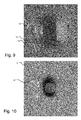
- L2 is different from L1, and on detector 21 the diffracted X-ray beams 17 provide a spot of two-dimensional shape.
- the spot is a two-dimensional projection of the three-dimensional grain morphology and provides information on the shape of the grains boundary.
- the size of the spot increases as the distance L2 increases in comparison to L.
- L2 equals 200% of L the spots correspond to the natural size of the grains, and when L2 is larger than 200% of L a magnification of the spot size occurs. It is preferred that L2 is at least 250% of L such as up to 600% of L.
- the distance L from source 2 to sample 3 is in the range from 5 mm to 200 mm, and the range from 20 mm to 40 mm is preferred.
- the distance L is preferably adjustable in order to adapt the set-up to the specific sample, such as to the size and morphology of the sample.
- this length corresponds to a width of the grain, namely to the calliper width given by the maximum width of the grain along the direction of the lattice planes causing the diffraction.
- the incident X-ray 16 and the diffracted X-ray 17 each forms the Bragg angle ⁇ with a scattering vector 30.
- the scattering vector is orthogonal to the lattice plane, and the incident X-ray 16, the diffracted X-ray 17 and the scattering vector 30 form a common plane.
- the lattice plane 5 has a width along a line 22 orthogonal to said common plane, and the length of the line-shaped segment corresponds to this width.
- the length of the line-shaped segment 13 can thus be used in determining a width of the grain when the grain shape is reconstructed.
- the orientation of the line-shaped segment 13 is directly related to the orientation of the lattice plane 5, and this information can be applied in an indexing process to the model of the three-dimensional grain so that also the crystal orientation is given.
- images obtained with a detector in the second distance L2 can be utilized to provide more details on the actual shape of grain boundaries.
- the individual diffraction event causing a line shape in the first detector position at L1 will in the second detector position at L2 be positioned in the same relative position on the detector, because the deflected X-ray follows a straight line.
- the divergence of the X-ray beam 6 causes the spot to be larger when the distance L2 is larger.
- Each spot is a two-dimensional projection of the three-dimensional grain shape, and the contour of the grain can be determined from the many diffraction events associated with the grain.
- the mapping of grains may also be performed in a forward simulation where an initial three-dimensional model of the polycrystalline material sample is made.
- the outline of the polycrystalline material sample is discretizes into voxels, where each voxel is geometrically smaller than the smallest gain in the material sample.
- the grains are then reconstructed in the model by iterative testing where crystallographic orientations are associated to the voxels, and the diffractions from such orientations are compared with the actually detected line-shaped segments, and the orientations providing matching with the detected line-shaped segments are selected.
- the method uses images acquired with the detector in the first position at the distance L1, and in a segmentation process data on the line-shaped segments are determined and stored in the database.
- the forward simulation process is then performed, involving discretization into voxels, and the three-dimensional geometrical positions of the individual grains are determined, and the crystallographic orientations of the grains are determined.
- the grain shapes may then be further optimized by calculation methods as mentioned, or images acquired at the distance L2 may be used to provide information on the shapes of the grain boundaries.
- Fig. 8 it is also possible to use forward simulation in combination with shape reconstruction, e.g. so that the forward simulation is used to fill out areas of missing or conflicting data.
- FIG. 9 An example of an image detected on the first detector 12 at the distance L1 is shown in Fig. 9 where the line-shaped segments 13 are observed as bright lines 13.
- the second detector 21 need not be located at a position in the direct path of the beam 6.
- the second detector can be located at any position where diffracted signals can be detected.
- the second detector may as an example be located parallel to the first detector, but shifted sideways to be located asymmetrically with respect to the beam 6.
- the second detector need not be parallel to the first detector.
- the second detector may be located as a plane orthogonal to any radius of the length L2 in a sphere having specimen 3 at the centre of the sphere. It is also possible to use several detectors 21 as the second detector.
Landscapes
- Chemical & Material Sciences (AREA)
- Crystallography & Structural Chemistry (AREA)
- Physics & Mathematics (AREA)
- Health & Medical Sciences (AREA)
- Life Sciences & Earth Sciences (AREA)
- Analytical Chemistry (AREA)
- Biochemistry (AREA)
- General Health & Medical Sciences (AREA)
- General Physics & Mathematics (AREA)
- Immunology (AREA)
- Pathology (AREA)
- Analysing Materials By The Use Of Radiation (AREA)
Priority Applications (2)
| Application Number | Priority Date | Filing Date | Title |
|---|---|---|---|
| EP13157864.3A EP2775295B8 (de) | 2013-03-05 | 2013-03-05 | Röntgenstrahlbrechungsverfahren zum Abbilden von Kornstrukturen in einer kristallinen Materialprobe und Röntgenstrahlbrechungsvorrichtung |
| EP14157972.2A EP2775296B1 (de) | 2013-03-05 | 2014-03-05 | Röntgenstrahlbrechungsverfahren zum Abbilden von Kornstrukturen in einer kristallinen Materialprobe und Röntgenstrahlbrechungsvorrichtung |
Applications Claiming Priority (1)
| Application Number | Priority Date | Filing Date | Title |
|---|---|---|---|
| EP13157864.3A EP2775295B8 (de) | 2013-03-05 | 2013-03-05 | Röntgenstrahlbrechungsverfahren zum Abbilden von Kornstrukturen in einer kristallinen Materialprobe und Röntgenstrahlbrechungsvorrichtung |
Publications (3)
| Publication Number | Publication Date |
|---|---|
| EP2775295A1 true EP2775295A1 (de) | 2014-09-10 |
| EP2775295B1 EP2775295B1 (de) | 2016-03-02 |
| EP2775295B8 EP2775295B8 (de) | 2016-05-18 |
Family
ID=47832964
Family Applications (2)
| Application Number | Title | Priority Date | Filing Date |
|---|---|---|---|
| EP13157864.3A Active EP2775295B8 (de) | 2013-03-05 | 2013-03-05 | Röntgenstrahlbrechungsverfahren zum Abbilden von Kornstrukturen in einer kristallinen Materialprobe und Röntgenstrahlbrechungsvorrichtung |
| EP14157972.2A Active EP2775296B1 (de) | 2013-03-05 | 2014-03-05 | Röntgenstrahlbrechungsverfahren zum Abbilden von Kornstrukturen in einer kristallinen Materialprobe und Röntgenstrahlbrechungsvorrichtung |
Family Applications After (1)
| Application Number | Title | Priority Date | Filing Date |
|---|---|---|---|
| EP14157972.2A Active EP2775296B1 (de) | 2013-03-05 | 2014-03-05 | Röntgenstrahlbrechungsverfahren zum Abbilden von Kornstrukturen in einer kristallinen Materialprobe und Röntgenstrahlbrechungsvorrichtung |
Country Status (1)
| Country | Link |
|---|---|
| EP (2) | EP2775295B8 (de) |
Cited By (4)
| Publication number | Priority date | Publication date | Assignee | Title |
|---|---|---|---|---|
| CN110308168A (zh) * | 2018-03-20 | 2019-10-08 | 株式会社理学 | X射线衍射装置 |
| EP3561496A1 (de) * | 2018-04-24 | 2019-10-30 | Rigaku Corporation | Technik zur verarbeitung von röntgenstrahlenbeugungsdaten |
| WO2020051708A1 (en) * | 2018-09-14 | 2020-03-19 | Proto Patents Ltd. | Ball-mapping system and method of operating the same |
| WO2023101800A1 (en) * | 2021-12-01 | 2023-06-08 | Schaeffler Technologies AG & Co. KG | Method of locating poles on bearing elements |
Families Citing this family (1)
| Publication number | Priority date | Publication date | Assignee | Title |
|---|---|---|---|---|
| JP6039093B2 (ja) | 2012-10-18 | 2016-12-07 | カール・ツァイス・エックス−レイ・マイクロスコピー・インコーポレイテッドCarl Zeiss X−Ray Microscopy, Inc. | 結晶学的結晶粒方位マッピング機能を有する実験室x線マイクロトモグラフィシステム |
Citations (3)
| Publication number | Priority date | Publication date | Assignee | Title |
|---|---|---|---|---|
| US3903415A (en) | 1973-03-13 | 1975-09-02 | Max Planck Gesellschaft | X-ray diffraction measurement device using white X-rays |
| US5193104A (en) * | 1990-10-23 | 1993-03-09 | Centre National De La Recherche Scientifique | Method for analyzing monocrystalline parts by x-rays |
| US5491738A (en) | 1993-03-15 | 1996-02-13 | The United States Of America As Represented By The Administrator Of The National Aeronautics And Space Administration | X-ray diffraction apparatus |
Family Cites Families (1)
| Publication number | Priority date | Publication date | Assignee | Title |
|---|---|---|---|---|
| JP6039093B2 (ja) * | 2012-10-18 | 2016-12-07 | カール・ツァイス・エックス−レイ・マイクロスコピー・インコーポレイテッドCarl Zeiss X−Ray Microscopy, Inc. | 結晶学的結晶粒方位マッピング機能を有する実験室x線マイクロトモグラフィシステム |
-
2013
- 2013-03-05 EP EP13157864.3A patent/EP2775295B8/de active Active
-
2014
- 2014-03-05 EP EP14157972.2A patent/EP2775296B1/de active Active
Patent Citations (3)
| Publication number | Priority date | Publication date | Assignee | Title |
|---|---|---|---|---|
| US3903415A (en) | 1973-03-13 | 1975-09-02 | Max Planck Gesellschaft | X-ray diffraction measurement device using white X-rays |
| US5193104A (en) * | 1990-10-23 | 1993-03-09 | Centre National De La Recherche Scientifique | Method for analyzing monocrystalline parts by x-rays |
| US5491738A (en) | 1993-03-15 | 1996-02-13 | The United States Of America As Represented By The Administrator Of The National Aeronautics And Space Administration | X-ray diffraction apparatus |
Non-Patent Citations (7)
| Title |
|---|
| "X-ray diffraction contrast tomography: a novel technique for three-dimensional grain mapping of polycrystals. Part 1: direct beam case", JOURNAL OF APPLIED CRYSTALLOGRAPHY, vol. 41, 2008, pages 302 - 309 |
| HOFMANN F ET AL: "High energy transmission micro-beam Laue synchrotron X-ray diffraction", MATERIALS LETTERS, NORTH HOLLAND PUBLISHING COMPANY. AMSTERDAM, NL, vol. 64, no. 11, 15 June 2010 (2010-06-15), pages 1302 - 1305, XP026995754, ISSN: 0167-577X, [retrieved on 20100310] * |
| LUDWIG W ET AL: "Three-dimensional grain mapping by x-ray diffraction contrast tomography and the use of Friedel pairs in diffraction data analysis", REVIEW OF SCIENTIFIC INSTRUMENTS, AIP, MELVILLE, NY, US, vol. 80, no. 3, 19 March 2009 (2009-03-19), pages 33905 - 33905, XP012128160, ISSN: 0034-6748, DOI: 10.1063/1.3100200 * |
| LYNCH P ET AL: "A laboratory based system for Laue micro x-ray diffraction", REVIEW OF SCIENTIFIC INSTRUMENTS, AIP, MELVILLE, NY, US, vol. 78, no. 2, 9 February 2007 (2007-02-09), pages 23904 - 23904, XP012103777, ISSN: 0034-6748, DOI: 10.1063/1.2437777 * |
| MATTHIAS STOCKMEIER ET AL: "A focusing Laue diffractometer for the investigation of bulk crystals", JOURNAL OF APPLIED CRYSTALLOGRAPHY, vol. 41, no. 4, 1 August 2008 (2008-08-01), pages 754 - 760, XP055059573, ISSN: 0021-8898, DOI: 10.1107/S0021889808012417 * |
| MATTHIAS STOCKMEIER; ANDREAS MAGERL: "A focusing Laue diffractometer for investigation of bulk crystals", JOURNAL OF APPLIED CRYSTALLOGRAPHY, vol. 41, 2008, pages 754 - 760, XP055059573, DOI: doi:10.1107/S0021889808012417 |
| W. LUDWIG ET AL.: "Three-dimensional grain mapping by x-ray diffraction contrast tomography and the use of Friedel pairs in diffraction data analysis", REVIEW OF SCIENTIFIC INSTRUMENTS, vol. 80, 2009, pages 033905 |
Cited By (8)
| Publication number | Priority date | Publication date | Assignee | Title |
|---|---|---|---|---|
| CN110308168A (zh) * | 2018-03-20 | 2019-10-08 | 株式会社理学 | X射线衍射装置 |
| EP3561496A1 (de) * | 2018-04-24 | 2019-10-30 | Rigaku Corporation | Technik zur verarbeitung von röntgenstrahlenbeugungsdaten |
| JP2019203882A (ja) * | 2018-04-24 | 2019-11-28 | 株式会社リガク | X線解析、x線回折データを処理する方法及び装置 |
| US10878615B2 (en) | 2018-04-24 | 2020-12-29 | Rigaku Corporation | Technique for processing X-ray diffraction data |
| JP7205891B2 (ja) | 2018-04-24 | 2023-01-17 | 株式会社リガク | X線解析、x線回折データを処理する方法及び装置 |
| CN110398509B (zh) * | 2018-04-24 | 2024-12-10 | 株式会社理学 | 处理x射线衍射数据的技术 |
| WO2020051708A1 (en) * | 2018-09-14 | 2020-03-19 | Proto Patents Ltd. | Ball-mapping system and method of operating the same |
| WO2023101800A1 (en) * | 2021-12-01 | 2023-06-08 | Schaeffler Technologies AG & Co. KG | Method of locating poles on bearing elements |
Also Published As
| Publication number | Publication date |
|---|---|
| EP2775295B8 (de) | 2016-05-18 |
| EP2775295B1 (de) | 2016-03-02 |
| EP2775296A1 (de) | 2014-09-10 |
| EP2775296B1 (de) | 2018-05-16 |
Similar Documents
| Publication | Publication Date | Title |
|---|---|---|
| US9222901B2 (en) | X-ray diffraction method of mapping grain structures in a crystalline material sample, and an X-ray diffraction apparatus | |
| US9222900B2 (en) | X-ray diffraction method of mapping grain structures in a crystalline material sample, and an X-ray diffraction apparatus | |
| US8477904B2 (en) | X-ray diffraction and computed tomography | |
| US9383324B2 (en) | Laboratory X-ray micro-tomography system with crystallographic grain orientation mapping capabilities | |
| EP2775295B1 (de) | Röntgenstrahlbrechungsverfahren zum Abbilden von Kornstrukturen in einer kristallinen Materialprobe und Röntgenstrahlbrechungsvorrichtung | |
| US11726048B2 (en) | Sample inspection apparatus employing a diffraction detector | |
| EP1978354A1 (de) | Wellenlängendispersive Röntgenfluoreszenzvorrichtung mit energiedispersivem Detektor in Form eines Silicon-drift-detektors zur Verbesserung der Untergrundunterdrückung | |
| EP1653226A1 (de) | Scanzeilendetektor für zweidimensionales Röntgendiffraktometer | |
| US8457280B2 (en) | X-ray diffraction contrast tomography (DCT) system, and X-ray diffraction contrast tomography (DCT) method | |
| EP2896960B1 (de) | Röntgenvorrichtung für SAXS und Bragg-Brentano Messungen | |
| EP1886125B1 (de) | Zweidimensionale kleinwinkel-röntgenstreuungskamera | |
| EP3809123A1 (de) | Schnelle industrielle computertomographie für grosse objekte | |
| GB2560165A (en) | Sample inspection apparatus employing a diffraction detector | |
| US12209978B2 (en) | Laboratory-based 3D scanning X-ray Laue micro-diffraction system and method (Lab3DμXRD) | |
| GB2560163A (en) | Sample inspection apparatus employing a diffraction detector | |
| EP2365319B1 (de) | Röntgenstrahldiffraktion und computergesteuerte Tomografie | |
| GB2560696A (en) | Sample inspection apparatus employing a diffraction detector | |
| CN110779940A (zh) | 发散束二维x射线衍射 | |
| Pella | Blaj (45) Date of Patent: Jul. 2, 2013 |
Legal Events
| Date | Code | Title | Description |
|---|---|---|---|
| PUAI | Public reference made under article 153(3) epc to a published international application that has entered the european phase |
Free format text: ORIGINAL CODE: 0009012 |
|
| 17P | Request for examination filed |
Effective date: 20130305 |
|
| AK | Designated contracting states |
Kind code of ref document: A1 Designated state(s): AL AT BE BG CH CY CZ DE DK EE ES FI FR GB GR HR HU IE IS IT LI LT LU LV MC MK MT NL NO PL PT RO RS SE SI SK SM TR |
|
| AX | Request for extension of the european patent |
Extension state: BA ME |
|
| R17P | Request for examination filed (corrected) |
Effective date: 20150309 |
|
| RBV | Designated contracting states (corrected) |
Designated state(s): AL AT BE BG CH CY CZ DE DK EE ES FI FR GB GR HR HU IE IS IT LI LT LU LV MC MK MT NL NO PL PT RO RS SE SI SK SM TR |
|
| REG | Reference to a national code |
Ref country code: DE Ref legal event code: R079 Ref document number: 602013005204 Country of ref document: DE Free format text: PREVIOUS MAIN CLASS: G01N0023200000 Ipc: G01N0023207000 |
|
| GRAP | Despatch of communication of intention to grant a patent |
Free format text: ORIGINAL CODE: EPIDOSNIGR1 |
|
| RIC1 | Information provided on ipc code assigned before grant |
Ipc: G01N 23/207 20060101AFI20150716BHEP |
|
| INTG | Intention to grant announced |
Effective date: 20150817 |
|
| GRAS | Grant fee paid |
Free format text: ORIGINAL CODE: EPIDOSNIGR3 |
|
| GRAA | (expected) grant |
Free format text: ORIGINAL CODE: 0009210 |
|
| AK | Designated contracting states |
Kind code of ref document: B1 Designated state(s): AL AT BE BG CH CY CZ DE DK EE ES FI FR GB GR HR HU IE IS IT LI LT LU LV MC MK MT NL NO PL PT RO RS SE SI SK SM TR |
|
| REG | Reference to a national code |
Ref country code: GB Ref legal event code: FG4D |
|
| REG | Reference to a national code |
Ref country code: AT Ref legal event code: REF Ref document number: 778389 Country of ref document: AT Kind code of ref document: T Effective date: 20160315 Ref country code: CH Ref legal event code: EP |
|
| REG | Reference to a national code |
Ref country code: IE Ref legal event code: FG4D |
|
| REG | Reference to a national code |
Ref country code: DE Ref legal event code: R096 Ref document number: 602013005204 Country of ref document: DE |
|
| RIN2 | Information on inventor provided after grant (corrected) |
Inventor name: HOLZNER, CHRISTIAN Inventor name: LAURIDSEN, ERIK Inventor name: FESER, MICHAEL Inventor name: POULSEN, STEFAN OTHMAR |
|
| REG | Reference to a national code |
Ref country code: FR Ref legal event code: PLFP Year of fee payment: 4 |
|
| REG | Reference to a national code |
Ref country code: NL Ref legal event code: MP Effective date: 20160302 |
|
| REG | Reference to a national code |
Ref country code: LT Ref legal event code: MG4D |
|
| REG | Reference to a national code |
Ref country code: AT Ref legal event code: MK05 Ref document number: 778389 Country of ref document: AT Kind code of ref document: T Effective date: 20160302 |
|
| PG25 | Lapsed in a contracting state [announced via postgrant information from national office to epo] |
Ref country code: GR Free format text: LAPSE BECAUSE OF FAILURE TO SUBMIT A TRANSLATION OF THE DESCRIPTION OR TO PAY THE FEE WITHIN THE PRESCRIBED TIME-LIMIT Effective date: 20160603 Ref country code: FI Free format text: LAPSE BECAUSE OF FAILURE TO SUBMIT A TRANSLATION OF THE DESCRIPTION OR TO PAY THE FEE WITHIN THE PRESCRIBED TIME-LIMIT Effective date: 20160302 Ref country code: HR Free format text: LAPSE BECAUSE OF FAILURE TO SUBMIT A TRANSLATION OF THE DESCRIPTION OR TO PAY THE FEE WITHIN THE PRESCRIBED TIME-LIMIT Effective date: 20160302 Ref country code: NO Free format text: LAPSE BECAUSE OF FAILURE TO SUBMIT A TRANSLATION OF THE DESCRIPTION OR TO PAY THE FEE WITHIN THE PRESCRIBED TIME-LIMIT Effective date: 20160602 Ref country code: ES Free format text: LAPSE BECAUSE OF FAILURE TO SUBMIT A TRANSLATION OF THE DESCRIPTION OR TO PAY THE FEE WITHIN THE PRESCRIBED TIME-LIMIT Effective date: 20160302 |
|
| PG25 | Lapsed in a contracting state [announced via postgrant information from national office to epo] |
Ref country code: SE Free format text: LAPSE BECAUSE OF FAILURE TO SUBMIT A TRANSLATION OF THE DESCRIPTION OR TO PAY THE FEE WITHIN THE PRESCRIBED TIME-LIMIT Effective date: 20160302 Ref country code: LT Free format text: LAPSE BECAUSE OF FAILURE TO SUBMIT A TRANSLATION OF THE DESCRIPTION OR TO PAY THE FEE WITHIN THE PRESCRIBED TIME-LIMIT Effective date: 20160302 Ref country code: RS Free format text: LAPSE BECAUSE OF FAILURE TO SUBMIT A TRANSLATION OF THE DESCRIPTION OR TO PAY THE FEE WITHIN THE PRESCRIBED TIME-LIMIT Effective date: 20160302 Ref country code: BE Free format text: LAPSE BECAUSE OF NON-PAYMENT OF DUE FEES Effective date: 20160331 Ref country code: NL Free format text: LAPSE BECAUSE OF FAILURE TO SUBMIT A TRANSLATION OF THE DESCRIPTION OR TO PAY THE FEE WITHIN THE PRESCRIBED TIME-LIMIT Effective date: 20160302 Ref country code: AT Free format text: LAPSE BECAUSE OF FAILURE TO SUBMIT A TRANSLATION OF THE DESCRIPTION OR TO PAY THE FEE WITHIN THE PRESCRIBED TIME-LIMIT Effective date: 20160302 Ref country code: LV Free format text: LAPSE BECAUSE OF FAILURE TO SUBMIT A TRANSLATION OF THE DESCRIPTION OR TO PAY THE FEE WITHIN THE PRESCRIBED TIME-LIMIT Effective date: 20160302 Ref country code: PL Free format text: LAPSE BECAUSE OF FAILURE TO SUBMIT A TRANSLATION OF THE DESCRIPTION OR TO PAY THE FEE WITHIN THE PRESCRIBED TIME-LIMIT Effective date: 20160302 |
|
| PG25 | Lapsed in a contracting state [announced via postgrant information from national office to epo] |
Ref country code: IS Free format text: LAPSE BECAUSE OF FAILURE TO SUBMIT A TRANSLATION OF THE DESCRIPTION OR TO PAY THE FEE WITHIN THE PRESCRIBED TIME-LIMIT Effective date: 20160702 Ref country code: EE Free format text: LAPSE BECAUSE OF FAILURE TO SUBMIT A TRANSLATION OF THE DESCRIPTION OR TO PAY THE FEE WITHIN THE PRESCRIBED TIME-LIMIT Effective date: 20160302 |
|
| REG | Reference to a national code |
Ref country code: CH Ref legal event code: PL |
|
| PG25 | Lapsed in a contracting state [announced via postgrant information from national office to epo] |
Ref country code: CZ Free format text: LAPSE BECAUSE OF FAILURE TO SUBMIT A TRANSLATION OF THE DESCRIPTION OR TO PAY THE FEE WITHIN THE PRESCRIBED TIME-LIMIT Effective date: 20160302 Ref country code: SK Free format text: LAPSE BECAUSE OF FAILURE TO SUBMIT A TRANSLATION OF THE DESCRIPTION OR TO PAY THE FEE WITHIN THE PRESCRIBED TIME-LIMIT Effective date: 20160302 Ref country code: RO Free format text: LAPSE BECAUSE OF FAILURE TO SUBMIT A TRANSLATION OF THE DESCRIPTION OR TO PAY THE FEE WITHIN THE PRESCRIBED TIME-LIMIT Effective date: 20160302 Ref country code: PT Free format text: LAPSE BECAUSE OF FAILURE TO SUBMIT A TRANSLATION OF THE DESCRIPTION OR TO PAY THE FEE WITHIN THE PRESCRIBED TIME-LIMIT Effective date: 20160704 Ref country code: SM Free format text: LAPSE BECAUSE OF FAILURE TO SUBMIT A TRANSLATION OF THE DESCRIPTION OR TO PAY THE FEE WITHIN THE PRESCRIBED TIME-LIMIT Effective date: 20160302 |
|
| REG | Reference to a national code |
Ref country code: DE Ref legal event code: R097 Ref document number: 602013005204 Country of ref document: DE |
|
| REG | Reference to a national code |
Ref country code: IE Ref legal event code: MM4A |
|
| PG25 | Lapsed in a contracting state [announced via postgrant information from national office to epo] |
Ref country code: BE Free format text: LAPSE BECAUSE OF FAILURE TO SUBMIT A TRANSLATION OF THE DESCRIPTION OR TO PAY THE FEE WITHIN THE PRESCRIBED TIME-LIMIT Effective date: 20160302 Ref country code: IT Free format text: LAPSE BECAUSE OF FAILURE TO SUBMIT A TRANSLATION OF THE DESCRIPTION OR TO PAY THE FEE WITHIN THE PRESCRIBED TIME-LIMIT Effective date: 20160302 |
|
| PLBE | No opposition filed within time limit |
Free format text: ORIGINAL CODE: 0009261 |
|
| STAA | Information on the status of an ep patent application or granted ep patent |
Free format text: STATUS: NO OPPOSITION FILED WITHIN TIME LIMIT |
|
| PG25 | Lapsed in a contracting state [announced via postgrant information from national office to epo] |
Ref country code: CH Free format text: LAPSE BECAUSE OF NON-PAYMENT OF DUE FEES Effective date: 20160331 Ref country code: DK Free format text: LAPSE BECAUSE OF FAILURE TO SUBMIT A TRANSLATION OF THE DESCRIPTION OR TO PAY THE FEE WITHIN THE PRESCRIBED TIME-LIMIT Effective date: 20160302 Ref country code: IE Free format text: LAPSE BECAUSE OF NON-PAYMENT OF DUE FEES Effective date: 20160305 Ref country code: LI Free format text: LAPSE BECAUSE OF NON-PAYMENT OF DUE FEES Effective date: 20160331 |
|
| 26N | No opposition filed |
Effective date: 20161205 |
|
| PG25 | Lapsed in a contracting state [announced via postgrant information from national office to epo] |
Ref country code: SI Free format text: LAPSE BECAUSE OF FAILURE TO SUBMIT A TRANSLATION OF THE DESCRIPTION OR TO PAY THE FEE WITHIN THE PRESCRIBED TIME-LIMIT Effective date: 20160302 Ref country code: BG Free format text: LAPSE BECAUSE OF FAILURE TO SUBMIT A TRANSLATION OF THE DESCRIPTION OR TO PAY THE FEE WITHIN THE PRESCRIBED TIME-LIMIT Effective date: 20160602 |
|
| REG | Reference to a national code |
Ref country code: FR Ref legal event code: PLFP Year of fee payment: 5 |
|
| PG25 | Lapsed in a contracting state [announced via postgrant information from national office to epo] |
Ref country code: MT Free format text: LAPSE BECAUSE OF FAILURE TO SUBMIT A TRANSLATION OF THE DESCRIPTION OR TO PAY THE FEE WITHIN THE PRESCRIBED TIME-LIMIT Effective date: 20160302 |
|
| REG | Reference to a national code |
Ref country code: DE Ref legal event code: R081 Ref document number: 602013005204 Country of ref document: DE Owner name: XNOVO TECHNOLOGY APS, DK Free format text: FORMER OWNER: DANMARKS TEKNISKE UNIVERSITET, LYNGBY, DK |
|
| REG | Reference to a national code |
Ref country code: GB Ref legal event code: 732E Free format text: REGISTERED BETWEEN 20171005 AND 20171011 |
|
| REG | Reference to a national code |
Ref country code: FR Ref legal event code: TP Owner name: XNOVO TECHNOLOGY APS, DK Effective date: 20171226 |
|
| REG | Reference to a national code |
Ref country code: FR Ref legal event code: PLFP Year of fee payment: 6 |
|
| PG25 | Lapsed in a contracting state [announced via postgrant information from national office to epo] |
Ref country code: HU Free format text: LAPSE BECAUSE OF FAILURE TO SUBMIT A TRANSLATION OF THE DESCRIPTION OR TO PAY THE FEE WITHIN THE PRESCRIBED TIME-LIMIT; INVALID AB INITIO Effective date: 20130305 |
|
| PG25 | Lapsed in a contracting state [announced via postgrant information from national office to epo] |
Ref country code: TR Free format text: LAPSE BECAUSE OF FAILURE TO SUBMIT A TRANSLATION OF THE DESCRIPTION OR TO PAY THE FEE WITHIN THE PRESCRIBED TIME-LIMIT Effective date: 20160302 Ref country code: LU Free format text: LAPSE BECAUSE OF NON-PAYMENT OF DUE FEES Effective date: 20160305 Ref country code: MC Free format text: LAPSE BECAUSE OF FAILURE TO SUBMIT A TRANSLATION OF THE DESCRIPTION OR TO PAY THE FEE WITHIN THE PRESCRIBED TIME-LIMIT Effective date: 20160302 Ref country code: CY Free format text: LAPSE BECAUSE OF FAILURE TO SUBMIT A TRANSLATION OF THE DESCRIPTION OR TO PAY THE FEE WITHIN THE PRESCRIBED TIME-LIMIT Effective date: 20160302 Ref country code: MK Free format text: LAPSE BECAUSE OF FAILURE TO SUBMIT A TRANSLATION OF THE DESCRIPTION OR TO PAY THE FEE WITHIN THE PRESCRIBED TIME-LIMIT Effective date: 20160302 Ref country code: MT Free format text: LAPSE BECAUSE OF FAILURE TO SUBMIT A TRANSLATION OF THE DESCRIPTION OR TO PAY THE FEE WITHIN THE PRESCRIBED TIME-LIMIT Effective date: 20160331 |
|
| PG25 | Lapsed in a contracting state [announced via postgrant information from national office to epo] |
Ref country code: AL Free format text: LAPSE BECAUSE OF FAILURE TO SUBMIT A TRANSLATION OF THE DESCRIPTION OR TO PAY THE FEE WITHIN THE PRESCRIBED TIME-LIMIT Effective date: 20160302 |
|
| PGFP | Annual fee paid to national office [announced via postgrant information from national office to epo] |
Ref country code: DE Payment date: 20250416 Year of fee payment: 13 |
|
| PGFP | Annual fee paid to national office [announced via postgrant information from national office to epo] |
Ref country code: GB Payment date: 20260327 Year of fee payment: 14 |
|
| PGFP | Annual fee paid to national office [announced via postgrant information from national office to epo] |
Ref country code: FR Payment date: 20260317 Year of fee payment: 14 |