EP2775329B1 - Laser accordable avec structure de réseau de Bragg - Google Patents
Laser accordable avec structure de réseau de Bragg Download PDFInfo
- Publication number
- EP2775329B1 EP2775329B1 EP14166112.4A EP14166112A EP2775329B1 EP 2775329 B1 EP2775329 B1 EP 2775329B1 EP 14166112 A EP14166112 A EP 14166112A EP 2775329 B1 EP2775329 B1 EP 2775329B1
- Authority
- EP
- European Patent Office
- Prior art keywords
- grating
- wavelength
- tunable laser
- envelope function
- gain
- Prior art date
- Legal status (The legal status is an assumption and is not a legal conclusion. Google has not performed a legal analysis and makes no representation as to the accuracy of the status listed.)
- Active
Links
Images


Classifications
-
- H—ELECTRICITY
- H01—ELECTRIC ELEMENTS
- H01S—DEVICES USING THE PROCESS OF LIGHT AMPLIFICATION BY STIMULATED EMISSION OF RADIATION [LASER] TO AMPLIFY OR GENERATE LIGHT; DEVICES USING STIMULATED EMISSION OF ELECTROMAGNETIC RADIATION IN WAVE RANGES OTHER THAN OPTICAL
- H01S5/00—Semiconductor lasers
- H01S5/06—Arrangements for controlling the laser output parameters, e.g. by operating on the active medium
- H01S5/062—Arrangements for controlling the laser output parameters, e.g. by operating on the active medium by varying the potential of the electrodes
- H01S5/0625—Arrangements for controlling the laser output parameters, e.g. by operating on the active medium by varying the potential of the electrodes in multi-section lasers
- H01S5/06255—Controlling the frequency of the radiation
- H01S5/06256—Controlling the frequency of the radiation with DBR-structure
-
- G—PHYSICS
- G02—OPTICS
- G02B—OPTICAL ELEMENTS, SYSTEMS OR APPARATUS
- G02B5/00—Optical elements other than lenses
- G02B5/18—Diffraction gratings
- G02B5/1861—Reflection gratings characterised by their structure, e.g. step profile, contours of substrate or grooves, pitch variations, materials
-
- H—ELECTRICITY
- H01—ELECTRIC ELEMENTS
- H01S—DEVICES USING THE PROCESS OF LIGHT AMPLIFICATION BY STIMULATED EMISSION OF RADIATION [LASER] TO AMPLIFY OR GENERATE LIGHT; DEVICES USING STIMULATED EMISSION OF ELECTROMAGNETIC RADIATION IN WAVE RANGES OTHER THAN OPTICAL
- H01S3/00—Lasers, i.e. devices using stimulated emission of electromagnetic radiation in the infrared, visible or ultraviolet wave range
- H01S3/05—Construction or shape of optical resonators; Accommodation of active medium therein; Shape of active medium
- H01S3/08—Construction or shape of optical resonators or components thereof
- H01S3/08004—Construction or shape of optical resonators or components thereof incorporating a dispersive element, e.g. a prism for wavelength selection
- H01S3/08009—Construction or shape of optical resonators or components thereof incorporating a dispersive element, e.g. a prism for wavelength selection using a diffraction grating
-
- H—ELECTRICITY
- H01—ELECTRIC ELEMENTS
- H01S—DEVICES USING THE PROCESS OF LIGHT AMPLIFICATION BY STIMULATED EMISSION OF RADIATION [LASER] TO AMPLIFY OR GENERATE LIGHT; DEVICES USING STIMULATED EMISSION OF ELECTROMAGNETIC RADIATION IN WAVE RANGES OTHER THAN OPTICAL
- H01S3/00—Lasers, i.e. devices using stimulated emission of electromagnetic radiation in the infrared, visible or ultraviolet wave range
- H01S3/10—Controlling the intensity, frequency, phase, polarisation or direction of the emitted radiation, e.g. switching, gating, modulating or demodulating
-
- H—ELECTRICITY
- H01—ELECTRIC ELEMENTS
- H01S—DEVICES USING THE PROCESS OF LIGHT AMPLIFICATION BY STIMULATED EMISSION OF RADIATION [LASER] TO AMPLIFY OR GENERATE LIGHT; DEVICES USING STIMULATED EMISSION OF ELECTROMAGNETIC RADIATION IN WAVE RANGES OTHER THAN OPTICAL
- H01S5/00—Semiconductor lasers
- H01S5/10—Construction or shape of the optical resonator, e.g. extended or external cavity, coupled cavities, bent-guide, varying width, thickness or composition of the active region
- H01S5/12—Construction or shape of the optical resonator, e.g. extended or external cavity, coupled cavities, bent-guide, varying width, thickness or composition of the active region the resonator having a periodic structure, e.g. in distributed feedback [DFB] lasers
- H01S5/125—Distributed Bragg reflector [DBR] lasers
-
- H—ELECTRICITY
- H01—ELECTRIC ELEMENTS
- H01S—DEVICES USING THE PROCESS OF LIGHT AMPLIFICATION BY STIMULATED EMISSION OF RADIATION [LASER] TO AMPLIFY OR GENERATE LIGHT; DEVICES USING STIMULATED EMISSION OF ELECTROMAGNETIC RADIATION IN WAVE RANGES OTHER THAN OPTICAL
- H01S5/00—Semiconductor lasers
- H01S5/10—Construction or shape of the optical resonator, e.g. extended or external cavity, coupled cavities, bent-guide, varying width, thickness or composition of the active region
- H01S5/12—Construction or shape of the optical resonator, e.g. extended or external cavity, coupled cavities, bent-guide, varying width, thickness or composition of the active region the resonator having a periodic structure, e.g. in distributed feedback [DFB] lasers
- H01S5/1206—Construction or shape of the optical resonator, e.g. extended or external cavity, coupled cavities, bent-guide, varying width, thickness or composition of the active region the resonator having a periodic structure, e.g. in distributed feedback [DFB] lasers having a non constant or multiplicity of periods
- H01S5/1209—Sampled grating
-
- H—ELECTRICITY
- H01—ELECTRIC ELEMENTS
- H01S—DEVICES USING THE PROCESS OF LIGHT AMPLIFICATION BY STIMULATED EMISSION OF RADIATION [LASER] TO AMPLIFY OR GENERATE LIGHT; DEVICES USING STIMULATED EMISSION OF ELECTROMAGNETIC RADIATION IN WAVE RANGES OTHER THAN OPTICAL
- H01S5/00—Semiconductor lasers
- H01S5/10—Construction or shape of the optical resonator, e.g. extended or external cavity, coupled cavities, bent-guide, varying width, thickness or composition of the active region
- H01S5/12—Construction or shape of the optical resonator, e.g. extended or external cavity, coupled cavities, bent-guide, varying width, thickness or composition of the active region the resonator having a periodic structure, e.g. in distributed feedback [DFB] lasers
- H01S5/1206—Construction or shape of the optical resonator, e.g. extended or external cavity, coupled cavities, bent-guide, varying width, thickness or composition of the active region the resonator having a periodic structure, e.g. in distributed feedback [DFB] lasers having a non constant or multiplicity of periods
- H01S5/1212—Chirped grating
Definitions
- the present invention relates to a tunable laser comprising a Bragg grating structure.
- the invention relates to a tunable laser comprising a modified Bragg grating structure to facilitate the production of a level modal gain.
- optical and optical are used in this specification in a non-specific sense, that is so as to cover use with radiation in the visible and non-visible parts of the spectrum, and so as not to be limited to use with visible light.
- light may apply to electromagnetic radiation of any frequency, and is not limited to light in the visible spectrum.
- waveguide describes a structure that guides light and which may comprise a plurality of layers.
- Tunable lasers are important for a number of applications in optical telecommunications and signal processing applications.
- the design and operation of tunable lasers is described, for example, in the article " Tunable Laser Diodes” by Markus-Christian Amann and Jens Buus (ISBN 0890069638 ).
- An exemplary design of tunable laser comprises a gain region bounded at one end by a reflector in the form of a Distributed Bragg Reflector (DBR) adapted to reflect a range of wavelengths (often known as a chirped grating), and at the other end by a DBR adapted to reflect a "comb" spectrum of discrete wavelength peaks.
- DBR Distributed Bragg Reflector
- US 5838714 describes a three section DBR laser in which the DBR is segmented and composed of a repeating chirped pattern, with interdigitated electrodes connected such that each segment of grating is electrically connected in parallel with all other comparable sections.
- each segment of grating is electrically connected in parallel with all other comparable sections.
- US 5379318 describes a tunable laser in which two segmented DBRs, one on either side of a gain section, are used that each produce a comb-like reflection spectrum, and the two spectra have interleaved peaks, such that an individual peak from one segment can be tuned to overlap that of a peak in the other DBR, in order to create and define an optical cavity that is above the lasing threshold.
- FBGs Fibre Bragg Gratings
- DBRs distributed Bragg Reflectors
- a Bragg grating comprises a periodic modulation of the refractive index of a waveguide. Light is scattered at each change in refractive index. If the Bragg condition is satisfied, the light reflected at each of the grating planes interferes constructively.
- a grating of constant pitch and reflective strength thus produces a reflection of light of a wavelength of twice the effective pitch of the grating, where the effective pitch differs from actual pitch by a factor of n eff .
- the grating is typically formed by etching a lithographic pattern in a chemical resist into the structure, part of the way through epitaxial growth, and then overgrowing with a material of different refractive index.
- the lithographic patterns may be written holographically using an optical interference pattern, photolithographically by exposing through a mask onto a light sensitive resist (photoresist), or by electron-beam (“e-beam”) lithography using e-beam sensitive resist.
- Bragg gratings can also be adapted to reflect a range of wavelengths, and these are known as chirped gratings.
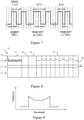
- the pitch A of a chirped grating varies along the length of the grating, commonly monotonically, as shown schematically in Figure 1 .
- a chirped grating of constant reflective strength should produce a reflection spectrum (reflectivity plotted against wavelength) in the shape of a "top hat", i.e. the reflection of the grating is substantially uniform within a specific wavelength range, as shown in Figure 2 .
- Chirped gratings are often incorporated into tunable semiconductor lasers as a reflector at one end of the gain region of the laser, and an example is shown in WO 03/012936 . Further examples may be seen in US 6771687 , which provides an example of how FBGs may be used in an FBG stabilised laser, and US 6345135 , which illustrates applications of DBRs in semiconductor optoelectronic devices.
- the reflector at the other end of a tunable laser may be arranged to produce a "comb" of reflective peaks at discrete wavelengths, as shown in Figure 3 .
- This comb-like spectrum can be produced by a segmented grating with a stepped pitch - i.e. a series of discrete grating segments, each of different pitches.
- comb grating An alternative form of comb grating is known as a "sampled grating" and an example is shown schematically in Figure 4 .
- the DBR comprises a repeating pattern of units 1, 2, 3, each unit comprising a constant pitch grating 4, 5, 6 followed by a region 7, 8, 9 from which the grating is absent. Sampled gratings are described, for example, in Amman and Buus (ISBN 0890069638 - mentioned above) and US 6141370 .
- the grating-less regions 7, 8, 9 are much greater in length than the grating period ⁇ 1 .
- DBRs of this form produce a comb of reflection peaks with a sinc 2 envelope function, i.e.
- the envelope function is peaked at a central maximum, falling away at the sides, such that reflective peaks away from the centre of the operating range typically have a weaker reflection, as shown in Figure 5 .
- the shape of these DBRs makes it difficult to operate two of them together with different peak spacings in a Vernier manner, as described in US 4896325 .
- the sampled grating can be modified to produce a flat topped comb-like reflector (as shown in Figure 3 ) by replacing the constant pitch gratings in each unit by chirped gratings, as described in US 5325392 and US 6141370 .
- Such gratings are known as "superstructure gratings” or “periodically chirped gratings”. More complex non-binary superstructure gratings are also known.
- phase change grating Another DBR that produces a comb-like reflection spectrum is known as a "phase change grating" and an example is shown in Figure 6 .
- Such a grating typically comprises sections of constant pitch grating 10-15 separated by phase changes 16 of ⁇ radians, and by careful design can produce a comb of reflection peaks within a substantially flat topped envelope function, as explained in US 6345135 .
- Such gratings require complex computer modelling and optimisation, and are considered to be particularly sensitive to design variations.
- a further DBR for producing a comb-like structure is known as a "superimposed grating" and an example is shown in Figure 7 and described in US 3141370 .
- DBRs for use in tunable lasers are generally designed to produce one of three types of reflection spectrum: the "top hat" of Figure 2 produced by a chirped grating; the comb of Figure 3 with uniform peak heights produced by some stepped segmented gratings and phase change gratings; and the comb modulated by a sine 2 function of Figure 5 produced by a sampled grating.
- the light produced by the active medium in the gain section of a semiconductor laser exhibits a characteristic spectral profile that is usually peaked, and the materials of the laser are typically chosen such that the peak lies within the operating range of the laser.
- this peaked shape is disadvantageous in a tunable laser when it is operated away from the wavelength of the peak.
- the shape of the gain band is usually roughly parabolic, and the gain is reduced at the highest and lowest wavelengths.
- the usable tuning range of the laser is thus limited by the low gain at these wavelengths. It has in the past been attempted to overcome this problem by altering the active medium to "flatten" the gain band but implementation of this is difficult.
- EP 0955558 describes a multi-wavelength optical reflector which includes a diffraction grating structure and a tunable laser comprising diffraction grating structures having a plurality of repeat grating units in which each grating unit comprises a series of adjacent diffraction gratings having the same pitch, characterised in that grating units and adjacent gratings within a grating unit are separated by a phase change of substantially pi (n) radians and wherein at least two of the gratings within a grating unit have different lengths, the lengths being selected so as to provide a predetermined reflection spectrum.
- a chirped Bragg grating having a local reflection strength which varies with position along the length of the grating so as to generate an overall reflection strength spectrum which is non-uniform with respect to wavelength between two wavelength extremities.
- the non-uniform reflection strength of the chirped Bragg grating may then be used to compensate for the non-uniform shape of the gain profile of the gain section of a tunable laser, or for other optical cavity losses.
- a typical chirped grating comprises a periodic pattern of marks and spaces whose period varies along the length of the grating.
- the grating may comprise one or more reduced reflective strength regions, each formed by the base order periodic pattern of marks and spaces from which at least some of the marks are missing. This enables the local reflective strength to be controlled without the need to change the grating amplitude or the mark:space ratio, which is a particularly useful feature for gratings manufactured by e-beam lithography.
- the pattern in each of the reduced reflective strength regions is preferably defined by the base order pattern modulated by a higher order envelope function that determines which marks are missing from the base order pattern.
- the local reflection strength along the length of the grating may be varied by changing the mark width: space width ratio along the length of the grating, or by varying the difference in refractive index between marks and spaces.
- the reflection strength of the grating is higher for wavelengths at the extremities of the reflection spectrum than for wavelengths between these extremities. This enables the grating to be used to compensate for the parabolic gain profile typically found in the gain section of tunable semiconductor lasers.
- the reflection spectrum may have a "dished" profile, which may be symmetric or asymmetric.
- the reflection strength of the grating may increase, possibly linearly, from one wavelength extremity to the other wavelength extremity.
- the "dished" profile may be combined with an underlying rising trend between the wavelength extremities.
- a tunable laser in accordance with claim 1. Further aspects and preferred embodiments are set out in claim 2 et seq.
- a comb grating having a non-uniform reflection spectrum may be used instead of (or in addition to) a chirped grating to compensate for the non-uniform shape of the gain profile of the gain section.
- the optimisation of section lengths enables other envelope functions to be chosen if necessary, to compensate for different shapes of gain profile or optical cavity losses.
- Each phase change between sections may be of ⁇ radians.
- the envelope function may be asymmetric, and this is preferably achieved by choosing the position and size of the phase changes between grating sections to control the asymmetry of the envelope function.
- the phase changes are preferably different from ⁇ radians.
- a Bragg grating may be adapted to produce a reflection spectrum comprising a comb of reflective peaks at discrete wavelengths, the peaks having reflection amplitudes modulated by an envelope function, the grating comprising a plurality of periodic grating sections, each having a different pitch, wherein the relative reflective strength of the grating sections is varied with position along the length of the grating to control the envelope function.
- the envelope function of the reflection spectrum is preferably higher at the wavelength extremities than between these extremities.
- a tunable laser comprising a gain section bounded at each end by a reflector, the gain section having a non-uniform wavelength gain profile, wherein at least one of the reflectors is a Bragg grating as described above.
- the reflection spectrum of the grating has an amplitude envelope function adapted to vary with wavelength in an opposite fashion to the gain profile so as to compensate at least partially for the non-uniform gain profile.
- the reflection spectrum of the at least one reflector preferably exhibits higher reflection at the wavelength extremities than between these extremities so as to compensate for a gain profile higher in the middle than at the edges.
- One of the reflectors may be a chirped reflector adapted to reflect a continuous range of wavelengths.
- the other reflector may be a comb reflector adapted to produce a comb of reflective peaks, and the comb reflector may be adapted instead of (or as well as) the chirped reflector as the compensating reflector.
- both reflectors are comb reflectors adapted to reflect a range of reflective peaks.
- either or both comb reflectors may be used to compensate for the non-uniform gain profile.
- a method of manufacturing a chirped Bragg grating having a non-uniform wavelength reflection spectrum comprising varying the reflection strength along the length of the grating.
- FIG 8 is a schematic representation of a typical tunable laser 20, of the type described in WO 03/012936 .
- the laser is built up in a series of layers, with a waveguide layer 21 bounded by a lower layer 22 and upper layer 23.
- the structure may include further layers, but they are not material to the invention and are not shown for clarity.
- the laser 20 has four principal sections: a gain section 24, a phase change section 25 and front and rear reflecting sections 26, 27.
- the rear reflecting section 27 has a phase change grating distributed Bragg reflector 28 (similar to that shown in Figure 6 ) formed in the upper layer 23. This reflector produces a comb of reflectance peaks at separated wavelengths.
- the front reflecting section 26 consists of a linearly chirped grating 29 of progressive pitch variation along the length. It will be noted that the chirped reflector of Figure 8 is represented as a sinusoidal variation in refractive index, whereas the chirped reflector previously shown in Figure 1 is castellated. The physical shape depends largely on the manufacturing method used to produce the grating. Both types of grating work in a similar manner and for the present invention may be considered to be interchangeable.
- the laser operates by injecting sufficient current into the gain section 24 to create a population inversion of charge carriers, and by making a portion of the front grating 26 reflect light of a specific wavelength preferentially, so that the rear grating 27 selectively reflects light of that particular wavelength.
- the front grating will reflect back the light at that wavelength, so that the wavelength will become the preferred or enhanced wavelength and the laser will start to lase at that wavelength.
- the mechanism by which a preferred wavelength is selected is well known and described, for example, in WO 03/012936 and will not be reproduced here.
- the gain section 24 can support lasing at a range of wavelengths, but does not provide uniform gain across that range.
- a gain section in a typical tunable laser has a gain wavelength profile which is approximately parabolic, with a maximum within the operating wavelength range of the tunable laser. At the edges of the gain profile the gain falls off until it is too low for lasing, and this limits the useful tunable operating range of the laser.
- one or both of the reflectors 26, 27 are provided with a "dished" reflection spectrum, so that the reflectivity at the ends of the range is higher than between these ends, as shown in Figure 9 .
- Either the chirped grating 29 or the phase change grating 28 (or both) may be dished in this manner and each is discussed in turn.
- Such dishing has the technical advantages of enhancing performance of lasing modes at the extremities of the tuning range and producing a flatter power spectrum for a fixed gain current or a reduction in the gain current budget of the tunable laser.
- a monotonically chirped grating can be given a dished reflection spectrum by producing a non-uniform local reflection strength along the length of the grating, such that the grating region of intermediate pitch is of lower reflection strength than the extremities of the range of pitches.
- the reflection strength in the central region can be reduced in a number of different ways.
- the relative height of the refractive index peaks and troughs may be reduced.
- the mark:space ratio may be changed.
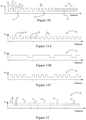
- An example of a dished chirped grating of this type is shown in Figure 10 .
- the grating 30 comprises a series of spaces 31 and marks 32 with higher refractive index.
- the grating is divided into regions 33, 34, 35 having decreasing pitch ⁇ 33 , ⁇ 34 , ⁇ 35 . In the end regions 33, 35, the widths of the marks and spaces are approximately equal ( i.e. the mark:space ratio ⁇ 1).
- the marks 32 are substantially narrower than the spaces 31 (i .e. the mark:space ratio ⁇ 0.25).
- the reflective strength of a section of grating is controlled by the mark:space ratio, and for a first order grating is higher when this ratio is close to 1.
- the reflective strength of the central region 34 (and thus the central wavelengths) is lower than for the outer regions 33, 35 (and thus the outer wavelengths).
- the grating 30 shown in Figure 10 will have a reflection spectrum similar to that shown in Figure 9 .
- mark:space ratio There are occasions where variation in mark:space ratio is not desirable. Away from a mark:space ratio of 1 (for a first order grating) it can be difficult to manufacture the grating and it may be vulnerable to manufacturing variations. In such situations it may be desirable to reduce the strength of portions of a grating using a "deleted marks" approach. This approach is particularly suitable for gratings written by e-beam lithography and is described in detail in British patent no. 2418995 . A brief explanation is also given with reference to Figures 11A to 11C .
- Figure 11A is a schematic diagram of a section of grating 40 comprising a plurality of marks 41 separated by spaces 42, with a pitch ⁇ B .
- the grating section 40 may form part of a larger chirped grating, but over the distance shown in Figure 11A the pitch ⁇ B does not change appreciably.
- the mark: space ratio of this grating section 40 is 1:1 and the grating is first order (with respect to light in the waveguide).
- Figure 11B shows a fifth order binary envelope function 43 which is used to modulate the grating section 40, such that every fifth mark 41 of the first order grating is 'deleted' to produce a new grating section 44, as shown in Figure 11C .
- Other higher order envelopes may also be applied to the first order grating 40 to reduce the reflectivity still further, for example by deleting two, three or four marks out of every five, or by using a different order grating as the higher order grating.
- Figure 12 shows schematically a chirped grating 50 which has been dished using the deleted marks approach.
- the grating is formed in sections 51 to 55 with decreasing pitch along its length.
- the marks 56 and spaces 57 form a base order pattern with a mark:space ratio of 1:1.
- the regions 52, 54 immediately inside these outer regions have one mark in every five deleted, and thus exhibit a lower reflective strength than the outer regions 51, 55.
- the central region 53 has had three marks out of every five deleted, and thus has a lower reflective strength still.
- the overall wavelength reflection spectrum thus resembles that shown in Figure 9 .
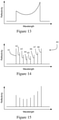
- the non-uniform gain profile of the gain section 24 of the laser may not be symmetric. It is possible to adjust the reflection spectrum of the chirped reflector to compensate for this by choosing the local reflection strength along the length of the grating to control the shape of the dishing of the reflection spectrum. It is therefore possible to produce a grating with an asymmetric reflection spectrum, as shown for example in Figure 13 .
- the phase change grating 28 acting as the rear reflector 27 may also be modified to compensate for the non-uniform gain profile of the gain section 24. This modification may be instead of or in addition to the dishing of the chirped grating 29 described above.
- the reflection spectrum of the comb grating should be modified by a dished envelope function. This can be seen in Figure 14 , which is a schematic graph showing the reflection profile 60 of a dished comb grating. The spectrum comprises a plurality of peaks 61-68 at discrete wavelengths, but the reflection of the outermost peaks 61, 68 is higher than the reflection of the inner peaks 64, 65, 66.
- phase changes to be other than ⁇ it is possible to further modify the shape of the dished comb reflection spectrum to provide asymmetry, as shown in Figure 15 . As mentioned above, this is useful where the gain profile is not symmetrical.
- the rear reflector may instead comprise, for example, a segmented grating or a sampled grating.
- a segmented grating may be dished in a similar manner to a chirped grating, by varying the reflective strength of individual segments. This may be done by varying the mark:space relative intensity or the mark:space width ratio, or by using the "deleted marks" approach also described above.
- the reflection spectrum of a chirped sampled grating may be dished by controlling the local reflection strengths at different wavelengths.
- Such asymmetric gratings may be used to compensate for asymmetric optical cavity losses.
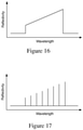
- a grating induces loss, so light reflected from a part of a grating far away from the gain section experiences more "round-trip" loss than light reflected from a part close to the gain section. It may therefore be beneficial to increase the reflective strength of the part of the grating far from the gain section to compensate.
- gratings with asymmetric profiles such as those of Figures 16 and 17
- dished gratings such as those shown in Figures 9 and 13-15 .
- a tunable laser has been described having a comb grating as a rear reflector and a chirped grating as a front reflector, but the invention may equally well be used with other designs of tunable laser.
- WO 03/012936 describes a laser having a phase change grating as a rear reflector and a segmented grating as a front reflector in addition to the phase change grating / chirped grating laser described above. In this case, the phase change grating or the segmented grating, or both, could be dished to compensate for the gain profile.
- Other tunable lasers have phase change gratings as front and rear reflectors and the reflection profiles of such gratings may be dished as described above.
Landscapes
- Physics & Mathematics (AREA)
- Electromagnetism (AREA)
- Optics & Photonics (AREA)
- General Physics & Mathematics (AREA)
- Condensed Matter Physics & Semiconductors (AREA)
- Engineering & Computer Science (AREA)
- Plasma & Fusion (AREA)
- Semiconductor Lasers (AREA)
- Diffracting Gratings Or Hologram Optical Elements (AREA)
Claims (7)
- Laser accordable (20) comprenant une section à gain (24) délimitée à chaque extrémité par un réflecteur (26, 27), au moins l'un des réflecteurs étant un réseau de Bragg adapté pour produire un spectre de réflexion comprenant un peigne (60) de pics de réflexion à des longueurs d'onde discrètes, les pics ayant des amplitudes de réflexion modulées par une fonction d'enveloppe non uniforme entre deux extrémités de longueur d'onde, le réseau comprenant une pluralité de sections de réseau périodiques séparées par des changements de phase (16), chacune des sections de grille ayant un pas constant,
caractérisé en ce que les longueurs des sections de réseau sont choisies pour que la fonction d'enveloppe comprenne des maxima aux deux extrémités de longueur d'onde, le spectre de réflexion ayant une fonction d'enveloppe d'amplitude conçue pour varier avec la longueur d'onde entre les deux extrémités de longueur d'onde de manière à compenser au moins partiellement les pertes de cavité optiques dépendant de la longueur d'onde dans le laser accordable. - Laser accordable selon la revendication 1, dans lequel la fonction d'enveloppe a une forme concave.
- Laser accordable selon la revendication 1 ou 2, dans lequel chaque changement de phase (16) entre les sections est de π radians.
- Laser accordable selon la revendication 1 ou 2, dans lequel la fonction d'enveloppe est asymétrique.
- Laser accordable selon la revendication 4, dans lequel les changements de phase (16) entre sections de réseau sont choisis pour contrôler l'asymétrie de la fonction enveloppe.
- Laser accordable selon l'une quelconque des revendications 1 à 5, dans lequel la section à gain (24) a un profil de gain de longueur d'onde non uniforme, et la fonction d'enveloppe d'amplitude est adaptée pour varier avec la longueur d'onde entre les deux extrémités de longueur d'onde d'une manière opposée au profil de gain de manière à compenser au moins partiellement le profil de gain non uniforme.
- Procédé de fourniture d'un laser accordable (20) selon l'une quelconque des revendications 1 à 6, dans lequel la section à gain (24) a un profil de gain de longueur d'onde non uniforme,
caractérisé en ce que les longueurs des sections de réseau sont choisies de telle sorte que le réseau de Bragg ait une fonction d'enveloppe qui soit non uniforme entre deux extrémités de longueur d'onde, de sorte que la fonction d'enveloppe inclue des maxima aux deux extrémités de longueur d'onde de manière à compenser au moins partiellement les pertes de cavité optiques dépendant de la longueur d'onde.
Applications Claiming Priority (3)
| Application Number | Priority Date | Filing Date | Title |
|---|---|---|---|
| GB0519799A GB2430760A (en) | 2005-09-29 | 2005-09-29 | Chirped Bragg grating structure |
| PCT/GB2006/050302 WO2007036749A2 (fr) | 2005-09-29 | 2006-09-22 | Structure de reseau de bragg |
| EP06779645.8A EP1929343B1 (fr) | 2005-09-29 | 2006-09-22 | Structure de reseau de bragg |
Related Parent Applications (1)
| Application Number | Title | Priority Date | Filing Date |
|---|---|---|---|
| EP06779645.8A Division EP1929343B1 (fr) | 2005-09-29 | 2006-09-22 | Structure de reseau de bragg |
Publications (2)
| Publication Number | Publication Date |
|---|---|
| EP2775329A1 EP2775329A1 (fr) | 2014-09-10 |
| EP2775329B1 true EP2775329B1 (fr) | 2022-03-16 |
Family
ID=35394934
Family Applications (2)
| Application Number | Title | Priority Date | Filing Date |
|---|---|---|---|
| EP06779645.8A Active EP1929343B1 (fr) | 2005-09-29 | 2006-09-22 | Structure de reseau de bragg |
| EP14166112.4A Active EP2775329B1 (fr) | 2005-09-29 | 2006-09-22 | Laser accordable avec structure de réseau de Bragg |
Family Applications Before (1)
| Application Number | Title | Priority Date | Filing Date |
|---|---|---|---|
| EP06779645.8A Active EP1929343B1 (fr) | 2005-09-29 | 2006-09-22 | Structure de reseau de bragg |
Country Status (5)
| Country | Link |
|---|---|
| US (2) | US7826508B2 (fr) |
| EP (2) | EP1929343B1 (fr) |
| JP (1) | JP4995824B2 (fr) |
| GB (1) | GB2430760A (fr) |
| WO (1) | WO2007036749A2 (fr) |
Families Citing this family (45)
| Publication number | Priority date | Publication date | Assignee | Title |
|---|---|---|---|---|
| GB2418995B (en) * | 2004-09-29 | 2006-08-16 | Bookham Technology Plc | Apodised binary grating |
| US8358888B2 (en) * | 2008-04-10 | 2013-01-22 | Ofs Fitel, Llc | Systems and techniques for generating Bessel beams |
| JP5434324B2 (ja) * | 2009-07-14 | 2014-03-05 | 富士通株式会社 | 反射型半導体光増幅器 |
| FR2959021B1 (fr) * | 2010-04-15 | 2012-07-27 | Commissariat Energie Atomique | Filtre optique mono ou multi-frequentiel et detecteur comportant un tel filtre |
| US8259304B2 (en) * | 2010-05-26 | 2012-09-04 | Gerard A Alphonse | Broadband discrete spectrum optical source |
| US8798414B2 (en) * | 2010-09-29 | 2014-08-05 | President And Fellows Of Harvard College | High quality factor photonic crystal nanobeam cavity and method of designing and making same |
| US20130321900A1 (en) * | 2010-12-01 | 2013-12-05 | Epicrystals Oy | Optical broadband filter and device comprising the same |
| JP2012226016A (ja) * | 2011-04-15 | 2012-11-15 | Toyota Industries Corp | センサ用光ファイバ |
| AU2011100725B4 (en) * | 2011-06-17 | 2011-09-22 | Innovia Security Pty Ltd | Diffraction grating |
| US8705584B2 (en) * | 2011-11-09 | 2014-04-22 | Corning Incorporated | DBR laser diode with symmetric aperiodically shifted grating phase |
| US9134807B2 (en) | 2012-03-02 | 2015-09-15 | Microsoft Technology Licensing, Llc | Pressure sensitive key normalization |
| US9075566B2 (en) | 2012-03-02 | 2015-07-07 | Microsoft Technoogy Licensing, LLC | Flexible hinge spine |
| US20130300590A1 (en) | 2012-05-14 | 2013-11-14 | Paul Henry Dietz | Audio Feedback |
| JP5692330B2 (ja) * | 2013-10-18 | 2015-04-01 | 住友電気工業株式会社 | 波長可変レーザ、波長可変レーザ装置、及び波長可変レーザ制御方法 |
| JP6275841B2 (ja) * | 2013-12-27 | 2018-02-07 | インテル・コーポレーション | 非対称光導波路格子共振器及びdbrレーザ |
| US9304235B2 (en) * | 2014-07-30 | 2016-04-05 | Microsoft Technology Licensing, Llc | Microfabrication |
| US10324733B2 (en) | 2014-07-30 | 2019-06-18 | Microsoft Technology Licensing, Llc | Shutdown notifications |
| US10254942B2 (en) | 2014-07-31 | 2019-04-09 | Microsoft Technology Licensing, Llc | Adaptive sizing and positioning of application windows |
| US9787576B2 (en) | 2014-07-31 | 2017-10-10 | Microsoft Technology Licensing, Llc | Propagating routing awareness for autonomous networks |
| US10678412B2 (en) | 2014-07-31 | 2020-06-09 | Microsoft Technology Licensing, Llc | Dynamic joint dividers for application windows |
| US10592080B2 (en) | 2014-07-31 | 2020-03-17 | Microsoft Technology Licensing, Llc | Assisted presentation of application windows |
| US9423360B1 (en) | 2015-02-09 | 2016-08-23 | Microsoft Technology Licensing, Llc | Optical components |
| US9535253B2 (en) | 2015-02-09 | 2017-01-03 | Microsoft Technology Licensing, Llc | Display system |
| US11086216B2 (en) | 2015-02-09 | 2021-08-10 | Microsoft Technology Licensing, Llc | Generating electronic components |
| US9827209B2 (en) | 2015-02-09 | 2017-11-28 | Microsoft Technology Licensing, Llc | Display system |
| US10317677B2 (en) | 2015-02-09 | 2019-06-11 | Microsoft Technology Licensing, Llc | Display system |
| US10018844B2 (en) | 2015-02-09 | 2018-07-10 | Microsoft Technology Licensing, Llc | Wearable image display system |
| US9372347B1 (en) | 2015-02-09 | 2016-06-21 | Microsoft Technology Licensing, Llc | Display system |
| US9513480B2 (en) | 2015-02-09 | 2016-12-06 | Microsoft Technology Licensing, Llc | Waveguide |
| US9429692B1 (en) | 2015-02-09 | 2016-08-30 | Microsoft Technology Licensing, Llc | Optical components |
| WO2016144831A1 (fr) | 2015-03-06 | 2016-09-15 | Apple Inc. | Commande indépendante de la longueur d'onde d'émission et de la puissance de sortie d'un laser à semi-conducteur |
| CN107624206B (zh) * | 2015-04-30 | 2022-05-27 | 苹果公司 | 包括集成调谐元件的游标效应dbr激光器 |
| CN105024279B (zh) * | 2015-06-16 | 2017-12-19 | 南京大学 | 一种阶梯相位布拉格光栅及其分布反馈半导体激光器的制备方法 |
| US11231544B2 (en) | 2015-11-06 | 2022-01-25 | Magic Leap, Inc. | Metasurfaces for redirecting light and methods for fabricating |
| JP6961619B2 (ja) | 2016-05-06 | 2021-11-05 | マジック リープ, インコーポレイテッドMagic Leap, Inc. | 光を再指向させるための非対称格子を有するメタ表面および製造方法 |
| IL307294A (en) | 2017-01-27 | 2023-11-01 | Magic Leap Inc | Diffraction gratings produced using a surface cell with differently oriented nanobeams |
| WO2018140502A1 (fr) | 2017-01-27 | 2018-08-02 | Magic Leap, Inc. | Revêtements antireflet pour méta-surfaces |
| CN108732667B (zh) * | 2017-04-17 | 2021-01-05 | 华为技术有限公司 | 一种超结构光栅和可调谐激光器 |
| CN113725725B (zh) | 2017-09-28 | 2025-05-02 | 苹果公司 | 使用量子阱混合技术的激光架构 |
| US11552454B1 (en) | 2017-09-28 | 2023-01-10 | Apple Inc. | Integrated laser source |
| FI128882B (en) * | 2017-12-22 | 2021-02-15 | Dispelix Oy | Optical waveguide and diffractive waveguide display |
| US11171464B1 (en) | 2018-12-14 | 2021-11-09 | Apple Inc. | Laser integration techniques |
| US12204155B2 (en) | 2021-09-24 | 2025-01-21 | Apple Inc. | Chip-to-chip optical coupling for photonic integrated circuits |
| US12426139B1 (en) | 2022-06-27 | 2025-09-23 | Apple Inc. | Feedback control of a diode element |
| CN116880010B (zh) * | 2023-09-06 | 2023-12-19 | 之江实验室 | 基于铌酸锂的集成环形布拉格金属光栅耦合器及制备方法 |
Family Cites Families (32)
| Publication number | Priority date | Publication date | Assignee | Title |
|---|---|---|---|---|
| US599546A (en) * | 1898-02-22 | Power-transmitter | ||
| US3141370A (en) | 1962-03-29 | 1964-07-21 | Ross Russel | Cymbal and sizzle combination |
| JPS622207A (ja) * | 1985-06-28 | 1987-01-08 | Hitachi Ltd | 回折格子およびその製法 |
| US4896325A (en) | 1988-08-23 | 1990-01-23 | The Regents Of The University Of California | Multi-section tunable laser with differing multi-element mirrors |
| US4993032A (en) * | 1989-12-28 | 1991-02-12 | General Dynamics Corp., Electronics Divn. | Monolithic temperature stabilized optical tuning circuit for channel separation in WDM systems utilizing tunable lasers |
| DE69128786T2 (de) * | 1990-06-06 | 1998-08-20 | Kol Ohr Corp., Wilmington, Del. | Abstimmbare Lichtquelle und faseroptische Systeme mit abstimmbarer Lichtquelle |
| US5091916A (en) * | 1990-09-28 | 1992-02-25 | At&T Bell Laboratories | Distributed reflector laser having improved side mode suppression |
| US5325392A (en) | 1992-03-06 | 1994-06-28 | Nippon Telegraph And Telephone Corporation | Distributed reflector and wavelength-tunable semiconductor laser |
| US5379318A (en) | 1994-01-31 | 1995-01-03 | Telefonaktiebolaget L M Ericsson | Alternating grating tunable DBR laser |
| US5633885A (en) * | 1994-09-29 | 1997-05-27 | Imra America, Inc. | Frequency chirp control and compensation for obtaining broad bandwidth ultrashort optical pulses from wavelength-tunable lasers |
| FR2737942B1 (fr) | 1995-08-18 | 1997-11-07 | Delorme Franck | Composant d'emission laser accordable en longueur d'onde par variation d'absorption |
| JP2004198435A (ja) * | 1995-11-01 | 2004-07-15 | Sumitomo Electric Ind Ltd | Otdr装置 |
| JP3534550B2 (ja) | 1995-11-01 | 2004-06-07 | 住友電気工業株式会社 | Otdr装置 |
| US5668900A (en) * | 1995-11-01 | 1997-09-16 | Northern Telecom Limited | Taper shapes for sidelobe suppression and bandwidth minimization in distributed feedback optical reflection filters |
| CA2228683C (fr) | 1998-02-20 | 2002-05-14 | Ivan Avrutsky | Lasers accordables par wdm a reseau superpose |
| US6088376A (en) * | 1998-03-16 | 2000-07-11 | California Institute Of Technology | Vertical-cavity-surface-emitting semiconductor devices with fiber-coupled optical cavity |
| GB9809583D0 (en) | 1998-05-06 | 1998-07-01 | Marconi Gec Ltd | Optical devices |
| US5999546A (en) * | 1998-09-22 | 1999-12-07 | Lucent Technologies Inc. | Magnetically tunable laser with wavelength latchability and optical communication system comprising such laser |
| US6204958B1 (en) * | 1998-10-08 | 2001-03-20 | Ciena Corporation | Optical amplifier having a substantially flat gain spectrum |
| US6993222B2 (en) * | 1999-03-03 | 2006-01-31 | Rj Mears, Llc | Optical filter device with aperiodically arranged grating elements |
| DE69928801T2 (de) | 1999-09-21 | 2006-08-03 | Bookham Technology Plc., Towcester | Stabilisierte Laserquelle |
| JP2001320127A (ja) * | 2000-05-02 | 2001-11-16 | Sumitomo Electric Ind Ltd | 半導体レーザ |
| GB0031646D0 (en) * | 2000-12-22 | 2001-02-07 | European Community | Method and apparatus for crack and fracture detection utilizing bragg gratings |
| FR2821495B1 (fr) | 2001-02-23 | 2004-08-27 | Cit Alcatel | Laser accordable de facon rapide et large |
| US6950576B1 (en) * | 2001-03-29 | 2005-09-27 | Sabeus Photonics, Inc. | Mode coupling devices with complex spectral profile |
| EP1413023B1 (fr) | 2001-07-30 | 2007-08-29 | Bookham Technology Plc. | Laser accordable |
| GB2378311A (en) * | 2001-08-03 | 2003-02-05 | Marconi Caswell Ltd | Tunable Laser |
| EP1291985A1 (fr) * | 2001-09-07 | 2003-03-12 | Corning O.T.I. S.p.A. | Filtre optique d'aplatissement du gain , amplificateur optique muni d'un tel filtre et méthode de fabrication |
| JP2003298184A (ja) * | 2002-03-29 | 2003-10-17 | Anritsu Corp | 半導体レーザモジュール及び該半導体レーザモジュールを用いた波長合成器 |
| US7046704B2 (en) * | 2002-07-01 | 2006-05-16 | Mrv Communication Ltd. | Tunable laser with a fixed and stable wavelength grid especially useful for WDM in fiber optic communication systems |
| US7139128B2 (en) * | 2003-01-06 | 2006-11-21 | Polychromix Corporation | Diffraction grating having high throughput efficiency |
| GB2418995B (en) | 2004-09-29 | 2006-08-16 | Bookham Technology Plc | Apodised binary grating |
-
2005
- 2005-09-29 GB GB0519799A patent/GB2430760A/en not_active Withdrawn
-
2006
- 2006-09-22 EP EP06779645.8A patent/EP1929343B1/fr active Active
- 2006-09-22 EP EP14166112.4A patent/EP2775329B1/fr active Active
- 2006-09-22 JP JP2008532883A patent/JP4995824B2/ja active Active
- 2006-09-22 WO PCT/GB2006/050302 patent/WO2007036749A2/fr not_active Ceased
- 2006-09-22 US US12/088,136 patent/US7826508B2/en active Active
-
2010
- 2010-09-24 US US12/889,517 patent/US8457172B2/en active Active
Also Published As
| Publication number | Publication date |
|---|---|
| EP1929343A2 (fr) | 2008-06-11 |
| EP1929343B1 (fr) | 2014-04-30 |
| GB2430760A (en) | 2007-04-04 |
| US7826508B2 (en) | 2010-11-02 |
| JP4995824B2 (ja) | 2012-08-08 |
| JP2009510506A (ja) | 2009-03-12 |
| WO2007036749A3 (fr) | 2007-06-07 |
| EP2775329A1 (fr) | 2014-09-10 |
| US20110069727A1 (en) | 2011-03-24 |
| GB0519799D0 (en) | 2005-11-09 |
| WO2007036749A2 (fr) | 2007-04-05 |
| US20080232411A1 (en) | 2008-09-25 |
| US8457172B2 (en) | 2013-06-04 |
Similar Documents
| Publication | Publication Date | Title |
|---|---|---|
| EP2775329B1 (fr) | Laser accordable avec structure de réseau de Bragg | |
| JP4458413B2 (ja) | チューナブルレーザ | |
| JP3962014B2 (ja) | 抽出格子ブラッグ反射器に結合された抽出格子分布帰還波長可変半導体レーザ | |
| US6141370A (en) | Superimposed grating WDM tunable lasers | |
| JP5552793B2 (ja) | 半導体回折格子素子、及び、半導体レーザ | |
| US7106778B2 (en) | Tuneable laser | |
| EP1413021B1 (fr) | Laser accordable | |
| US7830927B2 (en) | Bragg grating reflection strength control | |
| US12174370B2 (en) | Synthesized aperiodic gratings and method of manufacture | |
| US7680374B2 (en) | Apodised binary Bragg grating | |
| US8160410B2 (en) | Bragg reflector grating | |
| JP2008294371A (ja) | 半導体発光素子 | |
| JPH06175169A (ja) | 光周波数変換素子 | |
| JPH0661571A (ja) | 分布光反射器及びそれを用いた半導体レーザ |
Legal Events
| Date | Code | Title | Description |
|---|---|---|---|
| PUAI | Public reference made under article 153(3) epc to a published international application that has entered the european phase |
Free format text: ORIGINAL CODE: 0009012 |
|
| 17P | Request for examination filed |
Effective date: 20140425 |
|
| AC | Divisional application: reference to earlier application |
Ref document number: 1929343 Country of ref document: EP Kind code of ref document: P |
|
| AK | Designated contracting states |
Kind code of ref document: A1 Designated state(s): AT BE BG CH CY CZ DE DK EE ES FI FR GB GR HU IE IS IT LI LT LU LV MC NL PL PT RO SE SI SK TR |
|
| R17P | Request for examination filed (corrected) |
Effective date: 20140905 |
|
| RBV | Designated contracting states (corrected) |
Designated state(s): AT BE BG CH CY CZ DE DK EE ES FI FR GB GR HU IE IS IT LI LT LU LV MC NL PL PT RO SE SI SK TR |
|
| RAP1 | Party data changed (applicant data changed or rights of an application transferred) |
Owner name: OCLARO TECHNOLOGY LIMITED |
|
| STAA | Information on the status of an ep patent application or granted ep patent |
Free format text: STATUS: EXAMINATION IS IN PROGRESS |
|
| 17Q | First examination report despatched |
Effective date: 20171010 |
|
| RAP1 | Party data changed (applicant data changed or rights of an application transferred) |
Owner name: LUMENTUM TECHNOLOGY UK LIMITED |
|
| GRAP | Despatch of communication of intention to grant a patent |
Free format text: ORIGINAL CODE: EPIDOSNIGR1 |
|
| STAA | Information on the status of an ep patent application or granted ep patent |
Free format text: STATUS: GRANT OF PATENT IS INTENDED |
|
| INTG | Intention to grant announced |
Effective date: 20210927 |
|
| GRAS | Grant fee paid |
Free format text: ORIGINAL CODE: EPIDOSNIGR3 |
|
| GRAA | (expected) grant |
Free format text: ORIGINAL CODE: 0009210 |
|
| STAA | Information on the status of an ep patent application or granted ep patent |
Free format text: STATUS: THE PATENT HAS BEEN GRANTED |
|
| AC | Divisional application: reference to earlier application |
Ref document number: 1929343 Country of ref document: EP Kind code of ref document: P |
|
| AK | Designated contracting states |
Kind code of ref document: B1 Designated state(s): AT BE BG CH CY CZ DE DK EE ES FI FR GB GR HU IE IS IT LI LT LU LV MC NL PL PT RO SE SI SK TR |
|
| REG | Reference to a national code |
Ref country code: GB Ref legal event code: FG4D |
|
| REG | Reference to a national code |
Ref country code: CH Ref legal event code: EP |
|
| REG | Reference to a national code |
Ref country code: DE Ref legal event code: R096 Ref document number: 602006060297 Country of ref document: DE |
|
| REG | Reference to a national code |
Ref country code: IE Ref legal event code: FG4D |
|
| REG | Reference to a national code |
Ref country code: AT Ref legal event code: REF Ref document number: 1476300 Country of ref document: AT Kind code of ref document: T Effective date: 20220415 |
|
| REG | Reference to a national code |
Ref country code: LT Ref legal event code: MG9D |
|
| REG | Reference to a national code |
Ref country code: NL Ref legal event code: MP Effective date: 20220316 |
|
| PG25 | Lapsed in a contracting state [announced via postgrant information from national office to epo] |
Ref country code: SE Free format text: LAPSE BECAUSE OF FAILURE TO SUBMIT A TRANSLATION OF THE DESCRIPTION OR TO PAY THE FEE WITHIN THE PRESCRIBED TIME-LIMIT Effective date: 20220316 Ref country code: LT Free format text: LAPSE BECAUSE OF FAILURE TO SUBMIT A TRANSLATION OF THE DESCRIPTION OR TO PAY THE FEE WITHIN THE PRESCRIBED TIME-LIMIT Effective date: 20220316 Ref country code: BG Free format text: LAPSE BECAUSE OF FAILURE TO SUBMIT A TRANSLATION OF THE DESCRIPTION OR TO PAY THE FEE WITHIN THE PRESCRIBED TIME-LIMIT Effective date: 20220616 |
|
| REG | Reference to a national code |
Ref country code: AT Ref legal event code: MK05 Ref document number: 1476300 Country of ref document: AT Kind code of ref document: T Effective date: 20220316 |
|
| PG25 | Lapsed in a contracting state [announced via postgrant information from national office to epo] |
Ref country code: LV Free format text: LAPSE BECAUSE OF FAILURE TO SUBMIT A TRANSLATION OF THE DESCRIPTION OR TO PAY THE FEE WITHIN THE PRESCRIBED TIME-LIMIT Effective date: 20220316 Ref country code: GR Free format text: LAPSE BECAUSE OF FAILURE TO SUBMIT A TRANSLATION OF THE DESCRIPTION OR TO PAY THE FEE WITHIN THE PRESCRIBED TIME-LIMIT Effective date: 20220617 Ref country code: FI Free format text: LAPSE BECAUSE OF FAILURE TO SUBMIT A TRANSLATION OF THE DESCRIPTION OR TO PAY THE FEE WITHIN THE PRESCRIBED TIME-LIMIT Effective date: 20220316 |
|
| PG25 | Lapsed in a contracting state [announced via postgrant information from national office to epo] |
Ref country code: NL Free format text: LAPSE BECAUSE OF FAILURE TO SUBMIT A TRANSLATION OF THE DESCRIPTION OR TO PAY THE FEE WITHIN THE PRESCRIBED TIME-LIMIT Effective date: 20220316 |
|
| PG25 | Lapsed in a contracting state [announced via postgrant information from national office to epo] |
Ref country code: SK Free format text: LAPSE BECAUSE OF FAILURE TO SUBMIT A TRANSLATION OF THE DESCRIPTION OR TO PAY THE FEE WITHIN THE PRESCRIBED TIME-LIMIT Effective date: 20220316 Ref country code: RO Free format text: LAPSE BECAUSE OF FAILURE TO SUBMIT A TRANSLATION OF THE DESCRIPTION OR TO PAY THE FEE WITHIN THE PRESCRIBED TIME-LIMIT Effective date: 20220316 Ref country code: PT Free format text: LAPSE BECAUSE OF FAILURE TO SUBMIT A TRANSLATION OF THE DESCRIPTION OR TO PAY THE FEE WITHIN THE PRESCRIBED TIME-LIMIT Effective date: 20220718 Ref country code: ES Free format text: LAPSE BECAUSE OF FAILURE TO SUBMIT A TRANSLATION OF THE DESCRIPTION OR TO PAY THE FEE WITHIN THE PRESCRIBED TIME-LIMIT Effective date: 20220316 Ref country code: EE Free format text: LAPSE BECAUSE OF FAILURE TO SUBMIT A TRANSLATION OF THE DESCRIPTION OR TO PAY THE FEE WITHIN THE PRESCRIBED TIME-LIMIT Effective date: 20220316 Ref country code: CZ Free format text: LAPSE BECAUSE OF FAILURE TO SUBMIT A TRANSLATION OF THE DESCRIPTION OR TO PAY THE FEE WITHIN THE PRESCRIBED TIME-LIMIT Effective date: 20220316 Ref country code: AT Free format text: LAPSE BECAUSE OF FAILURE TO SUBMIT A TRANSLATION OF THE DESCRIPTION OR TO PAY THE FEE WITHIN THE PRESCRIBED TIME-LIMIT Effective date: 20220316 |
|
| PG25 | Lapsed in a contracting state [announced via postgrant information from national office to epo] |
Ref country code: PL Free format text: LAPSE BECAUSE OF FAILURE TO SUBMIT A TRANSLATION OF THE DESCRIPTION OR TO PAY THE FEE WITHIN THE PRESCRIBED TIME-LIMIT Effective date: 20220316 Ref country code: IS Free format text: LAPSE BECAUSE OF FAILURE TO SUBMIT A TRANSLATION OF THE DESCRIPTION OR TO PAY THE FEE WITHIN THE PRESCRIBED TIME-LIMIT Effective date: 20220716 |
|
| REG | Reference to a national code |
Ref country code: DE Ref legal event code: R097 Ref document number: 602006060297 Country of ref document: DE |
|
| PLBE | No opposition filed within time limit |
Free format text: ORIGINAL CODE: 0009261 |
|
| STAA | Information on the status of an ep patent application or granted ep patent |
Free format text: STATUS: NO OPPOSITION FILED WITHIN TIME LIMIT |
|
| PG25 | Lapsed in a contracting state [announced via postgrant information from national office to epo] |
Ref country code: DK Free format text: LAPSE BECAUSE OF FAILURE TO SUBMIT A TRANSLATION OF THE DESCRIPTION OR TO PAY THE FEE WITHIN THE PRESCRIBED TIME-LIMIT Effective date: 20220316 |
|
| 26N | No opposition filed |
Effective date: 20221219 |
|
| PG25 | Lapsed in a contracting state [announced via postgrant information from national office to epo] |
Ref country code: SI Free format text: LAPSE BECAUSE OF FAILURE TO SUBMIT A TRANSLATION OF THE DESCRIPTION OR TO PAY THE FEE WITHIN THE PRESCRIBED TIME-LIMIT Effective date: 20220316 |
|
| PG25 | Lapsed in a contracting state [announced via postgrant information from national office to epo] |
Ref country code: MC Free format text: LAPSE BECAUSE OF FAILURE TO SUBMIT A TRANSLATION OF THE DESCRIPTION OR TO PAY THE FEE WITHIN THE PRESCRIBED TIME-LIMIT Effective date: 20220316 |
|
| REG | Reference to a national code |
Ref country code: CH Ref legal event code: PL |
|
| GBPC | Gb: european patent ceased through non-payment of renewal fee |
Effective date: 20220922 |
|
| REG | Reference to a national code |
Ref country code: BE Ref legal event code: MM Effective date: 20220930 |
|
| PG25 | Lapsed in a contracting state [announced via postgrant information from national office to epo] |
Ref country code: LU Free format text: LAPSE BECAUSE OF NON-PAYMENT OF DUE FEES Effective date: 20220922 |
|
| PG25 | Lapsed in a contracting state [announced via postgrant information from national office to epo] |
Ref country code: LI Free format text: LAPSE BECAUSE OF NON-PAYMENT OF DUE FEES Effective date: 20220930 Ref country code: IT Free format text: LAPSE BECAUSE OF FAILURE TO SUBMIT A TRANSLATION OF THE DESCRIPTION OR TO PAY THE FEE WITHIN THE PRESCRIBED TIME-LIMIT Effective date: 20220316 Ref country code: IE Free format text: LAPSE BECAUSE OF NON-PAYMENT OF DUE FEES Effective date: 20220922 Ref country code: FR Free format text: LAPSE BECAUSE OF NON-PAYMENT OF DUE FEES Effective date: 20220930 Ref country code: CH Free format text: LAPSE BECAUSE OF NON-PAYMENT OF DUE FEES Effective date: 20220930 |
|
| PG25 | Lapsed in a contracting state [announced via postgrant information from national office to epo] |
Ref country code: BE Free format text: LAPSE BECAUSE OF NON-PAYMENT OF DUE FEES Effective date: 20220930 |
|
| PG25 | Lapsed in a contracting state [announced via postgrant information from national office to epo] |
Ref country code: GB Free format text: LAPSE BECAUSE OF NON-PAYMENT OF DUE FEES Effective date: 20220922 |
|
| PG25 | Lapsed in a contracting state [announced via postgrant information from national office to epo] |
Ref country code: HU Free format text: LAPSE BECAUSE OF FAILURE TO SUBMIT A TRANSLATION OF THE DESCRIPTION OR TO PAY THE FEE WITHIN THE PRESCRIBED TIME-LIMIT; INVALID AB INITIO Effective date: 20060922 |
|
| PG25 | Lapsed in a contracting state [announced via postgrant information from national office to epo] |
Ref country code: CY Free format text: LAPSE BECAUSE OF FAILURE TO SUBMIT A TRANSLATION OF THE DESCRIPTION OR TO PAY THE FEE WITHIN THE PRESCRIBED TIME-LIMIT Effective date: 20220316 |
|
| PGFP | Annual fee paid to national office [announced via postgrant information from national office to epo] |
Ref country code: DE Payment date: 20240926 Year of fee payment: 19 |
|
| PG25 | Lapsed in a contracting state [announced via postgrant information from national office to epo] |
Ref country code: TR Free format text: LAPSE BECAUSE OF FAILURE TO SUBMIT A TRANSLATION OF THE DESCRIPTION OR TO PAY THE FEE WITHIN THE PRESCRIBED TIME-LIMIT Effective date: 20220316 |