EP2775512B1 - Halbleiterbauelemente - Google Patents
Halbleiterbauelemente Download PDFInfo
- Publication number
- EP2775512B1 EP2775512B1 EP14157382.4A EP14157382A EP2775512B1 EP 2775512 B1 EP2775512 B1 EP 2775512B1 EP 14157382 A EP14157382 A EP 14157382A EP 2775512 B1 EP2775512 B1 EP 2775512B1
- Authority
- EP
- European Patent Office
- Prior art keywords
- semiconductor chip
- chip
- interface
- semiconductor
- redistribution layer
- Prior art date
- Legal status (The legal status is an assumption and is not a legal conclusion. Google has not performed a legal analysis and makes no representation as to the accuracy of the status listed.)
- Active
Links
Images




Classifications
-
- H—ELECTRICITY
- H10—SEMICONDUCTOR DEVICES; ELECTRIC SOLID-STATE DEVICES NOT OTHERWISE PROVIDED FOR
- H10W—GENERIC PACKAGES, INTERCONNECTIONS, CONNECTORS OR OTHER CONSTRUCTIONAL DETAILS OF DEVICES COVERED BY CLASS H10
- H10W70/00—Package substrates; Interposers; Redistribution layers [RDL]
- H10W70/60—Insulating or insulated package substrates; Interposers; Redistribution layers
- H10W70/611—Insulating or insulated package substrates; Interposers; Redistribution layers for connecting multiple chips together
-
- H—ELECTRICITY
- H10—SEMICONDUCTOR DEVICES; ELECTRIC SOLID-STATE DEVICES NOT OTHERWISE PROVIDED FOR
- H10W—GENERIC PACKAGES, INTERCONNECTIONS, CONNECTORS OR OTHER CONSTRUCTIONAL DETAILS OF DEVICES COVERED BY CLASS H10
- H10W70/00—Package substrates; Interposers; Redistribution layers [RDL]
- H10W70/01—Manufacture or treatment
- H10W70/05—Manufacture or treatment of insulating or insulated package substrates, or of interposers, or of redistribution layers
- H10W70/08—Manufacture or treatment of insulating or insulated package substrates, or of interposers, or of redistribution layers by depositing layers on the chip or wafer, e.g. "chip-first" RDLs
- H10W70/09—Manufacture or treatment of insulating or insulated package substrates, or of interposers, or of redistribution layers by depositing layers on the chip or wafer, e.g. "chip-first" RDLs extending onto an encapsulation that laterally surrounds the chip or wafer, e.g. fan-out wafer level package [FOWLP] RDLs
-
- H—ELECTRICITY
- H10—SEMICONDUCTOR DEVICES; ELECTRIC SOLID-STATE DEVICES NOT OTHERWISE PROVIDED FOR
- H10W—GENERIC PACKAGES, INTERCONNECTIONS, CONNECTORS OR OTHER CONSTRUCTIONAL DETAILS OF DEVICES COVERED BY CLASS H10
- H10W70/00—Package substrates; Interposers; Redistribution layers [RDL]
- H10W70/60—Insulating or insulated package substrates; Interposers; Redistribution layers
- H10W70/611—Insulating or insulated package substrates; Interposers; Redistribution layers for connecting multiple chips together
- H10W70/614—Insulating or insulated package substrates; Interposers; Redistribution layers for connecting multiple chips together the multiple chips being integrally enclosed
-
- H—ELECTRICITY
- H10—SEMICONDUCTOR DEVICES; ELECTRIC SOLID-STATE DEVICES NOT OTHERWISE PROVIDED FOR
- H10W—GENERIC PACKAGES, INTERCONNECTIONS, CONNECTORS OR OTHER CONSTRUCTIONAL DETAILS OF DEVICES COVERED BY CLASS H10
- H10W70/00—Package substrates; Interposers; Redistribution layers [RDL]
- H10W70/60—Insulating or insulated package substrates; Interposers; Redistribution layers
- H10W70/62—Insulating or insulated package substrates; Interposers; Redistribution layers characterised by their interconnections
- H10W70/63—Vias, e.g. via plugs
- H10W70/635—Through-vias
-
- H—ELECTRICITY
- H10—SEMICONDUCTOR DEVICES; ELECTRIC SOLID-STATE DEVICES NOT OTHERWISE PROVIDED FOR
- H10W—GENERIC PACKAGES, INTERCONNECTIONS, CONNECTORS OR OTHER CONSTRUCTIONAL DETAILS OF DEVICES COVERED BY CLASS H10
- H10W90/00—Package configurations
-
- H—ELECTRICITY
- H10—SEMICONDUCTOR DEVICES; ELECTRIC SOLID-STATE DEVICES NOT OTHERWISE PROVIDED FOR
- H10W—GENERIC PACKAGES, INTERCONNECTIONS, CONNECTORS OR OTHER CONSTRUCTIONAL DETAILS OF DEVICES COVERED BY CLASS H10
- H10W70/00—Package substrates; Interposers; Redistribution layers [RDL]
- H10W70/60—Insulating or insulated package substrates; Interposers; Redistribution layers
-
- H—ELECTRICITY
- H10—SEMICONDUCTOR DEVICES; ELECTRIC SOLID-STATE DEVICES NOT OTHERWISE PROVIDED FOR
- H10W—GENERIC PACKAGES, INTERCONNECTIONS, CONNECTORS OR OTHER CONSTRUCTIONAL DETAILS OF DEVICES COVERED BY CLASS H10
- H10W70/00—Package substrates; Interposers; Redistribution layers [RDL]
- H10W70/60—Insulating or insulated package substrates; Interposers; Redistribution layers
- H10W70/62—Insulating or insulated package substrates; Interposers; Redistribution layers characterised by their interconnections
- H10W70/65—Shapes or dispositions of interconnections
- H10W70/654—Top-view layouts
-
- H—ELECTRICITY
- H10—SEMICONDUCTOR DEVICES; ELECTRIC SOLID-STATE DEVICES NOT OTHERWISE PROVIDED FOR
- H10W—GENERIC PACKAGES, INTERCONNECTIONS, CONNECTORS OR OTHER CONSTRUCTIONAL DETAILS OF DEVICES COVERED BY CLASS H10
- H10W70/00—Package substrates; Interposers; Redistribution layers [RDL]
- H10W70/60—Insulating or insulated package substrates; Interposers; Redistribution layers
- H10W70/62—Insulating or insulated package substrates; Interposers; Redistribution layers characterised by their interconnections
- H10W70/66—Conductive materials thereof
-
- H—ELECTRICITY
- H10—SEMICONDUCTOR DEVICES; ELECTRIC SOLID-STATE DEVICES NOT OTHERWISE PROVIDED FOR
- H10W—GENERIC PACKAGES, INTERCONNECTIONS, CONNECTORS OR OTHER CONSTRUCTIONAL DETAILS OF DEVICES COVERED BY CLASS H10
- H10W72/00—Interconnections or connectors in packages
- H10W72/01—Manufacture or treatment
-
- H—ELECTRICITY
- H10—SEMICONDUCTOR DEVICES; ELECTRIC SOLID-STATE DEVICES NOT OTHERWISE PROVIDED FOR
- H10W—GENERIC PACKAGES, INTERCONNECTIONS, CONNECTORS OR OTHER CONSTRUCTIONAL DETAILS OF DEVICES COVERED BY CLASS H10
- H10W72/00—Interconnections or connectors in packages
- H10W72/071—Connecting or disconnecting
- H10W72/072—Connecting or disconnecting of bump connectors
- H10W72/07251—Connecting or disconnecting of bump connectors characterised by changes in properties of the bump connectors during connecting
- H10W72/07252—Connecting or disconnecting of bump connectors characterised by changes in properties of the bump connectors during connecting changes in structures or sizes
-
- H—ELECTRICITY
- H10—SEMICONDUCTOR DEVICES; ELECTRIC SOLID-STATE DEVICES NOT OTHERWISE PROVIDED FOR
- H10W—GENERIC PACKAGES, INTERCONNECTIONS, CONNECTORS OR OTHER CONSTRUCTIONAL DETAILS OF DEVICES COVERED BY CLASS H10
- H10W72/00—Interconnections or connectors in packages
- H10W72/071—Connecting or disconnecting
- H10W72/072—Connecting or disconnecting of bump connectors
- H10W72/07251—Connecting or disconnecting of bump connectors characterised by changes in properties of the bump connectors during connecting
- H10W72/07254—Connecting or disconnecting of bump connectors characterised by changes in properties of the bump connectors during connecting changes in dispositions
-
- H—ELECTRICITY
- H10—SEMICONDUCTOR DEVICES; ELECTRIC SOLID-STATE DEVICES NOT OTHERWISE PROVIDED FOR
- H10W—GENERIC PACKAGES, INTERCONNECTIONS, CONNECTORS OR OTHER CONSTRUCTIONAL DETAILS OF DEVICES COVERED BY CLASS H10
- H10W72/00—Interconnections or connectors in packages
- H10W72/20—Bump connectors, e.g. solder bumps or copper pillars; Dummy bumps; Thermal bumps
- H10W72/221—Structures or relative sizes
- H10W72/227—Multiple bumps having different sizes
-
- H—ELECTRICITY
- H10—SEMICONDUCTOR DEVICES; ELECTRIC SOLID-STATE DEVICES NOT OTHERWISE PROVIDED FOR
- H10W—GENERIC PACKAGES, INTERCONNECTIONS, CONNECTORS OR OTHER CONSTRUCTIONAL DETAILS OF DEVICES COVERED BY CLASS H10
- H10W72/00—Interconnections or connectors in packages
- H10W72/20—Bump connectors, e.g. solder bumps or copper pillars; Dummy bumps; Thermal bumps
- H10W72/241—Dispositions, e.g. layouts
-
- H—ELECTRICITY
- H10—SEMICONDUCTOR DEVICES; ELECTRIC SOLID-STATE DEVICES NOT OTHERWISE PROVIDED FOR
- H10W—GENERIC PACKAGES, INTERCONNECTIONS, CONNECTORS OR OTHER CONSTRUCTIONAL DETAILS OF DEVICES COVERED BY CLASS H10
- H10W72/00—Interconnections or connectors in packages
- H10W72/20—Bump connectors, e.g. solder bumps or copper pillars; Dummy bumps; Thermal bumps
- H10W72/241—Dispositions, e.g. layouts
- H10W72/244—Dispositions, e.g. layouts relative to underlying supporting features, e.g. bond pads, RDLs or vias
-
- H—ELECTRICITY
- H10—SEMICONDUCTOR DEVICES; ELECTRIC SOLID-STATE DEVICES NOT OTHERWISE PROVIDED FOR
- H10W—GENERIC PACKAGES, INTERCONNECTIONS, CONNECTORS OR OTHER CONSTRUCTIONAL DETAILS OF DEVICES COVERED BY CLASS H10
- H10W72/00—Interconnections or connectors in packages
- H10W72/20—Bump connectors, e.g. solder bumps or copper pillars; Dummy bumps; Thermal bumps
- H10W72/241—Dispositions, e.g. layouts
- H10W72/247—Dispositions of multiple bumps
-
- H—ELECTRICITY
- H10—SEMICONDUCTOR DEVICES; ELECTRIC SOLID-STATE DEVICES NOT OTHERWISE PROVIDED FOR
- H10W—GENERIC PACKAGES, INTERCONNECTIONS, CONNECTORS OR OTHER CONSTRUCTIONAL DETAILS OF DEVICES COVERED BY CLASS H10
- H10W72/00—Interconnections or connectors in packages
- H10W72/20—Bump connectors, e.g. solder bumps or copper pillars; Dummy bumps; Thermal bumps
- H10W72/251—Materials
- H10W72/252—Materials comprising solid metals or solid metalloids, e.g. PbSn, Ag or Cu
-
- H—ELECTRICITY
- H10—SEMICONDUCTOR DEVICES; ELECTRIC SOLID-STATE DEVICES NOT OTHERWISE PROVIDED FOR
- H10W—GENERIC PACKAGES, INTERCONNECTIONS, CONNECTORS OR OTHER CONSTRUCTIONAL DETAILS OF DEVICES COVERED BY CLASS H10
- H10W72/00—Interconnections or connectors in packages
- H10W72/20—Bump connectors, e.g. solder bumps or copper pillars; Dummy bumps; Thermal bumps
- H10W72/29—Bond pads specially adapted therefor
-
- H—ELECTRICITY
- H10—SEMICONDUCTOR DEVICES; ELECTRIC SOLID-STATE DEVICES NOT OTHERWISE PROVIDED FOR
- H10W—GENERIC PACKAGES, INTERCONNECTIONS, CONNECTORS OR OTHER CONSTRUCTIONAL DETAILS OF DEVICES COVERED BY CLASS H10
- H10W72/00—Interconnections or connectors in packages
- H10W72/823—Interconnections through encapsulations, e.g. pillars through molded resin on a lateral side a chip
-
- H—ELECTRICITY
- H10—SEMICONDUCTOR DEVICES; ELECTRIC SOLID-STATE DEVICES NOT OTHERWISE PROVIDED FOR
- H10W—GENERIC PACKAGES, INTERCONNECTIONS, CONNECTORS OR OTHER CONSTRUCTIONAL DETAILS OF DEVICES COVERED BY CLASS H10
- H10W72/00—Interconnections or connectors in packages
- H10W72/851—Dispositions of multiple connectors or interconnections
- H10W72/874—On different surfaces
-
- H—ELECTRICITY
- H10—SEMICONDUCTOR DEVICES; ELECTRIC SOLID-STATE DEVICES NOT OTHERWISE PROVIDED FOR
- H10W—GENERIC PACKAGES, INTERCONNECTIONS, CONNECTORS OR OTHER CONSTRUCTIONAL DETAILS OF DEVICES COVERED BY CLASS H10
- H10W72/00—Interconnections or connectors in packages
- H10W72/90—Bond pads, in general
- H10W72/921—Structures or relative sizes of bond pads
- H10W72/922—Bond pads being integral with underlying chip-level interconnections
-
- H—ELECTRICITY
- H10—SEMICONDUCTOR DEVICES; ELECTRIC SOLID-STATE DEVICES NOT OTHERWISE PROVIDED FOR
- H10W—GENERIC PACKAGES, INTERCONNECTIONS, CONNECTORS OR OTHER CONSTRUCTIONAL DETAILS OF DEVICES COVERED BY CLASS H10
- H10W72/00—Interconnections or connectors in packages
- H10W72/90—Bond pads, in general
- H10W72/941—Dispositions of bond pads
- H10W72/9413—Dispositions of bond pads on encapsulations
-
- H—ELECTRICITY
- H10—SEMICONDUCTOR DEVICES; ELECTRIC SOLID-STATE DEVICES NOT OTHERWISE PROVIDED FOR
- H10W—GENERIC PACKAGES, INTERCONNECTIONS, CONNECTORS OR OTHER CONSTRUCTIONAL DETAILS OF DEVICES COVERED BY CLASS H10
- H10W72/00—Interconnections or connectors in packages
- H10W72/90—Bond pads, in general
- H10W72/941—Dispositions of bond pads
- H10W72/942—Dispositions of bond pads relative to underlying supporting features, e.g. bond pads, RDLs or vias
-
- H—ELECTRICITY
- H10—SEMICONDUCTOR DEVICES; ELECTRIC SOLID-STATE DEVICES NOT OTHERWISE PROVIDED FOR
- H10W—GENERIC PACKAGES, INTERCONNECTIONS, CONNECTORS OR OTHER CONSTRUCTIONAL DETAILS OF DEVICES COVERED BY CLASS H10
- H10W72/00—Interconnections or connectors in packages
- H10W72/90—Bond pads, in general
- H10W72/951—Materials of bond pads
- H10W72/952—Materials of bond pads comprising metals or metalloids, e.g. PbSn, Ag or Cu
-
- H—ELECTRICITY
- H10—SEMICONDUCTOR DEVICES; ELECTRIC SOLID-STATE DEVICES NOT OTHERWISE PROVIDED FOR
- H10W—GENERIC PACKAGES, INTERCONNECTIONS, CONNECTORS OR OTHER CONSTRUCTIONAL DETAILS OF DEVICES COVERED BY CLASS H10
- H10W74/00—Encapsulations, e.g. protective coatings
-
- H—ELECTRICITY
- H10—SEMICONDUCTOR DEVICES; ELECTRIC SOLID-STATE DEVICES NOT OTHERWISE PROVIDED FOR
- H10W—GENERIC PACKAGES, INTERCONNECTIONS, CONNECTORS OR OTHER CONSTRUCTIONAL DETAILS OF DEVICES COVERED BY CLASS H10
- H10W74/00—Encapsulations, e.g. protective coatings
- H10W74/10—Encapsulations, e.g. protective coatings characterised by their shape or disposition
- H10W74/15—Encapsulations, e.g. protective coatings characterised by their shape or disposition on active surfaces of flip-chip devices, e.g. underfills
-
- H—ELECTRICITY
- H10—SEMICONDUCTOR DEVICES; ELECTRIC SOLID-STATE DEVICES NOT OTHERWISE PROVIDED FOR
- H10W—GENERIC PACKAGES, INTERCONNECTIONS, CONNECTORS OR OTHER CONSTRUCTIONAL DETAILS OF DEVICES COVERED BY CLASS H10
- H10W90/00—Package configurations
- H10W90/20—Configurations of stacked chips
- H10W90/297—Configurations of stacked chips characterised by the through-semiconductor vias [TSVs] in the stacked chips
-
- H—ELECTRICITY
- H10—SEMICONDUCTOR DEVICES; ELECTRIC SOLID-STATE DEVICES NOT OTHERWISE PROVIDED FOR
- H10W—GENERIC PACKAGES, INTERCONNECTIONS, CONNECTORS OR OTHER CONSTRUCTIONAL DETAILS OF DEVICES COVERED BY CLASS H10
- H10W90/00—Package configurations
- H10W90/701—Package configurations characterised by the relative positions of pads or connectors relative to package parts
-
- H—ELECTRICITY
- H10—SEMICONDUCTOR DEVICES; ELECTRIC SOLID-STATE DEVICES NOT OTHERWISE PROVIDED FOR
- H10W—GENERIC PACKAGES, INTERCONNECTIONS, CONNECTORS OR OTHER CONSTRUCTIONAL DETAILS OF DEVICES COVERED BY CLASS H10
- H10W90/00—Package configurations
- H10W90/701—Package configurations characterised by the relative positions of pads or connectors relative to package parts
- H10W90/721—Package configurations characterised by the relative positions of pads or connectors relative to package parts of bump connectors
- H10W90/722—Package configurations characterised by the relative positions of pads or connectors relative to package parts of bump connectors between stacked chips
-
- H—ELECTRICITY
- H10—SEMICONDUCTOR DEVICES; ELECTRIC SOLID-STATE DEVICES NOT OTHERWISE PROVIDED FOR
- H10W—GENERIC PACKAGES, INTERCONNECTIONS, CONNECTORS OR OTHER CONSTRUCTIONAL DETAILS OF DEVICES COVERED BY CLASS H10
- H10W90/00—Package configurations
- H10W90/701—Package configurations characterised by the relative positions of pads or connectors relative to package parts
- H10W90/721—Package configurations characterised by the relative positions of pads or connectors relative to package parts of bump connectors
- H10W90/724—Package configurations characterised by the relative positions of pads or connectors relative to package parts of bump connectors between a chip and a stacked insulating package substrate, interposer or RDL
-
- H—ELECTRICITY
- H10—SEMICONDUCTOR DEVICES; ELECTRIC SOLID-STATE DEVICES NOT OTHERWISE PROVIDED FOR
- H10W—GENERIC PACKAGES, INTERCONNECTIONS, CONNECTORS OR OTHER CONSTRUCTIONAL DETAILS OF DEVICES COVERED BY CLASS H10
- H10W90/00—Package configurations
- H10W90/701—Package configurations characterised by the relative positions of pads or connectors relative to package parts
- H10W90/731—Package configurations characterised by the relative positions of pads or connectors relative to package parts of die-attach connectors
- H10W90/734—Package configurations characterised by the relative positions of pads or connectors relative to package parts of die-attach connectors between a chip and a stacked insulating package substrate, interposer or RDL
Definitions
- the present disclosure relates generally to semiconductor devices.
- 3D chip stacks two or more semiconductor chips may be stacked on top of each other. Adjacent chips in the stack may be electrically coupled to one another via an interface.
- the physical design of the interface may be predetermined or fixed according to a given standard. For example, geometric dimensions of the interface, such as length, width, pad pitch, etc., may be prescribed by the standard. For example with increasing scaling in semiconductor technology, chip sizes may come close to or become even smaller than the prescribed geometric dimensions of the interface. For example, a chip may have a length that is smaller than a length of the interface as prescribed by the standard. In this case, it may be desirable to modify the chip to fit to the partly larger interface.
- US 2012/0077313 A1 describes a semiconductor device having a plurality of mold-sealed semiconductor chips connected to a flip chip-mounted semiconductor chip by rewiring and an insulating layer.
- KR 2011 0048733 A describes a stack chip package using RDL and TSV to make a device thin by forming a plurality of memory chips which are laminated in the upper corner of a lower chip and reducing the thickness of the device.
- a semiconductor device is provided as set out in claim 1.
- a feature e.g. a layer “over” a side or surface
- the feature e.g. the layer
- the word “over”, used herein to describe forming a feature, e.g. a layer “over” a side or surface, may be used to mean that the feature, e.g. the layer, may be disposed or formed "indirectly on” the implied side or surface with one or more additional layers being arranged between the implied side or surface and the formed layer.
- Coupled and/or “electrically coupled” and/or “connected” and/or “electrically connected”, used herein to describe a feature being connected to at least one other implied feature, are not meant to mean that the feature and the at least one other implied feature must be directly coupled or connected together; intervening features may be provided between the feature and at least one other implied feature.
- a plurality of may be understood to include any integer number greater than or equal to two, i.e. "two”, “three”, “four”, “five”, etc.
- standardized as used herein may, for example, be understood as meaning “according to a standard” or “defined by a standard”, for example according to or defined by a standard developed by a standardization committee, body or organization such as JEDEC (Joint Electron Device Engineering Council) or others.
- the present disclosure relates to three-dimensional (3D) chip stacks such as, for example, stacks of logic and memory chips.
- 3D chip stacks such as, for example, stacks of logic and memory chips.
- the following description will mainly refer to logic/memory chip stacks as an example, however the present disclosure is not limited to this case and may be applied to stacking of any two or more chips in general.
- the stacking of logic chips on logic chips the stacking of logic chips with RF chips, analog/mixed signal chips or power chips
- the stacking of chips with sensors with micro electro mechanical systems (MEMS) or CMOS image sensors, and any other combination of 3D stacks.
- MEMS micro electro mechanical systems
- Memory chips or a stack of memory chips may, for example, include or consist of dynamic random access memory (DRAM) memory chips with a 'Wide I/O (Input/Output)' interface (JEDEC standard).
- DRAM dynamic random access memory
- JEDEC 'Wide I/O (Input/Output)' interface
- 3D logic/memory chip stacks with 'wide I/O' interface is the fact that the size of the logic/memory interface is fixed to 0.52 mm ⁇ 5.25 mm according to the JEDEC standard.
- a 3D logic memory stack for e.g. mobile applications may include a logic chip 101 (e.g. CPU, etc.) with TSVs (through-silicon vias) 102 connected by a 'wide I/O interface' 103 to a single memory chip or a stack of memory chips 104.
- this 3D logic/memory chip stack may be connected to a (multi-layer) ball grid array (BGA) laminate package by flip-chip connections, as shown in Fig. 1 .
- the size of the logic chip 101 is larger than the extension of the 'wide I/O' interface 103 (e.g. here with ⁇ -bumps and TSVs).
- Fig. 2 shows in a plan view 200 the standardized JEDEC 'wide I/O' logic-memory interface (LMI) 103 on a typical 'wide I/O' DRAM memory 204.
- the 'wide I/O' interface 103 may include a high density contact grid 205 including a plurality of electrically conductive contacts.
- the 'wide I/O' interface according to the JEDEC standard may have a length of 5.25 mm and a width of 0.52 mm.
- a conventional approach to address the aforementioned issue may be to increase the chip size (here length of chip) until it is long/large enough to fit to the 'wide I/O' interface standard, as is shown in Fig. 3 .
- Fig. 3 shows in a plan view 300 that the chip size of a small logic chip may be extended (on silicon) until it fits to the size of the 'wide I/O' interface 103, wherein reference sign 301 denotes the logic chip having the original chip size and reference sign 301' denotes the logic chip with extended chip size.
- the logic chip 301 having the original chip size has a length 106 that is shorter than a length 107 of the interface 103
- the logic chip 301' with extended chip size has a length 108 that is longer than the length 107 of the interface 103.
- the conventional approach to extend the chip size may be extremely expensive, because it requires an additional 'dummy' chip area (that is, chip area which is not needed for active or passive circuitry) which may need to be manufactured in an expensive silicon wafer technology (e.g. beyond 28 nm node).
- the present disclosure provides a relatively cheap (cost effective) way to increase the size (area) of the logic chip, or in general, of any first chip that shall be coupled to a second chip via an interface that is partly larger than the chip size of the first chip.
- semiconductor devices in accordance with one or more aspects described herein may apply a relatively cheap (cost effective) fan-out WLP (wafer level package) or eWLB (embedded wafer level package ball grid array) approach to gain enough space for the interface or for the placement of one or more electrically conductive contacts (e.g. pads) connecting to the interface (e.g. logic-memory interface, e.g. 'wide I/O' interface).
- WLP wafer level package
- eWLB embedded wafer level package ball grid array
- An extension layer including or composed of a relatively cheap chip encapsulation material e.g. a plastic material such as a molding material, or the like
- a redistribution layer (RDL) disposed over the extension layer is used to reroute one or more interface connections disposed outside (e.g. at least partially outside, e.g. fully outside) a boundary of the chip (in other words, outside the original chip area) to one or more electrically conductive contacts of the chip inside the boundary of the chip (inside the original chip area).
- the RDL may be a single level RDL or a multi-level RDL (i.e. an RDL having two or more levels or layers).
- a multi-level RDL may, for example, be used in cases where a relatively large number of interface interconnections lie outside the boundary of the chip (outside the original chip area).
- the present disclosure proposes for chips (e.g. logic chips) that are smaller than the extension of a standardized chip-to-chip interface (e.g. standardized logic-memory interface, e.g. 'wide I/O' memory interface according to JEDEC standard) to make use of a fan-out WLP (eWLB) chip extension with a single-level or multi-level RDL to provide the connection to the larger interface (e.g. memory interface).
- a standardized chip-to-chip interface e.g. standardized logic-memory interface, e.g. 'wide I/O' memory interface according to JEDEC standard
- eWLB fan-out WLP
- This approach may be significantly more cost effective (cheaper) than the conventional approach to increase the area of the chip, e.g. increase the silicon area of a highly advanced logic chip.
- the eWLB RDL is able to reroute one or more interface connections (e.g. 'wide I/O' connections) to appropriate areas of the small chip, where the placement of a through-via (e.g. through-silicon via (TSV)) or an array of through-vias (e.g. TSVs) is possible.
- a through-via e.g. through-silicon via (TSV)
- TSVs through-silicon vias
- the fan-out eWLB RDL may be disposed over one side (e.g. back side) of the chip only or, alternatively, may be disposed over both sides of the chip (i.e. over the back side and over the front side of the chip (e.g. logic chip)).
- TSV through-via
- the through-via connections on the chip e.g. logic chip
- all or a part of the connections may be provided by through-vias (e.g. through mold vias (TMVs)) extending through the extension layer (e.g. mold compound) in the fan-out area of the eWLB package.
- TMVs through mold vias
- These through-vias (e.g. TMVs) in combination with the RDL levels are able to connect the interface contacts (e.g. 'wide I/O' pads) with the front side (active circuit area) of the small chip (e.g. logic chip) and to an interposer (e.g. laminate interposer) (if necessary even bypassing the small chip (e.g. logic chip)).
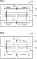
- Fig. 4 is a plan view 400 of an example of a semiconductor device in accordance with one or more aspects described herein.
- the semiconductor device includes a first semiconductor chip 401.
- the first semiconductor chip 401 may be a (small) logic chip, similar to logic chip 301 in Fig. 3 .
- the first semiconductor chip 401 may be another type of chip different from a logic chip, and may be any type of chip in general.
- the first semiconductor chip 401 is to be electrically coupled to a second semiconductor chip 404 via a standardized chip-to-chip interface 403.
- the second semiconductor chip 404 may be a memory chip (e.g. a DRAM chip).
- the chip-to-chip interface 403 may be a logic-memory interface, e.g. a 'wide I/O' logic-memory interface, similar to interface 103 shown in Fig. 3 .
- the second semiconductor chip 404 may be another type of chip different from a memory chip, and may be any type of chip in general, and the interface 403 may be another type of interface, e.g.
- logic-memory interface or a type of interface different from a logic-memory interface, and may, for example, be any type of interface having a predefined or fixed size (prescribed by some standard), which is at least partly larger than the size (area) of the first semiconductor chip 401.
- the first semiconductor chip 401 has a length 406 that is smaller than a length 407 of the standardized chip-to-chip interface 403.
- the length 406 of the first semiconductor chip 401 may be smaller than 5.25 mm.
- the length 406 may be smaller than some value different from 5.25 mm, as will be readily understood.
- a part of the chip-to-chip interface 403 extends laterally beyond a boundary 401a of the first semiconductor chip 401.
- the interface 403 does not fully fit onto the area of the first semiconductor chip 401 of the semiconductor device.
- the interface 403 is longer than the chip 401.
- the semiconductor device further includes an extension layer 405 extending laterally from the boundary 401a of the first semiconductor chip 401.
- the extension layer 405 may extend from all lateral sides of the first semiconductor chip 401 (in the example shown, from all four lateral sides of the chip 401). That is, the extension layer 405 may laterally enclose the first semiconductor chip 401.
- the extension layer 405 extends only from some of the lateral sides, e.g. from one, two, or three of the four lateral sides of the first semiconductor chip 401, for example from two opposite lateral sides as shown in a plan view 500 in Fig. 5 illustrating another example of a semiconductor device, or from one lateral side as shown in a plan view 600 in Fig. 6 illustrating another example of a semiconductor device.
- the extension layer 405 may be formed such that the combined area of the first semiconductor chip 401 and the extension layer 405 may be large enough to fit the size or area of the standardized chip-to-chip interface 403, for example the size or area of a 'wide I/O' logic-memory interface.
- the extension layer 405 is formed such that a combined length 408 of the first semiconductor chip 401 and the extension layer 405 is larger than the length of the interface 403.
- the extension layer 405 may include or may be composed of a material (or materials) different from the first semiconductor chip 401, for example an insulating material, for example a chip encapsulant material, e.g. a plastic material, e.g. a molding material (mold compound).
- a molding material e.g. a molding material (mold compound).
- the molding material (mold compound) may be a composite material consisting of a resin (e.g. epoxy resin) and a filler material (e.g. fused silica).
- the extension layer 405 may serve as a fan-out extension (fan-out region) of the first semiconductor chip 401 to accommodate one or more electrically conductive contacts (e.g. pads) to be coupled to one or more electrically conductive contacts (e.g. pads) of the interface 403 that lie outside the chip 401's boundary 401a.
- electrically conductive contacts of the interface 403 that would no longer fit onto the semiconductor chip 401 because of the first semiconductor chip 401's small size may now be coupled to electrically conductive contacts disposed over the extension layer 405, and a redistribution layer (not shown in Figs. 4 to 6 , see e.g. Figs. 7 to 10 ) used to provide electrical coupling of those contacts with the first semiconductor chip 401.
- a fan-out WLP (eWLB) package may be provided, which may have a single level or, if needed, a multi-level redistribution layer (RDL) with electrically conductive contacts (e.g. contact pads) in the top RDL metallization level.
- RDL redistribution layer
- the non-fitting electrically conductive contacts may be shifted or rearranged elsewhere and may be connected by the single- or multi-level RDL wiring, as described herein below with reference to Figs. 7 to 10 .
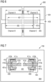
- Fig. 7 is a plan view 700 of an example of a semiconductor device, including a redistribution layer 409 configured to reroute interface connections, e.g. electrically conductive contacts, 410 of the standardized chip-to-chip interface 403, disposed outside the boundary 401a of the first semiconductor chip 401 to electrically conductive contacts (e.g. pads) 411a (of the first semiconductor chip 401) inside the boundary 401a of the first semiconductor chip 401.
- interface connections e.g. electrically conductive contacts, 410 of the standardized chip-to-chip interface 403, disposed outside the boundary 401a of the first semiconductor chip 401 to electrically conductive contacts (e.g. pads) 411a (of the first semiconductor chip 401) inside the boundary 401a of the first semiconductor chip 401.
- logic-memory interface connections e.g. 'wide I/O' interface connections
- memory chip 404 or memory chip stack
- the redistribution layer 409 is disposed over at least one side of the extension layer 405 and the first semiconductor chip 401.
- the redistribution layer 409 may include or may be composed of an electrically conductive material, for example, a metal or metal alloy such as copper, aluminum, or an alloy containing copper and/or aluminum.
- the redistribution layer 409 may include one or more electrically conductive contacts (e.g.
- pads to be coupled to respective electrical contacts of the chip-to-chip interface 403, and may include one or more conductive traces connecting the electrically conductive contacts (e.g. pads) of the redistribution layer 409 to the electrically conductive contacts (e.g. pads) of the first semiconductor chip 401.
- One or more electrically conductive contacts 410a of the interface 403 lying completely outside the boundary 401a of the first semiconductor chip 401 may be rerouted to one or more electrically conductive contacts 411a lying inside the boundary 401a by means of the redistribution layer 409.
- electrically conductive contacts 410b of the interface 403 may also be possible to reroute one or more electrically conductive contacts 410b of the interface 403 that lie inside the chip boundary 401a but close to the chip boundary 401a (for example, contacts 410b having a lateral distance of less than or equal to about 100 ⁇ m, e.g. less than or equal to about 50 ⁇ m, from the chip boundary 401a) to one or more electrically conductive contacts 411a of the first semiconductor chip 401 that are disposed well inside the chip boundary 401a (e.g. contacts 411a having a lateral distance of greater than about 50 ⁇ m, e.g. greater than about 100 ⁇ m, from the chip boundary 401a), as shown.
- electrically conductive contacts e.g.
- pads) 410c of the interface 403 that lie well within the boundary 401a of the first semiconductor chip 401 may or may not be rerouted and may be coupled to corresponding electrically conductive contacts (e.g. pads) 411b (not shown in Fig. 7 , see e.g. Fig. 8 ) of the first semiconductor chip 401.
- Fig. 8 is a cross-sectional view 800 of a semiconductor device, which may be configured as a three-dimensional (3D) logic-memory stack.
- the semiconductor device includes the first semiconductor chip 401, which may be configured as a logic chip (e.g. central processing unit (CPU), graphics processing unit (GPU), application processor (AP), base band modem, micro controller, or the like), and the second semiconductor chip 404, which may be configured as a memory chip, e.g. as a DRAM chip, and coupled to the first semiconductor chip 401 via the standardized chip-to-chip interface 403, which may be a logic-memory interface (e.g. a 'wide I/O logic-memory interface).
- the second semiconductor chip 404 may be part of a chip stack 804, e.g. a memory chip stack, e.g. a 'wide I/O' memory stack, e.g.
- a DRAM stack including at least one additional semiconductor chip (e.g. memory chip, e.g. DRAM chip) stacked on top of the second semiconductor chip 404.
- additional semiconductor chip e.g. memory chip, e.g. DRAM chip
- three additional semiconductor chips 404', 404", and 404′′′ are stacked on top of the second semiconductor chip 404, resulting in a total of four chips, however the number of chips in the stack 804 may be different from four, e.g. two, three, five, six, seven, etc.
- only the second semiconductor chip 404 may be disposed over the first semiconductor chip 401.
- the logic-memory interface (e.g. 'wide I/O' interface) 403 may extend over the original logic chip size. In other words, the interface 403 extends beyond the (lateral) boundary 401a of the first semiconductor chip 401, as shown.
- An extension layer 405 e.g. fan-out eWLB extension
- a part of the extension layer 405 may be disposed between the first semiconductor chip 401 and the second semiconductor chip 404, for example over a first side 401b of the logic chip 401 facing the second semiconductor chip 404.
- the first side 401b may be a back side of the first semiconductor chip 401.
- the first semiconductor chip 401 may be arranged as in a typical flip chip arrangement with a second side 401c (front side or active side) of the first semiconductor chip 401 facing down (facing away from the interface 403 in this case), e.g. towards a ball grid array as shown in Fig. 8 .
- a single-level redistribution layer (RDL) 409 may be disposed over the extension layer 405 for rerouting interface connections (e.g. 'wide I/O' connections), e.g. electrically conductive contacts (e.g. pads), 410 (see Fig. 7 ) of the interface 403 lying outside the boundary 401a of the logic chip 401 to chip areas out of the drawing plane of Fig. 8 , e.g. to rearranged or shifted electrically conductive contacts 411 of the first semiconductor chip 401 (see Fig. 7 ).
- a multi-level RDL may be used.
- the redistribution layer 409 or one or more electrically conductive contacts (e.g. pads) 409a of the redistribution layer 409, may be coupled to corresponding electrically conductive contacts (e.g. pads) 411a, 411b of the first semiconductor chip 401 by means of one or more through-vias 412 (e.g. through-encapsulant vias, e.g. through-mold vias (TMVs)) in the extension layer 405.
- the electrically conductive contact(s) 411a, 411b of the first semiconductor chip 401 coupled to the redistribution layer 409 (or to the electrically conductive contact(s) 409a of the redistribution layer 409) may be disposed over the first side 401b (e.g.
- the first semiconductor chip 401 may include one or more through-vias 417 (e.g. through-silicon vias (TSVs)) coupled to the electrically conductive contact(s) 411a, 411b disposed over the first side 401b and extending to the second side 401c (e.g. front side) of the first semiconductor chip 401 opposite the first side 401b.
- TSVs through-silicon vias
- the chips of the chip stack 804 may also include one more through-vias 418 (e.g. through-silicon vias (TSVs)) extending in each case from a front side to a back side of the respective chip 404, 404', 404'' to allow for electrical coupling between the individual chips of the chip stack 804 and thus to the first semiconductor chip 401 via the interface 403.
- TSVs through-silicon vias
- the through-vias 417 through the first semiconductor chip 401 and the through-vias 418 through the chip stack 804 may be located underneath (or above) the respective electrically conductive contacts (e.g. pads) of the interface 403 (e.g. the 'wide I/O' logic/memory interface with 40 ⁇ m ⁇ 50 ⁇ m pad pitch), as shown in Fig. 8 .
- the through-vias 417 may be located elsewhere and the connection between the electrically conductive contacts (e.g. pads) of the interface 403 (e.g. 'wide I/O' interface pads) and the respective through-vias 417 may be provided by a rerouting in the single- or multi-level RDL 409 of the fan-out eWLB package and/or by a back side metallization of the first semiconductor chip 401.
- a rerouting in the single- or multi-level RDL 409 of the fan-out eWLB package and/or by a back side metallization of the first semiconductor chip 401.
- the first semiconductor chip 401 may be coupled to a (e.g. multi-level) ball grid array (BGA) package, including for example, an interposer 413 (e.g. a laminate interposer having one or more metallization or interconnect levels) connected to one or more electrically conductive contacts (e.g. pads) on the second side (e.g. front side) 401c of the first semiconductor chip 401 by means of one or more electrical connectors 414 (e.g. solder bumps (as shown), or metal (e.g. Cu) pillars), and a printed circuit board (PCB) 415 connected to the interposer 413 by means of one or more electrical connectors 416 (e.g. solder bumps, as shown).
- BGA ball grid array
- the semiconductor chip 401 may also be arranged such that its front side (or active side) faces away from the BGA and towards the second semiconductor chip 404 or chip stack 804.
- a double-sided eWLB extension with single or multi-level RDL on both sides may be used.
- an eWLB RDL may be used on the back side of the first semiconductor chip (e.g. logic chip) connecting to the standardized interface 403, e.g. logic-memory interface, e.g. 'wide I/O memory interface' (as shown in Fig. 8 ), and additionally on the chip front side to connect to an interposer 413, e.g. BGA laminate, as shown in Figs. 9 and 10 .
- Fig. 9 and Fig. 10 respectively, show a cross-sectional view 900 and a plan view 1000 of a semiconductor device including a redistribution layer 409 for rerouting interface connections (e.g. electrically conductive contacts, e.g. pads) of the standardized chip-to-chip interface 403, wherein a first portion 409' of the redistribution layer 409 is disposed over the first side (e.g. back side) 401b and a second portion 409'' of the redistribution layer 409 is disposed over the second side (e.g. front side) 401c of the first semiconductor chip 401.
- the extension layer 405 e.g.
- eWLB chip extension may laterally extend from the boundary 401a of the first semiconductor chip 401, e.g. from all lateral sides of the first semiconductor chip 401, as shown in Fig. 10 , alternatively from only some (e.g. one, two, or three) lateral sides of the first semiconductor chip 401.
- a part of the extension layer 405 may be disposed over the first side 401b of the first semiconductor chip 401 (facing the chip-to-chip interface 403), and a further part of the extension layer 405 may be disposed over the second side 401c of the first semiconductor chip 401.
- the extension layer 405 may thus at least partially, e.g. fully, enclose the first semiconductor chip 401.
- the semiconductor device may be configured as a three-dimensional (3D) logic-memory stack, wherein the first semiconductor chip 401 may be a logic chip and may be coupled (via the chip-to-chip interface 403, e.g. logic-memory interface, e.g. 'wide I/O' interface) to a memory chip stack 804 (e.g. DRAM stack) including the second semiconductor chip 404 and one or more additional semiconductor chips 404', 404", 404′′′ which may be configured as memory chips (e.g. DRAM chips).
- a memory chip stack 804 e.g. DRAM stack
- additional semiconductor chips 404', 404", 404′′′ which may be configured as memory chips (e.g. DRAM chips).
- Reference signs that are the same as in Fig. 8 may denote the same elements as there and will not described in detail again here for sake of brevity. Reference is made to the description above.
- One or more electrically conductive contacts (e.g. pads) 410 of the standardized interface 403 may be rerouted via the redistribution layer 409.
- the contacts 410 may include one or more contacts 410a lying at least partially outside, e.g. fully outside, the boundary 401a of the first semiconductor chip 401, and may possibly also include one or more contacts 410b that lie inside the chip boundary 401a but close to the chip boundary 401a, as described above.
- One or more through-vias 412c may be provided in the extension layer 405 to electrically couple the rerouted contacts 410 (e.g. contacts 410a and/or 410b) to one or more electrically conductive contacts (e.g. pads) of the first semiconductor chip 401 disposed over the second side (e.g. front side) 401c.
- TMVs through-mold vias
- the respective through-via(s) 412c may be coupled to the first portion 409' of the redistribution layer 409 disposed over the first side 401b of the first semiconductor chip 401 and to the second portion 409'' of the redistribution layer 409 disposed over the second side 401c of the first semiconductor chip 401, and the second portion 409'' of the redistribution layer 409 may further be coupled to the one or more electrically conductive contacts (e.g. pads) of the first semiconductor chip 401 disposed over the second side 401c of the first semiconductor chip 401, for example by means of one or more through-vias 412b (e.g. through-encapsulant vias, e.g.
- through-vias 412b e.g. through-encapsulant vias, e.g.
- TMVs through-mold vias
- the second portion 409'' of the redistribution layer 409 may further be coupled to the interposer 413, e.g. via one or more electrical connectors 414 such as solder bumps (as shown) or metal pillars (e.g. Cu pillars), to provide electrical coupling of the semiconductor device to external devices.
- one or more of the through-vias 412c leading through the extension layer 405 are coupled to a part of the second portion 409'' of the redistribution layer 409 that may be coupled to the interposer 413 but not to the first semiconductor chip 401.
- a part of the second portion 409'' of the redistribution layer 409 may be coupled to the interposer 413 but not to the first semiconductor chip 401.
- the through-via 412c on the right-hand side of the figure is coupled to a part of the second portion 409'' of the redistribution layer 409 that is coupled to the interposer 413 but not to the first semiconductor chip 401, whereas the through-via 412c on the left-hand side of the figure is coupled to a part of the second portion 409'' of the redistribution layer 409 that is coupled (by means of a through via 412) to the first semiconductor chip 401.
- One or more electrically conductive contacts (e.g. pads) 410c of the interface 403 that lie well inside the chip boundary 401a may be coupled to one or more electrically conductive contacts 411b of the first semiconductor chip 401 that are disposed over the first side (e.g. back side) 401b of the first semiconductor chip 401, e.g. by means of one or more through-vias (e.g. TMVs) 412a disposed in the part of the extension layer 405 that is disposed over the first side (e.g. back side) 401b of the first semiconductor chip 401.
- TMVs through-vias
- Figs. 9 and 10 show an example of a semiconductor device wherein a standardized chip-to-chip interface 403 (e.g. logic-memory interface, e.g. 'wide I/O' interface) extends over the original chip size of a first semiconductor chip (e.g. logic chip) 401, an extension layer 405 (e.g. fan-out eWLB extension) of the first semiconductor chip (e.g. (small) logic chip) 401 having a single-level RDL 409 on both sides (i.e. on a chip back side 401b connecting to the interface (e.g. 'wide I/O' interface) 403 and on a chip front side (e.g.
- a standardized chip-to-chip interface 403 e.g. logic-memory interface, e.g. 'wide I/O' interface
- an extension layer 405 e.g. fan-out eWLB extension
- an interposer e.g. laminate interposer 413 and to the first semiconductor chip (e.g. logic chip) 401
- through-vias e.g. through-mold vias (TMVs)
- TMVs through-mold vias
- 412c couple electrically conductive contacts of the interface 403 (e.g. 'wide I/O' interface pads) via the redistribution layer 409 (e.g. eWLB RDL) (on back side 401b and front side 401c) with the active side (e.g. on-chip interconnect BEOL) of the chip (see left through-via 412c in Fig. 9 ) or directly with the interposer (e.g. laminate interposer) 413 bypassing the first semiconductor chip (e.g. logic chip) 401 (see right through-via 412c in Fig. 9 ).
- TMVs through-mold vias
- the examples described herein above in connection with the figures mainly discuss the case that only one lateral dimension (e.g. the length) of the first semiconductor chip is smaller than the respective dimension of the standardized chip-to-chip interface.
- more than one lateral dimension of the first semiconductor chip e.g. length and width
- the extension layer e.g. eWLB fan-out region
- the extension layer may be configured to increase the original chip area such that the interface fits onto the chip having the extension.
- the extension layer and redistribution layer may, for example, be formed using known manufacturing processes for manufacturing eWLB packages.
Landscapes
- Semiconductor Memories (AREA)
- Internal Circuitry In Semiconductor Integrated Circuit Devices (AREA)
- Semiconductor Integrated Circuits (AREA)
Claims (14)
- Halbleitervorrichtung, die Folgendes umfasst:einen ersten Halbleiterchip (401);einen zweiten Halbleiterchip (404), wobei der erste Halbleiterchip (401) mindestens einen Kontakt aufweist, um elektrisch mit dem zweiten Halbleiterchip (404) gekoppelt zu werden, der eine Schnittstelle (403) mit standardisierten geometrischen Abmessungen aufweist, und wobei der zweite Halbleiterchip (404) über die Schnittstelle (403) elektrisch mit dem ersten Halbleiterchip (401) gekoppelt ist;eine Erweiterungsschicht (405), die sich lateral von einer Grenze (401a) des ersten Halbleiterchips (401) erstreckt, wobei eine kombinierte laterale Abmessung des ersten Halbleiterchips (401) und der Erweiterungsschicht (405) entlang der mindestens einen Richtung größer oder gleich der lateralen Abmessung der Schnittstelle (403) entlang der mindestens einen Richtung ist; undeine Umverteilungsschicht (409), die über mindestens einer Seite der Erweiterungsschicht (405) und des ersten Halbleiterchips (401) angeordnet ist, wobei die Umverteilungsschicht (409) dazu ausgelegt ist, mindestens einen Kontakt des ersten Halbleiterchips (401) elektrisch mit mindestens einem Kontakt der Schnittstelle (403) zu koppeln, dadurch gekennzeichnet, dass:sich mindestens ein Teil der Schnittstelle (403) lateral über die Grenze (401a) des ersten Halbleiterchips (401) hinaus erstreckt; undeine laterale Abmessung (406) des ersten Halbleiterchips (401) entlang mindestens einer Richtung kleiner als eine laterale Abmessung (407) der Schnittstelle (403) entlang der mindestens einen Richtung ist.
- Halbleitervorrichtung nach Anspruch 1, wobei der mindestens eine Kontakt der Schnittstelle (403) mindestens teilweise außerhalb der Grenze (401a) des ersten Halbleiterchips (401) angeordnet ist.
- Halbleitervorrichtung nach Anspruch 1, wobei die standardisierte Schnittstelle (403) eine standardisierte Chip-zu-Chip-Schnittstelle (403) ist.
- Halbleitervorrichtung nach Anspruch 2, wobei die Umverteilungsschicht (409) mindestens einen Kontakt umfasst, der zur Kopplung mit dem mindestens einen Kontakt der Schnittstelle (403) ausgelegt ist, der mindestens teilweise außerhalb der Grenze (401a) des ersten Halbleiterchips (401) angeordnet ist.
- Halbleitervorrichtung nach Anspruch 4, wobei die Umverteilungsschicht (409) ferner mindestens einen Kontakt umfasst, der zur Kopplung mit mindestens einem Kontakt der Schnittstelle (403) ausgelegt ist, der innerhalb der Grenze (401a) des ersten Halbleiterchips (401) angeordnet ist.
- Halbleitervorrichtung nach Anspruch 1, wobei die Umverteilungsschicht (409) über einer Rückseite (401b) des ersten Halbleiterchips (401) angeordnet ist.
- Halbleitervorrichtung nach Anspruch 5, wobei die Erweiterungsschicht (405) über der Rückseite (401b) des ersten Halbleiterchips (401) zwischen dem ersten Halbleiterchip (401) und der Umverteilungsschicht (409) angeordnet ist.
- Halbleitervorrichtung nach Anspruch 7, wobei die Erweiterungsschicht (405) zusätzlich mindestens eine Durchkontaktierung umfasst, die mindestens einen Kontakt des ersten Halbleiterchips (401) elektrisch mit der Umverteilungsschicht (409) koppelt.
- Halbleitervorrichtung nach Anspruch 1, wobei die Umverteilungsschicht (409) einen ersten Teil, der über einer ersten Seite des ersten Halbleiterchips (401) angeordnet ist, und einen zweiten Teil, der über einer zweiten Seite des ersten Halbleiterchips (401) gegenüber der ersten Seite angeordnet ist, umfasst; oderwobei die Erweiterungsschicht (405) aus einem Material besteht, das sich von dem ersten Halbleiterchip (401) unterscheidet; oderwobei die Erweiterungsschicht (405) den ersten Halbleiterchip (401) zumindest teilweise einkapselt.
- Halbleitervorrichtung nach Anspruch 9,wobei der erste Teil der Umverteilungsschicht (409) mindestens einen Kontakt umfasst, der zur Kopplung mit dem mindestens einen Kontakt der Schnittstelle (403) ausgelegt ist, der mindestens teilweise außerhalb der Grenze (401a) des ersten Halbleiterchips (401) angeordnet ist,wobei die Erweiterungsschicht (405) mindestens eine Durchkontaktierung umfasst, die den ersten Teil der Umverteilungsschicht (409) elektrisch mit dem zweiten Teil der Umverteilungsschicht (409) koppelt.
- Halbleitervorrichtung nach Anspruch 10,
wobei der erste Halbleiterchip (401) mindestens einen Kontakt umfasst, der über der zweiten Seite des ersten Halbleiterchips (401) angeordnet und elektrisch mit dem zweiten Teil der Umverteilungsschicht (409) gekoppelt ist, wobei vorzugsweise die erste Seite eine Rückseite (401b) des ersten Halbleiterchips (401) ist und die zweite Seite eine Vorderseite (401c) des ersten Halbleiterchips (401) ist. - Halbleitervorrichtung nach Anspruch 1,wobei der erste Halbleiterchip (401) ein Logikchip ist und der zweite Halbleiterchip (404) ein Speicherchip ist; oderferner umfassend mindestens einen zusätzlichen Halbleiterchip, der über einer von dem ersten Halbleiterchip (401) abgewandten Seite des zweiten Halbleiterchips (404) angeordnet und elektrisch mit dem zweiten Halbleiterchip (404) gekoppelt ist.
- Halbleitervorrichtung nach Anspruch 1:wobei der erste Halbleiterchip (401) eine erste Vielzahl von Kontakten aufweist;wobei die Umverteilungsschicht (409) eine zweite Vielzahl von Kontakten aufweist, die elektrisch mit der ersten Vielzahl von Kontakten gekoppelt ist,wobei mindestens ein Kontakt der zweiten Vielzahl von Kontakten mindestens teilweise außerhalb der lateralen Grenze des ersten Halbleiterchips (401) angeordnet ist,wobei die zweite Vielzahl von Kontakten gemäß einem vorbestimmten Schnittstellenstandard angeordnet ist.
- Halbleitervorrichtung nach Anspruch 13, die ferner Folgendes umfasst:der zweite Halbleiterchip (404) weist eine dritte Vielzahl von Kontakten auf, die gemäß dem vorbestimmten Schnittstellenstandard angeordnet sind,wobei die dritte Vielzahl von Kontakten mit der zweiten Vielzahl von Kontakten in Kontakt steht, vorzugsweisewobei der erste Halbleiterchip (401) ein Logikchip ist und der zweite Halbleiterchip (404) ein Speicherchip ist undwobei der vorbestimmte Schnittstellenstandard ein Logik-Speicher-Schnittstellenstandard ist, und wobei vorzugsweise außerdem die Erweiterungsschicht (405) mindestens eine Durchkontaktierung umfasst, die mindestens einen Kontakt der ersten Vielzahl von Kontakten elektrisch mit mindestens einem Kontakt der zweiten Vielzahl von Kontakten koppelt.
Applications Claiming Priority (1)
| Application Number | Priority Date | Filing Date | Title |
|---|---|---|---|
| US13/786,538 US20140252632A1 (en) | 2013-03-06 | 2013-03-06 | Semiconductor devices |
Publications (3)
| Publication Number | Publication Date |
|---|---|
| EP2775512A2 EP2775512A2 (de) | 2014-09-10 |
| EP2775512A3 EP2775512A3 (de) | 2017-04-19 |
| EP2775512B1 true EP2775512B1 (de) | 2025-02-26 |
Family
ID=50184830
Family Applications (1)
| Application Number | Title | Priority Date | Filing Date |
|---|---|---|---|
| EP14157382.4A Active EP2775512B1 (de) | 2013-03-06 | 2014-02-28 | Halbleiterbauelemente |
Country Status (5)
| Country | Link |
|---|---|
| US (1) | US20140252632A1 (de) |
| EP (1) | EP2775512B1 (de) |
| JP (1) | JP5940577B2 (de) |
| KR (1) | KR20140109833A (de) |
| CN (1) | CN104037167A (de) |
Families Citing this family (36)
| Publication number | Priority date | Publication date | Assignee | Title |
|---|---|---|---|---|
| US9324698B2 (en) | 2013-08-13 | 2016-04-26 | Taiwan Semiconductor Manufacturing Company, Ltd. | Multi-chip structure and method of forming same |
| US9263370B2 (en) * | 2013-09-27 | 2016-02-16 | Qualcomm Mems Technologies, Inc. | Semiconductor device with via bar |
| US9299677B2 (en) | 2013-12-31 | 2016-03-29 | Taiwan Semiconductor Manufacturing Company, Ltd. | Package with multiple plane I/O structure |
| US9721852B2 (en) * | 2014-01-21 | 2017-08-01 | International Business Machines Corporation | Semiconductor TSV device package to which other semiconductor device package can be later attached |
| KR20150135611A (ko) * | 2014-05-22 | 2015-12-03 | 에스케이하이닉스 주식회사 | 멀티 칩 패키지 및 제조 방법 |
| CN105518858B (zh) * | 2014-12-22 | 2019-02-22 | 英特尔公司 | 用于半导体封装的多层衬底 |
| US10319701B2 (en) * | 2015-01-07 | 2019-06-11 | Taiwan Semiconductor Manufacturing Company, Ltd. | Bonded 3D integrated circuit (3DIC) structure |
| WO2016154526A1 (en) * | 2015-03-26 | 2016-09-29 | Board Of Regents, The University Of Texas System | Capped through-silicon-vias for 3d integrated circuits |
| US9455243B1 (en) | 2015-05-25 | 2016-09-27 | Inotera Memories, Inc. | Silicon interposer and fabrication method thereof |
| JP6515724B2 (ja) * | 2015-07-31 | 2019-05-22 | 富士通株式会社 | 半導体装置 |
| US9607973B1 (en) * | 2015-11-19 | 2017-03-28 | Globalfoundries Inc. | Method for establishing interconnects in packages using thin interposers |
| CN105391823B (zh) * | 2015-11-25 | 2019-02-12 | 上海新储集成电路有限公司 | 一种降低移动设备尺寸和功耗的方法 |
| US9698108B1 (en) | 2015-12-23 | 2017-07-04 | Intel Corporation | Structures to mitigate contamination on a back side of a semiconductor substrate |
| US11195787B2 (en) * | 2016-02-17 | 2021-12-07 | Infineon Technologies Ag | Semiconductor device including an antenna |
| KR102605618B1 (ko) * | 2016-11-14 | 2023-11-23 | 삼성전자주식회사 | 이미지 센서 패키지 |
| US20180166417A1 (en) * | 2016-12-13 | 2018-06-14 | Nanya Technology Corporation | Wafer level chip-on-chip semiconductor structure |
| US20180175004A1 (en) * | 2016-12-18 | 2018-06-21 | Nanya Technology Corporation | Three dimensional integrated circuit package and method for manufacturing thereof |
| US10410969B2 (en) * | 2017-02-15 | 2019-09-10 | Mediatek Inc. | Semiconductor package assembly |
| JP6649308B2 (ja) * | 2017-03-22 | 2020-02-19 | キオクシア株式会社 | 半導体装置およびその製造方法 |
| JP6679528B2 (ja) * | 2017-03-22 | 2020-04-15 | キオクシア株式会社 | 半導体装置 |
| US10861773B2 (en) * | 2017-08-30 | 2020-12-08 | Taiwan Semiconductor Manufacturing Company, Ltd. | Semiconductor package and manufacturing method thereof |
| JP2019054160A (ja) * | 2017-09-15 | 2019-04-04 | 東芝メモリ株式会社 | 半導体装置 |
| JP6892360B2 (ja) * | 2017-09-19 | 2021-06-23 | キオクシア株式会社 | 半導体装置 |
| KR102382860B1 (ko) | 2017-12-13 | 2022-04-06 | 삼성전자주식회사 | 이미지 센싱 시스템 및 이의 동작 방법 |
| CN110033813A (zh) * | 2018-08-31 | 2019-07-19 | 济南德欧雅安全技术有限公司 | 一种翻译器设备 |
| WO2020180341A1 (en) * | 2019-03-06 | 2020-09-10 | Ttm Technologies, Inc. | Methods for fabricating printed circuit board assemblies with high density via array |
| US11233010B2 (en) * | 2019-12-31 | 2022-01-25 | Advanced Semiconductor Engineering, Inc. | Assembly structure and package structure |
| US11978685B2 (en) * | 2019-07-25 | 2024-05-07 | Intel Corporation | Glass core patch with in situ fabricated fan-out layer to enable die tiling applications |
| CN113113402A (zh) * | 2019-12-25 | 2021-07-13 | 盛合晶微半导体(江阴)有限公司 | 3dic封装结构及制备方法 |
| JP7326192B2 (ja) * | 2020-03-17 | 2023-08-15 | キオクシア株式会社 | 配線基板及び半導体装置 |
| US11302674B2 (en) * | 2020-05-21 | 2022-04-12 | Xilinx, Inc. | Modular stacked silicon package assembly |
| CN114188311B (zh) * | 2020-09-15 | 2026-04-10 | 联华电子股份有限公司 | 半导体结构 |
| US11978723B2 (en) | 2021-03-31 | 2024-05-07 | Taiwan Semiconductor Manufacturing Company, Ltd. | Vertical interconnect structures in three-dimensional integrated circuits |
| US11791326B2 (en) * | 2021-05-10 | 2023-10-17 | International Business Machines Corporation | Memory and logic chip stack with a translator chip |
| US20230089096A1 (en) * | 2021-09-21 | 2023-03-23 | Intel Corporation | Multiple dies coupled with a glass core substrate |
| KR20240033518A (ko) * | 2022-09-05 | 2024-03-12 | 삼성전자주식회사 | 적층형 ic 패키지 |
Citations (1)
| Publication number | Priority date | Publication date | Assignee | Title |
|---|---|---|---|---|
| KR20110048733A (ko) * | 2009-11-03 | 2011-05-12 | 앰코 테크놀로지 코리아 주식회사 | 재배선 및 tsv를 이용한 적층 칩 패키지 |
Family Cites Families (10)
| Publication number | Priority date | Publication date | Assignee | Title |
|---|---|---|---|---|
| JP3772066B2 (ja) * | 2000-03-09 | 2006-05-10 | 沖電気工業株式会社 | 半導体装置 |
| JP4343727B2 (ja) * | 2004-02-13 | 2009-10-14 | 株式会社ルネサステクノロジ | 半導体装置 |
| JP2007036104A (ja) * | 2005-07-29 | 2007-02-08 | Nec Electronics Corp | 半導体装置およびその製造方法 |
| JP4910512B2 (ja) * | 2006-06-30 | 2012-04-04 | 富士通セミコンダクター株式会社 | 半導体装置および半導体装置の製造方法 |
| KR100905785B1 (ko) * | 2007-07-27 | 2009-07-02 | 주식회사 하이닉스반도체 | 반도체 패키지, 이를 갖는 적층 웨이퍼 레벨 패키지 및적층 웨이퍼 레벨 패키지의 제조 방법 |
| JP2010161102A (ja) * | 2009-01-06 | 2010-07-22 | Elpida Memory Inc | 半導体装置 |
| JP5543125B2 (ja) * | 2009-04-08 | 2014-07-09 | ピーエスフォー ルクスコ エスエイアールエル | 半導体装置および半導体装置の製造方法 |
| TWI401753B (zh) * | 2009-12-31 | 2013-07-11 | 日月光半導體製造股份有限公司 | 可堆疊式封裝結構之製造方法 |
| JP2012069734A (ja) * | 2010-09-24 | 2012-04-05 | Toshiba Corp | 半導体装置の製造方法 |
| KR20120078390A (ko) * | 2010-12-31 | 2012-07-10 | 삼성전자주식회사 | 적층형 반도체 패키지 및 그 제조방법 |
-
2013
- 2013-03-06 US US13/786,538 patent/US20140252632A1/en not_active Abandoned
-
2014
- 2014-02-28 EP EP14157382.4A patent/EP2775512B1/de active Active
- 2014-03-05 KR KR1020140026165A patent/KR20140109833A/ko not_active Ceased
- 2014-03-05 CN CN201410078414.6A patent/CN104037167A/zh active Pending
- 2014-03-06 JP JP2014043675A patent/JP5940577B2/ja active Active
Patent Citations (1)
| Publication number | Priority date | Publication date | Assignee | Title |
|---|---|---|---|---|
| KR20110048733A (ko) * | 2009-11-03 | 2011-05-12 | 앰코 테크놀로지 코리아 주식회사 | 재배선 및 tsv를 이용한 적층 칩 패키지 |
Also Published As
| Publication number | Publication date |
|---|---|
| EP2775512A2 (de) | 2014-09-10 |
| JP5940577B2 (ja) | 2016-06-29 |
| US20140252632A1 (en) | 2014-09-11 |
| JP2014175662A (ja) | 2014-09-22 |
| CN104037167A (zh) | 2014-09-10 |
| EP2775512A3 (de) | 2017-04-19 |
| KR20140109833A (ko) | 2014-09-16 |
Similar Documents
| Publication | Publication Date | Title |
|---|---|---|
| EP2775512A2 (de) | Halbleiterbauelemente | |
| EP2996146B1 (de) | Halbleitergehäuseanordnung | |
| US11302674B2 (en) | Modular stacked silicon package assembly | |
| US7598617B2 (en) | Stack package utilizing through vias and re-distribution lines | |
| US20170250165A1 (en) | Semiconductor package assembly | |
| US20160079205A1 (en) | Semiconductor package assembly | |
| US9299685B2 (en) | Multi-chip package having a logic chip disposed in a package substrate opening and connecting to an interposer | |
| KR20130007049A (ko) | 쓰루 실리콘 비아를 이용한 패키지 온 패키지 | |
| EP4020554A1 (de) | Halbleiterbauelement mit thermischen dummy-eigenschaften auf einem interposer | |
| US12170275B2 (en) | Graphics processing unit and high bandwidth memory integration using integrated interface and silicon interposer | |
| US20140246781A1 (en) | Semiconductor device, method of forming a packaged chip device and chip package | |
| CN103579209B (zh) | 用于dram在gpu之上的可替换3d堆叠方案 | |
| CN111146192A (zh) | 使用集成接口和硅中介层的图形处理单元与高带宽存储器集成 | |
| US11145627B2 (en) | Semiconductor package and manufacturing method thereof | |
| US11631644B2 (en) | High density pillar interconnect conversion with stack to substrate connection | |
| CN107437540A (zh) | 具有堆叠电子芯片的电子设备 | |
| US11018056B1 (en) | Encapsulated solder TSV insertion interconnect | |
| CN103855135A (zh) | 三维硅穿孔构建 | |
| CN113517253A (zh) | 半导体封装件 | |
| US10204885B2 (en) | Semiconductor package including stacked semiconductor chips electrically connected to redistribution layers | |
| CN102779802B (zh) | 半导体封装结构及其制造方法 | |
| CN112490129A (zh) | 半导体封装及其制造方法 | |
| KR100851108B1 (ko) | 웨이퍼 레벨 시스템 인 패키지 및 그 제조 방법 | |
| CN119447100A (zh) | 半导体封装结构 |
Legal Events
| Date | Code | Title | Description |
|---|---|---|---|
| PUAI | Public reference made under article 153(3) epc to a published international application that has entered the european phase |
Free format text: ORIGINAL CODE: 0009012 |
|
| 17P | Request for examination filed |
Effective date: 20140228 |
|
| AK | Designated contracting states |
Kind code of ref document: A2 Designated state(s): AL AT BE BG CH CY CZ DE DK EE ES FI FR GB GR HR HU IE IS IT LI LT LU LV MC MK MT NL NO PL PT RO RS SE SI SK SM TR |
|
| AX | Request for extension of the european patent |
Extension state: BA ME |
|
| RAP1 | Party data changed (applicant data changed or rights of an application transferred) |
Owner name: INTEL DEUTSCHLAND GMBH |
|
| RIN1 | Information on inventor provided before grant (corrected) |
Inventor name: AUGUSTIN, ANDREAS Inventor name: MAHNKOPF, REINHARD Inventor name: MEYER, THORSTEN Inventor name: BARTH, HANS-JOACHIM Inventor name: ALBERS, SVEN Inventor name: MUELLER, CHRISTIAN |
|
| RIC1 | Information provided on ipc code assigned before grant |
Ipc: H01L 25/18 20060101ALI20161209BHEP Ipc: H01L 23/498 20060101ALN20161209BHEP Ipc: H01L 21/60 20060101AFI20161209BHEP Ipc: H01L 25/065 20060101ALI20161209BHEP Ipc: H01L 23/538 20060101ALI20161209BHEP |
|
| PUAL | Search report despatched |
Free format text: ORIGINAL CODE: 0009013 |
|
| STAA | Information on the status of an ep patent application or granted ep patent |
Free format text: STATUS: EXAMINATION IS IN PROGRESS |
|
| AK | Designated contracting states |
Kind code of ref document: A3 Designated state(s): AL AT BE BG CH CY CZ DE DK EE ES FI FR GB GR HR HU IE IS IT LI LT LU LV MC MK MT NL NO PL PT RO RS SE SI SK SM TR |
|
| AX | Request for extension of the european patent |
Extension state: BA ME |
|
| RIC1 | Information provided on ipc code assigned before grant |
Ipc: H01L 21/60 20060101AFI20170315BHEP Ipc: H01L 25/065 20060101ALI20170315BHEP Ipc: H01L 25/18 20060101ALI20170315BHEP Ipc: H01L 23/498 20060101ALN20170315BHEP Ipc: H01L 23/538 20060101ALI20170315BHEP |
|
| 17Q | First examination report despatched |
Effective date: 20170410 |
|
| RBV | Designated contracting states (corrected) |
Designated state(s): AL AT BE BG CH CY CZ DE DK EE ES FI FR GB GR HR HU IE IS IT LI LT LU LV MC MK MT NL NO PL PT RO RS SE SI SK SM TR |
|
| REG | Reference to a national code |
Ref country code: DE Ref legal event code: R079 Free format text: PREVIOUS MAIN CLASS: H01L0023000000 Ipc: H01L0021600000 Ref document number: 602014091602 Country of ref document: DE |
|
| GRAP | Despatch of communication of intention to grant a patent |
Free format text: ORIGINAL CODE: EPIDOSNIGR1 |
|
| STAA | Information on the status of an ep patent application or granted ep patent |
Free format text: STATUS: GRANT OF PATENT IS INTENDED |
|
| RIC1 | Information provided on ipc code assigned before grant |
Ipc: H01L 23/498 20060101ALN20240902BHEP Ipc: H01L 23/538 20060101ALI20240902BHEP Ipc: H01L 25/18 20060101ALI20240902BHEP Ipc: H01L 25/065 20060101ALI20240902BHEP Ipc: H01L 21/60 20060101AFI20240902BHEP |
|
| RIC1 | Information provided on ipc code assigned before grant |
Ipc: H01L 23/498 20060101ALN20240911BHEP Ipc: H01L 23/538 20060101ALI20240911BHEP Ipc: H01L 25/18 20060101ALI20240911BHEP Ipc: H01L 25/065 20060101ALI20240911BHEP Ipc: H01L 21/60 20060101AFI20240911BHEP |
|
| INTG | Intention to grant announced |
Effective date: 20240918 |
|
| GRAS | Grant fee paid |
Free format text: ORIGINAL CODE: EPIDOSNIGR3 |
|
| GRAA | (expected) grant |
Free format text: ORIGINAL CODE: 0009210 |
|
| STAA | Information on the status of an ep patent application or granted ep patent |
Free format text: STATUS: THE PATENT HAS BEEN GRANTED |
|
| AK | Designated contracting states |
Kind code of ref document: B1 Designated state(s): AL AT BE BG CH CY CZ DE DK EE ES FI FR GB GR HR HU IE IS IT LI LT LU LV MC MK MT NL NO PL PT RO RS SE SI SK SM TR |
|
| REG | Reference to a national code |
Ref country code: GB Ref legal event code: FG4D |
|
| REG | Reference to a national code |
Ref country code: CH Ref legal event code: EP |
|
| REG | Reference to a national code |
Ref country code: DE Ref legal event code: R096 Ref document number: 602014091602 Country of ref document: DE |
|
| P01 | Opt-out of the competence of the unified patent court (upc) registered |
Free format text: CASE NUMBER: APP_6562/2025 Effective date: 20250207 |
|
| P02 | Opt-out of the competence of the unified patent court (upc) changed |
Free format text: CASE NUMBER: APP_6608/2025 Effective date: 20250207 |
|
| REG | Reference to a national code |
Ref country code: IE Ref legal event code: FG4D |
|
| REG | Reference to a national code |
Ref country code: NL Ref legal event code: FP |
|
| PG25 | Lapsed in a contracting state [announced via postgrant information from national office to epo] |
Ref country code: RS Free format text: LAPSE BECAUSE OF FAILURE TO SUBMIT A TRANSLATION OF THE DESCRIPTION OR TO PAY THE FEE WITHIN THE PRESCRIBED TIME-LIMIT Effective date: 20250526 |
|
| PG25 | Lapsed in a contracting state [announced via postgrant information from national office to epo] |
Ref country code: FI Free format text: LAPSE BECAUSE OF FAILURE TO SUBMIT A TRANSLATION OF THE DESCRIPTION OR TO PAY THE FEE WITHIN THE PRESCRIBED TIME-LIMIT Effective date: 20250226 |
|
| PG25 | Lapsed in a contracting state [announced via postgrant information from national office to epo] |
Ref country code: PL Free format text: LAPSE BECAUSE OF FAILURE TO SUBMIT A TRANSLATION OF THE DESCRIPTION OR TO PAY THE FEE WITHIN THE PRESCRIBED TIME-LIMIT Effective date: 20250226 |
|
| PG25 | Lapsed in a contracting state [announced via postgrant information from national office to epo] |
Ref country code: ES Free format text: LAPSE BECAUSE OF FAILURE TO SUBMIT A TRANSLATION OF THE DESCRIPTION OR TO PAY THE FEE WITHIN THE PRESCRIBED TIME-LIMIT Effective date: 20250226 |
|
| REG | Reference to a national code |
Ref country code: LT Ref legal event code: MG9D |
|
| PG25 | Lapsed in a contracting state [announced via postgrant information from national office to epo] |
Ref country code: IS Free format text: LAPSE BECAUSE OF FAILURE TO SUBMIT A TRANSLATION OF THE DESCRIPTION OR TO PAY THE FEE WITHIN THE PRESCRIBED TIME-LIMIT Effective date: 20250626 Ref country code: NO Free format text: LAPSE BECAUSE OF FAILURE TO SUBMIT A TRANSLATION OF THE DESCRIPTION OR TO PAY THE FEE WITHIN THE PRESCRIBED TIME-LIMIT Effective date: 20250526 |
|
| PG25 | Lapsed in a contracting state [announced via postgrant information from national office to epo] |
Ref country code: HR Free format text: LAPSE BECAUSE OF FAILURE TO SUBMIT A TRANSLATION OF THE DESCRIPTION OR TO PAY THE FEE WITHIN THE PRESCRIBED TIME-LIMIT Effective date: 20250226 |
|
| PG25 | Lapsed in a contracting state [announced via postgrant information from national office to epo] |
Ref country code: LV Free format text: LAPSE BECAUSE OF FAILURE TO SUBMIT A TRANSLATION OF THE DESCRIPTION OR TO PAY THE FEE WITHIN THE PRESCRIBED TIME-LIMIT Effective date: 20250226 Ref country code: PT Free format text: LAPSE BECAUSE OF FAILURE TO SUBMIT A TRANSLATION OF THE DESCRIPTION OR TO PAY THE FEE WITHIN THE PRESCRIBED TIME-LIMIT Effective date: 20250626 |
|
| PG25 | Lapsed in a contracting state [announced via postgrant information from national office to epo] |
Ref country code: GR Free format text: LAPSE BECAUSE OF FAILURE TO SUBMIT A TRANSLATION OF THE DESCRIPTION OR TO PAY THE FEE WITHIN THE PRESCRIBED TIME-LIMIT Effective date: 20250527 Ref country code: BG Free format text: LAPSE BECAUSE OF FAILURE TO SUBMIT A TRANSLATION OF THE DESCRIPTION OR TO PAY THE FEE WITHIN THE PRESCRIBED TIME-LIMIT Effective date: 20250226 |
|
| REG | Reference to a national code |
Ref country code: AT Ref legal event code: MK05 Ref document number: 1771545 Country of ref document: AT Kind code of ref document: T Effective date: 20250226 |
|
| REG | Reference to a national code |
Ref country code: DE Ref legal event code: R081 Ref document number: 602014091602 Country of ref document: DE Owner name: INTEL DEUTSCHLAND GMBH, DE Free format text: FORMER OWNER: ANMELDERANGABEN UNKLAR / UNVOLLSTAENDIG, 80297 MUENCHEN, DE |
|
| PG25 | Lapsed in a contracting state [announced via postgrant information from national office to epo] |
Ref country code: SE Free format text: LAPSE BECAUSE OF FAILURE TO SUBMIT A TRANSLATION OF THE DESCRIPTION OR TO PAY THE FEE WITHIN THE PRESCRIBED TIME-LIMIT Effective date: 20250226 |
|
| REG | Reference to a national code |
Ref country code: CH Ref legal event code: PL |
|
| PG25 | Lapsed in a contracting state [announced via postgrant information from national office to epo] |
Ref country code: SM Free format text: LAPSE BECAUSE OF FAILURE TO SUBMIT A TRANSLATION OF THE DESCRIPTION OR TO PAY THE FEE WITHIN THE PRESCRIBED TIME-LIMIT Effective date: 20250226 |
|
| PG25 | Lapsed in a contracting state [announced via postgrant information from national office to epo] |
Ref country code: DK Free format text: LAPSE BECAUSE OF FAILURE TO SUBMIT A TRANSLATION OF THE DESCRIPTION OR TO PAY THE FEE WITHIN THE PRESCRIBED TIME-LIMIT Effective date: 20250226 |
|
| PG25 | Lapsed in a contracting state [announced via postgrant information from national office to epo] |
Ref country code: LU Free format text: LAPSE BECAUSE OF NON-PAYMENT OF DUE FEES Effective date: 20250228 Ref country code: IT Free format text: LAPSE BECAUSE OF FAILURE TO SUBMIT A TRANSLATION OF THE DESCRIPTION OR TO PAY THE FEE WITHIN THE PRESCRIBED TIME-LIMIT Effective date: 20250226 |
|
| PG25 | Lapsed in a contracting state [announced via postgrant information from national office to epo] |
Ref country code: AT Free format text: LAPSE BECAUSE OF FAILURE TO SUBMIT A TRANSLATION OF THE DESCRIPTION OR TO PAY THE FEE WITHIN THE PRESCRIBED TIME-LIMIT Effective date: 20250226 |
|
| PG25 | Lapsed in a contracting state [announced via postgrant information from national office to epo] |
Ref country code: CH Free format text: LAPSE BECAUSE OF NON-PAYMENT OF DUE FEES Effective date: 20250228 |
|
| PG25 | Lapsed in a contracting state [announced via postgrant information from national office to epo] |
Ref country code: CZ Free format text: LAPSE BECAUSE OF FAILURE TO SUBMIT A TRANSLATION OF THE DESCRIPTION OR TO PAY THE FEE WITHIN THE PRESCRIBED TIME-LIMIT Effective date: 20250226 Ref country code: EE Free format text: LAPSE BECAUSE OF FAILURE TO SUBMIT A TRANSLATION OF THE DESCRIPTION OR TO PAY THE FEE WITHIN THE PRESCRIBED TIME-LIMIT Effective date: 20250226 |
|
| PG25 | Lapsed in a contracting state [announced via postgrant information from national office to epo] |
Ref country code: RO Free format text: LAPSE BECAUSE OF FAILURE TO SUBMIT A TRANSLATION OF THE DESCRIPTION OR TO PAY THE FEE WITHIN THE PRESCRIBED TIME-LIMIT Effective date: 20250226 |
|
| PG25 | Lapsed in a contracting state [announced via postgrant information from national office to epo] |
Ref country code: SK Free format text: LAPSE BECAUSE OF FAILURE TO SUBMIT A TRANSLATION OF THE DESCRIPTION OR TO PAY THE FEE WITHIN THE PRESCRIBED TIME-LIMIT Effective date: 20250226 |
|
| REG | Reference to a national code |
Ref country code: DE Ref legal event code: R097 Ref document number: 602014091602 Country of ref document: DE |
|
| REG | Reference to a national code |
Ref country code: DE Ref legal event code: R079 Ref document number: 602014091602 Country of ref document: DE Free format text: PREVIOUS MAIN CLASS: H01L0021600000 Ipc: H10W0070010000 |
|
| REG | Reference to a national code |
Ref country code: BE Ref legal event code: MM Effective date: 20250228 |
|
| PG25 | Lapsed in a contracting state [announced via postgrant information from national office to epo] |
Ref country code: MC Free format text: LAPSE BECAUSE OF FAILURE TO SUBMIT A TRANSLATION OF THE DESCRIPTION OR TO PAY THE FEE WITHIN THE PRESCRIBED TIME-LIMIT Effective date: 20250226 |
|
| PLBE | No opposition filed within time limit |
Free format text: ORIGINAL CODE: 0009261 |
|
| STAA | Information on the status of an ep patent application or granted ep patent |
Free format text: STATUS: NO OPPOSITION FILED WITHIN TIME LIMIT |
|
| PG25 | Lapsed in a contracting state [announced via postgrant information from national office to epo] |
Ref country code: BE Free format text: LAPSE BECAUSE OF NON-PAYMENT OF DUE FEES Effective date: 20250228 |
|
| PG25 | Lapsed in a contracting state [announced via postgrant information from national office to epo] |
Ref country code: IE Free format text: LAPSE BECAUSE OF NON-PAYMENT OF DUE FEES Effective date: 20250228 |
|
| 26N | No opposition filed |
Effective date: 20251127 |
|
| PGFP | Annual fee paid to national office [announced via postgrant information from national office to epo] |
Ref country code: NL Payment date: 20260128 Year of fee payment: 13 |
|
| PGFP | Annual fee paid to national office [announced via postgrant information from national office to epo] |
Ref country code: GB Payment date: 20260128 Year of fee payment: 13 |
|
| PGFP | Annual fee paid to national office [announced via postgrant information from national office to epo] |
Ref country code: DE Payment date: 20260102 Year of fee payment: 13 |
|
| PGFP | Annual fee paid to national office [announced via postgrant information from national office to epo] |
Ref country code: FR Payment date: 20260121 Year of fee payment: 13 |