EP2775615B1 - Circuit d'admittance variable - Google Patents
Circuit d'admittance variable Download PDFInfo
- Publication number
- EP2775615B1 EP2775615B1 EP20130290044 EP13290044A EP2775615B1 EP 2775615 B1 EP2775615 B1 EP 2775615B1 EP 20130290044 EP20130290044 EP 20130290044 EP 13290044 A EP13290044 A EP 13290044A EP 2775615 B1 EP2775615 B1 EP 2775615B1
- Authority
- EP
- European Patent Office
- Prior art keywords
- admittance
- value
- circuit
- switchable
- variable
- Prior art date
- Legal status (The legal status is an assumption and is not a legal conclusion. Google has not performed a legal analysis and makes no representation as to the accuracy of the status listed.)
- Not-in-force
Links
- 239000003990 capacitor Substances 0.000 claims description 18
- 238000000034 method Methods 0.000 claims description 5
- XUIMIQQOPSSXEZ-UHFFFAOYSA-N Silicon Chemical compound [Si] XUIMIQQOPSSXEZ-UHFFFAOYSA-N 0.000 claims description 4
- 229910052710 silicon Inorganic materials 0.000 claims description 4
- 239000010703 silicon Substances 0.000 claims description 4
- 230000007704 transition Effects 0.000 description 9
- 238000007792 addition Methods 0.000 description 2
- 102100040160 Rabankyrin-5 Human genes 0.000 description 1
- 101710086049 Rabankyrin-5 Proteins 0.000 description 1
- 230000001010 compromised effect Effects 0.000 description 1
- 230000001186 cumulative effect Effects 0.000 description 1
- 230000003071 parasitic effect Effects 0.000 description 1
- 230000001360 synchronised effect Effects 0.000 description 1
Images


Classifications
-
- H—ELECTRICITY
- H03—ELECTRONIC CIRCUITRY
- H03H—IMPEDANCE NETWORKS, e.g. RESONANT CIRCUITS; RESONATORS
- H03H11/00—Networks using active elements
- H03H11/02—Multiple-port networks
- H03H11/28—Impedance matching networks
-
- H—ELECTRICITY
- H03—ELECTRONIC CIRCUITRY
- H03J—TUNING RESONANT CIRCUITS; SELECTING RESONANT CIRCUITS
- H03J1/00—Details of adjusting, driving, indicating, or mechanical control arrangements for resonant circuits in general
- H03J1/0008—Details of adjusting, driving, indicating, or mechanical control arrangements for resonant circuits in general using a central processing unit, e.g. a microprocessor
-
- H—ELECTRICITY
- H03—ELECTRONIC CIRCUITRY
- H03J—TUNING RESONANT CIRCUITS; SELECTING RESONANT CIRCUITS
- H03J2200/00—Indexing scheme relating to tuning resonant circuits and selecting resonant circuits
- H03J2200/10—Tuning of a resonator by means of digitally controlled capacitor bank
-
- H—ELECTRICITY
- H03—ELECTRONIC CIRCUITRY
- H03J—TUNING RESONANT CIRCUITS; SELECTING RESONANT CIRCUITS
- H03J2200/00—Indexing scheme relating to tuning resonant circuits and selecting resonant circuits
- H03J2200/15—Tuning of resonator by means of digitally controlled inductor bank
Definitions
- the invention relates to a variable admittance circuit for programmable filters or programmable gain amplifiers.
- Variable admittance circuits for programmable admittance circuits which can be incremented step-wise are used in filters which may be for example Included in radiofrequency (RF) circuits such as tuners for receiving television signals.
- RF radiofrequency
- These variable admittance structures can change the admittance in fine steps.
- these admittance structures will comprise a number of elementary admittance elements arranged In parallel which can be switched in and out of the circuit to alter the admittance value. This can be used to make any variable passive element i.e. a resistance, capacitance, inductance.
- admittance as used herein should be understood as being the reciprocal of the circuit impedance.
- variable admittance circuits such as that described In US7050781
- the admittance values are typically binary weighted.
- the value of each admittance is chosen such that the variable admittance circuit can be controlled with a binary code sequence.
- a binary weighted sequence gives the minimum number of branches in the variable admittance circuit for a targeted dynamic range.
- many of the switchable admittance elements may be switched In a single transition. This has two consequences. Firstly the cumulative tolerances of the admittance elements may compromise the accuracy of certain step increases, since many of the elements in use may change certain admittance value and the next admittance value in the sequence, and there may be a considerable variation in tolerance between the elements used.
- step increase may be compromised.
- To get an accurate step change between admittance values, or components in the variable admittance circuit will need to be carefully matched which requires a large area to implement the elements.
- an unwanted command code may occur resulting In large glitches or translents which may disturb the operation of the circuit.
- the variable admittance circuit is operable to vary the total admittance between a minimum admittance value Y min and a maximum admittance value Y max in steps by switching the switchable admittance elements thereby selecting or unselecting the switchable admittance elements and wherein the common ratio Is less than two and greater than a maximum step
- the at least three switchable admittance elements comprise a first switchable admittance element (Y1) having an
- variable admittance circuit may form a programmable differential thermometric admittance circuit which reduces the number of branches compared to that required for a thermometric admittance circuit of equivalent maximum step size so reducing the required silicon area.
- the relationship of admittance values for first, second and further switchable admittances gives a reduced number of branches for a given maximum step size compared to a thermometric admittance circuit.
- the step size is defined as the ratio between successive total admittance values of the differential thermometric circuit.
- the admittance of admittance element Y l may be K*(Y l-i+1 +Y l-i+2 ) and the variable admittance circuit may increase the total admittance by a value of Y l - Y l-1 by unselecting switchable admittance element Y l-1 , selecting switchable admittance element Y l-i+1 and selecting switchable admittance element Y l-i+2 .
- Embodiments of the variable admittance may further comprise a controller coupled to each of the switchable admittance elements, the controller configured to vary the total admittance between the minimum admittance value Y min and the maximum admittance value Y max by switching a maximum of three switchable admittance elements.
- the control of the differential circuit may be arranged so that no more than three switchable elements are switched into or out of circuit between one admittance value and the next admittance value in the required sequence. This reduces switching noise between transitions and also minimizes the changes in admittance elements used to realise adjacent admittance values in the sequence, reducing the matching requirements and consequently the silicon area required.
- the number of parallel branches may be greater than or equal to 2 + log (Y max /Y min )/log(r).
- variable admittance circuit minimises the switching between each admittance step whilst ensuring that the number of branches required to Implement such a circuit is of the same order as the equivalent binary weighted circuit.
- the maximum step value may be determined by the particular design but the steps between successive allowable admittance values may be variable.
- the minimum number of possible branches for a given maximum step size may be determined by the desired minimum and maximum admittance values and the common ratio, since the common ratio value chosen determines the maximum step size.
- At least one of the admittance elements may include one or more of a capacitor, a resistor and an inductor.
- At least one of the admittance elements comprises a transistor with the admittance value being determined by the transconductance of the transistor.
- the switch in the switchable admittance element may use a transistor such as an MOS transistor with the gate being controlled from a programmable register.
- Embodiments of the variable admittance circuit may be incorporated into filters, programmable gain amplifiers, other RF tuner circuits and silicon tuners for receiving television signals.
- variable admittance circuit comprising a plurality of admittance elements arranged In parallel branches, the plurality of admittance elements comprising a fixed admittance element (Y0) having an admittance value Y 0 , a sequence of at least three switchable admittance elements (Y1, Y2 ...
- the method comprising the steps for branches where I is greater than or equal to a predetermined ranking integer value I of selecting a branch with admittance value Y l-1 , Increasing the total admittance by a value of less than Y l+1 - Y l-1 by (1) for the case where branches having a value of Y l-i+1 and Y l-i+2 are unselected, unselecting switchable admittance element having a value Y l-1 , selecting switchable admittance element having a value Y l-i+1 and selecting switchable admittance element having a value Y l-i+2 and (2) for the case where branches having a value of Y l-i+1 and Y l-i+2 are already selected, unselecting switchable admittance element having a value Y l-1 and selecting switchable admittance element having a value Y l .
- the method of operation allows two smaller admittance values to be used to increase the total admittance by a value nominally equal to the value of admittance Y l - Y l-1 and so minimizes the number of admittance elements switched into or out of circuit when stepwise Increasing the total admittance of the circuit to three or fewer branches.
- Figure 1 shows a known admittance circuit 100.
- the admittance circuit consists of seven branches connected in parallel.
- a first branch consists of a series arrangement of an admittance element Y0 and a switch 50.
- the admittance element Y0 contributes to the admittance value of the admittance circuit 100 when the switch S0 Is closed or switched on.
- the other six branches also consist of a series arrangement of an admittance element and a switch.
- the total admittance value of admittance circuit 100 is the sum of the admittances of the switched on branches.
- the switch may be implemented for example as an MOS transistor with the gate being controlled from a programmable register.
- the admittance element may be a capacitor.
- Admittance elements of successive parallel branches maybe denoted as Y1, Y2, Y3, Y4, Y5, and Y6 respectively.
- Switches of successive parallel branches are denoted as S1, S2, S3, S4, S5, and S6 respectively.
- the admittance value of each of the admittance elements is determined by a binary weighting scheme.
- a programmable variable admittance which can vary between a minimum value that can be programmed (Y min ) and a maximum value that can be programmed (Y max ) with a defined Increment or step in admittance value between successive sequential admittance values which may be denoted as Y k and Y k+1 .
- the step may be considered as the ratio of sequential admittance values, so the step value will be Y k+1 /Y k . This may be translated into a linear step value expressed in decibels when an admittance circuit is included into a programmable amplifier or filter circuit.
- Y l is the admittance of the lth branch
- the value of each element in the circuit may be calculated by the following relationships.
- Y 0 Y min Y k + 1 / Y k - 1
- Y l 2 * Y l - 1
- admittance circuit 100 When code value 20 is selected corresponding to binary code 0010100 then admittance elements Y2 and Y4 in admittance circuit 100 are connected in parallel corresponding to an admittance value of 1 S . As shown in figure 1 , the admittance circuit may be programmed with a code of 60 ( binary 0111100 ). In this case the switches for the branches of admittance elements Y5, Y4, Y3, and Y2 may be closed corresponding to an admittance value of 3.05.
- admittance circuit 100 some code transitions cause a significant change of the admittance elements used to realize the admittance circuit. This means that accurate steps are difficult to realize at transition from code 2 (n-1) to 2 n . For example in admittance element 100, transitions from code 1 to 2, 3 to 4, 7 to 8, 15 to 16, 63 to 64 result in a complete change of admittance elements in use. In admittance circuit 100, in the worst case programming a change of admittance value between 3.15 to 3.2 requires a code change from 63 to 64 (0111111 to 1000000) and all admittance elements in the admittance circuit 100 change Therefore the components in the admittance circuit must be closely matched which may require a larger area requirement to implement
- Figure 2 shows known geometric or thermometric admittance circuit 200 with 34 branches connected in parallel.
- a first branch may have admittance element Y0 which always contributes to the total admittance of the admittance circuit 200.
- a second branch consists of a series arrangement of an admittance element Y1 and a switch S1.
- the admittance element Y1 contributes to the admittance value of the admittance circuit 200 when the switch S1 Is closed or switched on.
- the remaining 32 branches may also consist of a series arrangement of an admittance element denoted Y2 to Y33 and a switch denoted S2 to S33 respectively.
- the total admittance value of admittance circuit 200 is the sum of the switched on branches and the admittance of admittance element Y0.
- the switches may be implemented for example as MOS transistors with the gates being individually controlled from a programmable register.
- An admittance element may be a capacitor, inductor, resistor or a transistor.
- Y i the admittance of the ith branch
- r is the common ratio which is determined by Y k+1 /Y k .
- the circuit 200 is a stepwise variable admittance which steps according to a geometric progression. The ratio between each successive total admittance In the sequence Y k-1 , Y k , Y k+1 is a constant value which is the common ratio. The number of branches required may be determined from the expression 1 + log (Y max /Y min )/log(r).
- thermometric circuit 200 Compared to the binary circuit 100, the thermometric circuit 200 requires many more branches to implement the circuit and so requires a wider command bus and more individual components. However, it does allow a single transition between state changes and is less Intolerant of differences in matching between components of the circuit.
- Figure 3 shows differential thermometric admittance circuit 300 having 13 branches connected in parallel.
- a first branch may have admittance element Y0 which always contributes to the total admittance of the admittance circuit 300.
- a second branch consists of a series arrangement of an admittance element Y1 and a switch S1.
- the admittance element Y1 contributes to the admittance value of the admittance circuit 300 when the switch S1 is closed or switched on.
- the other branches may also consist of a series arrangement of an admittance element and a switch. In operation the total admittance value of admittance circuit 300 is the sum of the switched on or selected branches and the admittance of admittance element Y0.
- the switches may be implemented for example as MOS transistors with the gates being Individually controlled from a programmable register.
- An admittance element may be a capacitor, inductor, resistor or a transistor.
- Y l is the admittance of the lth branch
- the common ratio of the set of admittances may be 1.618, 1.325, 1.221, 1.167 or any other value fitting with equation 1. It is not necessary to use these values with a high accuracy since approximate values are also possible, at the expense of a shift of step values.
- the common ratio r may be chosen such that 0.8*Y3 ⁇ Y1+Y2 ⁇ 1.05*Y3 giving values of r in the range of 1.562 ⁇ r ⁇ 1.906.
- the common ratio r may be chosen such that 0.8*Y4 ⁇ Y1+Y2 ⁇ 1.05*Y4 giving values of r in the range of 1.298 ⁇ r ⁇ 1.452.
- the common ratio r may be chosen in a way that 0.85*Y5 ⁇ Y1+Y2 ⁇ 2.05*Y5 giving values of r in the range of 1.204 ⁇ r ⁇ 1.28.
- the common ratio r may be chosen such that 0.85*Y6 ⁇ Y1+Y2 ⁇ 1.05*Y6 giving values of r in the range of 1.155 ⁇ r ⁇ 1.211.
- the common ratio r may be chosen such that 0.9*Y7 ⁇ Y1+Y2 ⁇ 1.05*Y7 giving values of r In the range of 1.125 ⁇ r ⁇ 1.157.
- the common ratio r may be chosen such that 0.9*Yi ⁇ Y1+Y2 ⁇ 1.05*Yl.
- Figure 4 illustrates the percentage variation of step size for different values of common ratio r for all the steps that may be realized for a number of different cases.
- the maximum step is 30.9 percent as shown on the graph line 40.
- the maximum step Is 11.8 percent as shown on the graph line 42.
- the maximum step is 6.3 percent as shown on the graph line 44.
- the maximum step is 4 percent as shown on the graph line 46.
- Programmable differential thermometric admittance circuit 300 may have the following values 0.857 y1 0.143 y2 0.167 y3 0.195 y4 0.227 y5 0.265 y6 0.310 y7 0.361 y8 0.422 y9 0.492 y10 0.574 y11 0.670 y12 0.782
- a full cycle of admittance values may be achieved by switching on branches l-i+1 and branch l-i+2 instead of branch l, i.e. + Y l-i +1 + Y l-i +2 - Y l- 1 instead of +Y l -V i-1 .
- n in the table is an integer which increases by 1 for each l-1 steps of admittance value where i is the rank of the circuit.
- the table below is an example sequence of the codes used to operate programmable thermometric differential admittance circuit 300.
- the programmable admittance circuit may operate using the following code sequence. When the least significant bit in the code is 1, then switch s1 is closed switching admittance element Y1 into the circuit. When the least significant bit In the code is 0, then switch s1 is open switching admittance Y1 out of the circuit or unselecting admittance Y1. When the next least significant bit in the code is 1, then switch s2 is closed switching admittance Y2 into the circuit or selecting admittance Y2. When the next least significant bit in the code is 0, then switch s2 is open switching admittance Y2 out of the circuit or unselecting admittance Y2.
- the admittance value may be incremented by switching three or less admittance elements for each increment.
- the resulting circuit has a maximum step Y k /Y k-1 between sequential total admittance values Y k and V k-1 which is less than the common ratio r.
- Figure 6 Illustrates a 13 stage programmable differential thermometric admittance circuit 600 using capacitors is the admittance elements. Since capacitance is proportional to admittance for a fixed frequency, the capacitance values may be derived from the equations described herein.
- Programmable admittance circuit 600 has a first branch with a capacitor C0.
- a second branch arranged in parallel to the first branch may have of a series arrangement of a capacitor C1 connected to either a drain or source of and a MOS transistor T1.
- the gate of transistor T1 may be connected to a controller 60 which may be a software programmable register.
- the transistor T1 acts as a switch.
- the capacitor C1 contributes to the admittance value of the admittance circuit 600 when a voltage is applied to the gate of the transistor to switch the transistor on.
- the other eleven branches may also consist of a series arrangement of a capacitor and a transistor. In operation the total admittance value of admittance circuit 600 may be the sum of the admittance of the switched on branches and the admittance of capacitor C0.
- the circuit Is based on Y4 approximately equal to the sum of Y1 and Y2 and with a common ratio r of 1.35 giving a maximum theoretical step size of 11.3% percent between admittance values.
- the value of 1.35 chosen deviates from the calculated value of 1.325 so fewer branches are used in the implementation. This may give reduced parasitic effects at the expense of a slight increase in step size. However the step size between sequential admittance values will still be less than the common ratio r. Since capacitance values can be used as equivalent to admittance values, then capacitor C4 may be chosen to be approximately equal to the sum of the values of capacitor C2 and capacitor C1.
- Example possible values for all the capacitances of differential thermometric admittance circuit 600 are in the following table: C0 1238 FF C1 433 fF C2 585 fF C3 790 fF C4 1066 fF C5 1439 fF C6 1943 fF C7 2623 fF C8 3541 fF C9 4780 fF C10 6453 fF C11 8712 fF C12 11761 fF
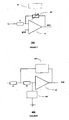
- Figure 7 shows a programmable gain amplifier 700 having an input connected to a terminal of resistor R1.
- a second terminal of resistor R1 may be coupled to a first input of amplifier 70 and a first terminal of a differential thermometric admittance circuit 300'.
- a second terminal of a differential thermometric admittance circuit 300" may be coupled to an output of the amplifier 70.
- a second input of amplifier 70 may be connected to a reference voltage which may be a ground potential.
- Control Inputs of differential thermometric admittance circuit 300' may be connected to a controller 60'.
- the admittance elements in admittance circuit 300' may be resistors and the switches may be implemented as MOS transistors having the gates connected to the controller 60'.In operation the controller 60' may switch the switchable admittance elements to vary the gain of the variable gain amplifier 700 by incrementing or decrementing the admittance value according to one of the control sequences previously described. Controller 60' may be implemented as a software programmable register and the control sequence may be implemented In software.
- control sequence may be Implemented using logic gates in hardware.
- the resistors may have a minimum value of 77 Ohms and a maximum value of 500 Ohms corresponding to an admittance varying between 2mS and 13 mS.
- the programmable gain amplifier may have a gain varying in steps of less than 0.2dB by incrementing or decrementing the admittance values.
- Figure 8 shows a programmable low pass filter 800.
- An input may be connected to a first terminal of resistor R2.
- a second terminal of resistor R2 may be connected to a first terminal of R3.
- a second terminal of R3 may be connected to an input of amplifier 80 and a first terminal of differential thermometric circuit 500".
- a second terminal of differential thermometric circuit 500' may be connected to a reference voltage which may be a ground.
- the second terminal of resistor R2 may be connected to first terminal of a differential thermometric circuit 500'.
- a second terminal of differential thermometric circuit 500" may be connected to an output of amplifier 80.
- the differential thermometric circuits 500' and 500" may use capacitors as admittance elements so can be used to adjust the frequency response characteristics of the filter.
- Embodiments may include a programmable resistor, capacitor, inductor, current source or transconductance with a fine step and over a wide range.
- Other embodiments may include an arrangement of serial impedances having an equivalent circuit of the parallel admittance circuits described herein.
Landscapes
- Engineering & Computer Science (AREA)
- Computer Hardware Design (AREA)
- Microelectronics & Electronic Packaging (AREA)
- Networks Using Active Elements (AREA)
- Semiconductor Integrated Circuits (AREA)
Claims (14)
- Circuit à admittance variable (500) comprenant une pluralité d'éléments à admittance agencés dans des branches parallèles, la pluralité d'éléments à admittance comprenant :un élément à admittance fixe (Y0) possédant une valeur d'admittance Y0,une séquence d'au moins trois éléments à admittance commutables (Y1, Y2 ... Yn) possédant des valeurs d'admittance respectives Y1 formant une séquence géométrique avec un rapport commun r et une première valeur Y1 donnée par
 le circuit à admittance variable étant apte à faire varier pas à pas l'admittance totale entre une valeur d'admittance minimale Ymin et une valeur d'admittance maximale Ymax en commutant les éléments à admittance commutables de manière à sélectionner ou à désélectionner les éléments à admittance commutables, etle rapport commun étant inférieur à deux et supérieur à un pas maximal, etlesdits au moins trois éléments à admittance commutables comprenant un premier élément à admittance commutable (Y1) possédant une valeur d'admittance Y1, un deuxième élément à admittance commutable (Y2) possédant une valeur d'admittance Y2 et un élément à admittance commutable additionnel de rang i (Yi) possédant une valeur d'admittance de K*(Y1+Y2), K étant un nombre compris entre 0,8 et 1,05.
 - Circuit à admittance variable selon la revendication 1, dans lequel, pour une branche 1 possédant une valeur supérieure au rang i, l'admittance de l'élément à admittance Y1 vaut K*(Yl-i+1+Yl-i+2), et lequel circuit à admittance variable est apte à accroître l'admittance totale d'une valeur de Yl-Yl-1 en désélectionnant l'élément à admittance commutable Yl-1, sélectionnant l'élément à admittance commutable Yl-i+1 et sélectionnant l'élément à admittance commutable Yl-i+2.
- Circuit à admittance variable selon l'une quelconque des revendications précédentes, comprenant en outre une unité de commande (60) couplée à chacun des éléments à admittance commutables, l'unité de commande étant configurée pour faire varier l'admittance totale entre la valeur d'admittance minimale Ymin et la valeur d'admittance maximale Ymax en commutant un maximum de trois éléments à admittance commutables.
- Circuit à admittance variable selon l'une quelconque des revendications précédentes, dans lequel le nombre de branches parallèles est supérieur ou égal à 2+log(Ymax/Ymin)/log(r).
- Circuit à admittance variable selon l'une quelconque des revendications précédentes, dans lequel au moins un des éléments à admittance comprend un condensateur.
- Circuit à admittance variable selon l'une quelconque des revendications précédentes, dans lequel au moins un des éléments à admittance comprend une résistance.
- Circuit à admittance variable selon l'une quelconque des revendications précédentes, dans lequel au moins un des éléments à admittance comprend une inductance.
- Circuit à admittance variable selon l'une quelconque des revendications précédentes, dans lequel au moins un des éléments à admittance comprend un transistor.
- Circuit à admittance variable selon l'une quelconque des revendications précédentes, dans lequel l'élément à admittance commutable comprend :un transistor possédant une borne de commande, une première borne de transistor et une deuxième borne de transistor,un élément à admittance possédant une première borne couplée à la première borne de transistor et une borne additionnelle, l'élément à admittance commutable étant apte à être commuté par application d'une tension de commande à la borne de commande du transistor.
- Filtre comprenant un amplificateur opérationnel couplé au circuit à admittance variable selon l'une quelconque des revendications précédentes.
- Amplificateur programmable comprenant un amplificateur opérationnel couplé au circuit à admittance variable selon l'une quelconque des revendications précédentes.
- Circuit syntoniseur radiofréquence comprenant le circuit à admittance variable selon l'une quelconque des revendications 1 à 9.
- Syntoniseur au silicium comprenant le circuit à admittance variable selon l'une quelconque des revendications 1 à 9.
- Procédé pour modifier l'admittance d'un circuit à admittance variable, le circuit à admittance variable comprenant une pluralité d'éléments à admittance agencés dans des branches parallèles, la pluralité d'éléments à admittance comprenant un élément à admittance fixe (Y0) possédant une valeur d'admittance Y0 et une séquence d'au moins trois éléments à admittance commutables (Y1, Y2 ... Yn) possédant des valeurs d'admittance respectives Y1, 1 étant un entier, le procédé comprenant les étapes consistant, pour des branches où 1 est supérieur ou égal à une valeur entière de rang prédéfinie i, à :sélectionner une branche d'une valeur d'admittance Y1+1, etaccroître l'admittance totale d'une valeur inférieure à Y1+1-Y1-1 en (1) si les branches possédant une valeur de Y1-i+1 et Y1-i+2 sont désélectionnées, désélectionnant l'élément à admittance commutable possédant une valeur Y1-1, sélectionnant l'élément à admittance commutable possédant une valeur Y1-i+1 et sélectionnant l'élément à admittance commutable possédant une valeur Y1-i+2, et (2) si les branches possédant une valeur de Y1-i+1 et Y1-i+2 sont déjà sélectionnées, désélectionnant l'élément à admittance commutable possédant une valeur Y1-1 et sélectionnant l'élément à admittance commutable possédant une valeur Y1.
Priority Applications (2)
| Application Number | Priority Date | Filing Date | Title |
|---|---|---|---|
| EP20130290044 EP2775615B1 (fr) | 2013-03-06 | 2013-03-06 | Circuit d'admittance variable |
| US14/195,710 US8963629B2 (en) | 2013-03-06 | 2014-03-03 | Variable admittance circuit |
Applications Claiming Priority (1)
| Application Number | Priority Date | Filing Date | Title |
|---|---|---|---|
| EP20130290044 EP2775615B1 (fr) | 2013-03-06 | 2013-03-06 | Circuit d'admittance variable |
Publications (2)
| Publication Number | Publication Date |
|---|---|
| EP2775615A1 EP2775615A1 (fr) | 2014-09-10 |
| EP2775615B1 true EP2775615B1 (fr) | 2015-05-13 |
Family
ID=48050622
Family Applications (1)
| Application Number | Title | Priority Date | Filing Date |
|---|---|---|---|
| EP20130290044 Not-in-force EP2775615B1 (fr) | 2013-03-06 | 2013-03-06 | Circuit d'admittance variable |
Country Status (2)
| Country | Link |
|---|---|
| US (1) | US8963629B2 (fr) |
| EP (1) | EP2775615B1 (fr) |
Families Citing this family (1)
| Publication number | Priority date | Publication date | Assignee | Title |
|---|---|---|---|---|
| US10790307B2 (en) | 2018-11-27 | 2020-09-29 | Qorvo Us, Inc. | Switch branch structure |
Family Cites Families (13)
| Publication number | Priority date | Publication date | Assignee | Title |
|---|---|---|---|---|
| DE19738718A1 (de) * | 1997-09-04 | 1999-03-25 | Siemens Ag | Oszillatorschaltung mit einem Schwingquarz |
| JP3114680B2 (ja) * | 1997-12-15 | 2000-12-04 | 日本電気株式会社 | アクティブフィルタ |
| US6424209B1 (en) * | 2000-02-18 | 2002-07-23 | Lattice Semiconductor Corporation | Integrated programmable continuous time filter with programmable capacitor arrays |
| US6563390B1 (en) * | 2000-12-29 | 2003-05-13 | Cypress Semiconductor Corp. | Digitally compensated voltage controlled oscillator |
| US6747522B2 (en) * | 2002-05-03 | 2004-06-08 | Silicon Laboratories, Inc. | Digitally controlled crystal oscillator with integrated coarse and fine control |
| US7050781B2 (en) | 2002-05-16 | 2006-05-23 | Intel Corporation | Self-calibrating tunable filter |
| US20050118990A1 (en) * | 2003-12-02 | 2005-06-02 | Sony Ericsson Mobile Communications Ab | Method for audible control of a camera |
| US7098738B2 (en) | 2003-12-24 | 2006-08-29 | Broadcom Corporation | Fine step and large gain range programmable gain amplifier |
| US7646236B2 (en) * | 2006-04-07 | 2010-01-12 | Qualcomm Incorporated | Method and apparatus for tuning resistors and capacitors |
| US20080100374A1 (en) * | 2006-10-30 | 2008-05-01 | Theta Microelectronics, Inc. | Programmable filters and methods of operation thereof |
| US8692612B2 (en) * | 2009-09-29 | 2014-04-08 | Stmicroelectronics S.R.L. | Electronic device for regulating a variable capacitance of an integrated circuit |
| US8154356B2 (en) * | 2009-12-19 | 2012-04-10 | Infineon Technologies Ag | Oscillator with capacitance array |
| US8816762B2 (en) * | 2010-01-13 | 2014-08-26 | Maxlinear, Inc. | Area-optimized analog filter with bandwidth control by a quantized scaling function |
-
2013
- 2013-03-06 EP EP20130290044 patent/EP2775615B1/fr not_active Not-in-force
-
2014
- 2014-03-03 US US14/195,710 patent/US8963629B2/en active Active
Also Published As
| Publication number | Publication date |
|---|---|
| US8963629B2 (en) | 2015-02-24 |
| US20140312965A1 (en) | 2014-10-23 |
| EP2775615A1 (fr) | 2014-09-10 |
Similar Documents
| Publication | Publication Date | Title |
|---|---|---|
| KR101663899B1 (ko) | 스위칭가능한 커패시턴스를 위한 시스템 및 방법 | |
| US6714066B2 (en) | Integrated programmable continuous time filter with programmable capacitor arrays | |
| EP2337219A1 (fr) | Atténuateur numérique à faible variation de phase | |
| CN101675487B (zh) | 可数控的片上电阻器及方法 | |
| KR20160131926A (ko) | 무선 주파수 스위치를 구동하기 위한 시스템 및 방법 | |
| US9876480B2 (en) | System and method for a tunable capacitance circuit | |
| KR101659651B1 (ko) | 스위칭 가능한 캐패시턴스를 위한 시스템 및 방법 | |
| US6937179B1 (en) | Resistor tuning network and method for tuning a resistor in an electronic circuit | |
| US9627882B2 (en) | Serial capacitance tuner | |
| US8638156B2 (en) | Multi-output-resistance switch driver circuits | |
| US11973480B2 (en) | Variable capacitance circuit and wireless communication device | |
| US6344780B1 (en) | Impedance adjusting circuit | |
| JP4214710B2 (ja) | 可変減衰器 | |
| EP2775615B1 (fr) | Circuit d'admittance variable | |
| EP3424147B1 (fr) | Oscillateur rc variable | |
| JP2010219941A (ja) | 高周波フィルタ | |
| CN112202420B (zh) | 一种可编程电容基本电路单元以及基于该电路单元并联和串联的电容选调电路 | |
| US20210083661A1 (en) | Variable capacitance circuit | |
| US20070187804A1 (en) | Monolithic integrated circuit | |
| EP2215719B1 (fr) | Composants électroniques intégrés appariés | |
| JPH1155059A (ja) | 可変減衰器 | |
| US12095435B2 (en) | High frequency variable attenuation circuit | |
| CN120415371B (zh) | 移相电路及移相电路系统 | |
| EP4407869A1 (fr) | Atténuateur numérique à gradins avec un circuit de dérivation pour un signal haute fréquence | |
| CN110198161B (zh) | 一种基于选择网络的片上时延线 |
Legal Events
| Date | Code | Title | Description |
|---|---|---|---|
| PUAI | Public reference made under article 153(3) epc to a published international application that has entered the european phase |
Free format text: ORIGINAL CODE: 0009012 |
|
| 17P | Request for examination filed |
Effective date: 20130829 |
|
| AK | Designated contracting states |
Kind code of ref document: A1 Designated state(s): AL AT BE BG CH CY CZ DE DK EE ES FI FR GB GR HR HU IE IS IT LI LT LU LV MC MK MT NL NO PL PT RO RS SE SI SK SM TR |
|
| AX | Request for extension of the european patent |
Extension state: BA ME |
|
| GRAP | Despatch of communication of intention to grant a patent |
Free format text: ORIGINAL CODE: EPIDOSNIGR1 |
|
| INTG | Intention to grant announced |
Effective date: 20141114 |
|
| REG | Reference to a national code |
Ref country code: DE Ref legal event code: R079 Ref document number: 602013001754 Country of ref document: DE Free format text: PREVIOUS MAIN CLASS: H03J0001000000 Ipc: H03H0011280000 |
|
| GRAP | Despatch of communication of intention to grant a patent |
Free format text: ORIGINAL CODE: EPIDOSNIGR1 |
|
| GRAS | Grant fee paid |
Free format text: ORIGINAL CODE: EPIDOSNIGR3 |
|
| RBV | Designated contracting states (corrected) |
Designated state(s): AL AT BE BG CH CY CZ DE DK EE ES FI FR GB GR HR HU IE IS IT LI LT LU LV MC MK MT NL NO PL PT RO RS SE SI SK SM TR |
|
| RIC1 | Information provided on ipc code assigned before grant |
Ipc: H03H 11/28 20060101AFI20150310BHEP Ipc: H03J 1/00 20060101ALI20150310BHEP |
|
| GRAA | (expected) grant |
Free format text: ORIGINAL CODE: 0009210 |
|
| INTG | Intention to grant announced |
Effective date: 20150323 |
|
| AK | Designated contracting states |
Kind code of ref document: B1 Designated state(s): AL AT BE BG CH CY CZ DE DK EE ES FI FR GB GR HR HU IE IS IT LI LT LU LV MC MK MT NL NO PL PT RO RS SE SI SK SM TR |
|
| REG | Reference to a national code |
Ref country code: GB Ref legal event code: FG4D |
|
| REG | Reference to a national code |
Ref country code: CH Ref legal event code: EP |
|
| REG | Reference to a national code |
Ref country code: IE Ref legal event code: FG4D |
|
| REG | Reference to a national code |
Ref country code: AT Ref legal event code: REF Ref document number: 727142 Country of ref document: AT Kind code of ref document: T Effective date: 20150615 |
|
| REG | Reference to a national code |
Ref country code: DE Ref legal event code: R096 Ref document number: 602013001754 Country of ref document: DE Effective date: 20150625 |
|
| REG | Reference to a national code |
Ref country code: AT Ref legal event code: MK05 Ref document number: 727142 Country of ref document: AT Kind code of ref document: T Effective date: 20150513 |
|
| REG | Reference to a national code |
Ref country code: NL Ref legal event code: MP Effective date: 20150513 |
|
| REG | Reference to a national code |
Ref country code: LT Ref legal event code: MG4D |
|
| PG25 | Lapsed in a contracting state [announced via postgrant information from national office to epo] |
Ref country code: PT Free format text: LAPSE BECAUSE OF FAILURE TO SUBMIT A TRANSLATION OF THE DESCRIPTION OR TO PAY THE FEE WITHIN THE PRESCRIBED TIME-LIMIT Effective date: 20150914 Ref country code: LT Free format text: LAPSE BECAUSE OF FAILURE TO SUBMIT A TRANSLATION OF THE DESCRIPTION OR TO PAY THE FEE WITHIN THE PRESCRIBED TIME-LIMIT Effective date: 20150513 Ref country code: NO Free format text: LAPSE BECAUSE OF FAILURE TO SUBMIT A TRANSLATION OF THE DESCRIPTION OR TO PAY THE FEE WITHIN THE PRESCRIBED TIME-LIMIT Effective date: 20150813 Ref country code: HR Free format text: LAPSE BECAUSE OF FAILURE TO SUBMIT A TRANSLATION OF THE DESCRIPTION OR TO PAY THE FEE WITHIN THE PRESCRIBED TIME-LIMIT Effective date: 20150513 Ref country code: FI Free format text: LAPSE BECAUSE OF FAILURE TO SUBMIT A TRANSLATION OF THE DESCRIPTION OR TO PAY THE FEE WITHIN THE PRESCRIBED TIME-LIMIT Effective date: 20150513 Ref country code: ES Free format text: LAPSE BECAUSE OF FAILURE TO SUBMIT A TRANSLATION OF THE DESCRIPTION OR TO PAY THE FEE WITHIN THE PRESCRIBED TIME-LIMIT Effective date: 20150513 |
|
| PG25 | Lapsed in a contracting state [announced via postgrant information from national office to epo] |
Ref country code: AT Free format text: LAPSE BECAUSE OF FAILURE TO SUBMIT A TRANSLATION OF THE DESCRIPTION OR TO PAY THE FEE WITHIN THE PRESCRIBED TIME-LIMIT Effective date: 20150513 Ref country code: LV Free format text: LAPSE BECAUSE OF FAILURE TO SUBMIT A TRANSLATION OF THE DESCRIPTION OR TO PAY THE FEE WITHIN THE PRESCRIBED TIME-LIMIT Effective date: 20150513 Ref country code: GR Free format text: LAPSE BECAUSE OF FAILURE TO SUBMIT A TRANSLATION OF THE DESCRIPTION OR TO PAY THE FEE WITHIN THE PRESCRIBED TIME-LIMIT Effective date: 20150814 Ref country code: BG Free format text: LAPSE BECAUSE OF FAILURE TO SUBMIT A TRANSLATION OF THE DESCRIPTION OR TO PAY THE FEE WITHIN THE PRESCRIBED TIME-LIMIT Effective date: 20150813 Ref country code: IS Free format text: LAPSE BECAUSE OF FAILURE TO SUBMIT A TRANSLATION OF THE DESCRIPTION OR TO PAY THE FEE WITHIN THE PRESCRIBED TIME-LIMIT Effective date: 20150913 Ref country code: RS Free format text: LAPSE BECAUSE OF FAILURE TO SUBMIT A TRANSLATION OF THE DESCRIPTION OR TO PAY THE FEE WITHIN THE PRESCRIBED TIME-LIMIT Effective date: 20150513 |
|
| PG25 | Lapsed in a contracting state [announced via postgrant information from national office to epo] |
Ref country code: DK Free format text: LAPSE BECAUSE OF FAILURE TO SUBMIT A TRANSLATION OF THE DESCRIPTION OR TO PAY THE FEE WITHIN THE PRESCRIBED TIME-LIMIT Effective date: 20150513 Ref country code: EE Free format text: LAPSE BECAUSE OF FAILURE TO SUBMIT A TRANSLATION OF THE DESCRIPTION OR TO PAY THE FEE WITHIN THE PRESCRIBED TIME-LIMIT Effective date: 20150513 |
|
| REG | Reference to a national code |
Ref country code: DE Ref legal event code: R097 Ref document number: 602013001754 Country of ref document: DE |
|
| REG | Reference to a national code |
Ref country code: FR Ref legal event code: PLFP Year of fee payment: 4 |
|
| PG25 | Lapsed in a contracting state [announced via postgrant information from national office to epo] |
Ref country code: SK Free format text: LAPSE BECAUSE OF FAILURE TO SUBMIT A TRANSLATION OF THE DESCRIPTION OR TO PAY THE FEE WITHIN THE PRESCRIBED TIME-LIMIT Effective date: 20150513 Ref country code: RO Free format text: LAPSE BECAUSE OF NON-PAYMENT OF DUE FEES Effective date: 20150513 Ref country code: PL Free format text: LAPSE BECAUSE OF FAILURE TO SUBMIT A TRANSLATION OF THE DESCRIPTION OR TO PAY THE FEE WITHIN THE PRESCRIBED TIME-LIMIT Effective date: 20150513 Ref country code: CZ Free format text: LAPSE BECAUSE OF FAILURE TO SUBMIT A TRANSLATION OF THE DESCRIPTION OR TO PAY THE FEE WITHIN THE PRESCRIBED TIME-LIMIT Effective date: 20150513 |
|
| PLBE | No opposition filed within time limit |
Free format text: ORIGINAL CODE: 0009261 |
|
| STAA | Information on the status of an ep patent application or granted ep patent |
Free format text: STATUS: NO OPPOSITION FILED WITHIN TIME LIMIT |
|
| 26N | No opposition filed |
Effective date: 20160216 |
|
| PG25 | Lapsed in a contracting state [announced via postgrant information from national office to epo] |
Ref country code: IT Free format text: LAPSE BECAUSE OF FAILURE TO SUBMIT A TRANSLATION OF THE DESCRIPTION OR TO PAY THE FEE WITHIN THE PRESCRIBED TIME-LIMIT Effective date: 20150513 |
|
| PG25 | Lapsed in a contracting state [announced via postgrant information from national office to epo] |
Ref country code: SI Free format text: LAPSE BECAUSE OF FAILURE TO SUBMIT A TRANSLATION OF THE DESCRIPTION OR TO PAY THE FEE WITHIN THE PRESCRIBED TIME-LIMIT Effective date: 20150513 |
|
| PG25 | Lapsed in a contracting state [announced via postgrant information from national office to epo] |
Ref country code: BE Free format text: LAPSE BECAUSE OF FAILURE TO SUBMIT A TRANSLATION OF THE DESCRIPTION OR TO PAY THE FEE WITHIN THE PRESCRIBED TIME-LIMIT Effective date: 20150513 |
|
| PG25 | Lapsed in a contracting state [announced via postgrant information from national office to epo] |
Ref country code: MC Free format text: LAPSE BECAUSE OF FAILURE TO SUBMIT A TRANSLATION OF THE DESCRIPTION OR TO PAY THE FEE WITHIN THE PRESCRIBED TIME-LIMIT Effective date: 20150513 Ref country code: LU Free format text: LAPSE BECAUSE OF FAILURE TO SUBMIT A TRANSLATION OF THE DESCRIPTION OR TO PAY THE FEE WITHIN THE PRESCRIBED TIME-LIMIT Effective date: 20160306 |
|
| REG | Reference to a national code |
Ref country code: CH Ref legal event code: PL |
|
| REG | Reference to a national code |
Ref country code: IE Ref legal event code: MM4A |
|
| PG25 | Lapsed in a contracting state [announced via postgrant information from national office to epo] |
Ref country code: LI Free format text: LAPSE BECAUSE OF NON-PAYMENT OF DUE FEES Effective date: 20160331 Ref country code: CH Free format text: LAPSE BECAUSE OF NON-PAYMENT OF DUE FEES Effective date: 20160331 Ref country code: IE Free format text: LAPSE BECAUSE OF NON-PAYMENT OF DUE FEES Effective date: 20160306 |
|
| REG | Reference to a national code |
Ref country code: FR Ref legal event code: PLFP Year of fee payment: 5 |
|
| PG25 | Lapsed in a contracting state [announced via postgrant information from national office to epo] |
Ref country code: SE Free format text: LAPSE BECAUSE OF FAILURE TO SUBMIT A TRANSLATION OF THE DESCRIPTION OR TO PAY THE FEE WITHIN THE PRESCRIBED TIME-LIMIT Effective date: 20150513 Ref country code: NL Free format text: LAPSE BECAUSE OF FAILURE TO SUBMIT A TRANSLATION OF THE DESCRIPTION OR TO PAY THE FEE WITHIN THE PRESCRIBED TIME-LIMIT Effective date: 20150513 |
|
| PG25 | Lapsed in a contracting state [announced via postgrant information from national office to epo] |
Ref country code: MT Free format text: LAPSE BECAUSE OF FAILURE TO SUBMIT A TRANSLATION OF THE DESCRIPTION OR TO PAY THE FEE WITHIN THE PRESCRIBED TIME-LIMIT Effective date: 20150513 |
|
| GBPC | Gb: european patent ceased through non-payment of renewal fee |
Effective date: 20170306 |
|
| REG | Reference to a national code |
Ref country code: FR Ref legal event code: PLFP Year of fee payment: 6 |
|
| PG25 | Lapsed in a contracting state [announced via postgrant information from national office to epo] |
Ref country code: GB Free format text: LAPSE BECAUSE OF NON-PAYMENT OF DUE FEES Effective date: 20170306 |
|
| PG25 | Lapsed in a contracting state [announced via postgrant information from national office to epo] |
Ref country code: HU Free format text: LAPSE BECAUSE OF FAILURE TO SUBMIT A TRANSLATION OF THE DESCRIPTION OR TO PAY THE FEE WITHIN THE PRESCRIBED TIME-LIMIT; INVALID AB INITIO Effective date: 20130306 Ref country code: SM Free format text: LAPSE BECAUSE OF FAILURE TO SUBMIT A TRANSLATION OF THE DESCRIPTION OR TO PAY THE FEE WITHIN THE PRESCRIBED TIME-LIMIT Effective date: 20150513 |
|
| PG25 | Lapsed in a contracting state [announced via postgrant information from national office to epo] |
Ref country code: TR Free format text: LAPSE BECAUSE OF FAILURE TO SUBMIT A TRANSLATION OF THE DESCRIPTION OR TO PAY THE FEE WITHIN THE PRESCRIBED TIME-LIMIT Effective date: 20150513 Ref country code: MK Free format text: LAPSE BECAUSE OF FAILURE TO SUBMIT A TRANSLATION OF THE DESCRIPTION OR TO PAY THE FEE WITHIN THE PRESCRIBED TIME-LIMIT Effective date: 20150513 Ref country code: CY Free format text: LAPSE BECAUSE OF FAILURE TO SUBMIT A TRANSLATION OF THE DESCRIPTION OR TO PAY THE FEE WITHIN THE PRESCRIBED TIME-LIMIT Effective date: 20150513 Ref country code: MT Free format text: LAPSE BECAUSE OF FAILURE TO SUBMIT A TRANSLATION OF THE DESCRIPTION OR TO PAY THE FEE WITHIN THE PRESCRIBED TIME-LIMIT Effective date: 20160331 |
|
| PG25 | Lapsed in a contracting state [announced via postgrant information from national office to epo] |
Ref country code: AL Free format text: LAPSE BECAUSE OF FAILURE TO SUBMIT A TRANSLATION OF THE DESCRIPTION OR TO PAY THE FEE WITHIN THE PRESCRIBED TIME-LIMIT Effective date: 20150513 |
|
| PGFP | Annual fee paid to national office [announced via postgrant information from national office to epo] |
Ref country code: DE Payment date: 20190219 Year of fee payment: 7 |
|
| PGFP | Annual fee paid to national office [announced via postgrant information from national office to epo] |
Ref country code: FR Payment date: 20190220 Year of fee payment: 7 |
|
| REG | Reference to a national code |
Ref country code: DE Ref legal event code: R119 Ref document number: 602013001754 Country of ref document: DE |
|
| PG25 | Lapsed in a contracting state [announced via postgrant information from national office to epo] |
Ref country code: DE Free format text: LAPSE BECAUSE OF NON-PAYMENT OF DUE FEES Effective date: 20201001 Ref country code: FR Free format text: LAPSE BECAUSE OF NON-PAYMENT OF DUE FEES Effective date: 20200331 |