EP2784838A1 - Piezoelektrisches/elektrostriktives Element - Google Patents
Piezoelektrisches/elektrostriktives Element Download PDFInfo
- Publication number
- EP2784838A1 EP2784838A1 EP14159738.5A EP14159738A EP2784838A1 EP 2784838 A1 EP2784838 A1 EP 2784838A1 EP 14159738 A EP14159738 A EP 14159738A EP 2784838 A1 EP2784838 A1 EP 2784838A1
- Authority
- EP
- European Patent Office
- Prior art keywords
- electrode
- piezoelectric body
- glass layer
- piezoelectric
- sample
- Prior art date
- Legal status (The legal status is an assumption and is not a legal conclusion. Google has not performed a legal analysis and makes no representation as to the accuracy of the status listed.)
- Withdrawn
Links
- 239000011521 glass Substances 0.000 claims abstract description 93
- 238000009751 slip forming Methods 0.000 claims abstract description 7
- 239000000470 constituent Substances 0.000 claims abstract description 3
- 238000000034 method Methods 0.000 description 23
- 238000006073 displacement reaction Methods 0.000 description 22
- 229920002120 photoresistant polymer Polymers 0.000 description 22
- 239000010931 gold Substances 0.000 description 18
- 239000000758 substrate Substances 0.000 description 18
- 239000000463 material Substances 0.000 description 16
- 239000007788 liquid Substances 0.000 description 15
- 230000001681 protective effect Effects 0.000 description 13
- 239000007921 spray Substances 0.000 description 12
- 238000005530 etching Methods 0.000 description 10
- 239000004020 conductor Substances 0.000 description 9
- BASFCYQUMIYNBI-UHFFFAOYSA-N platinum Chemical compound [Pt] BASFCYQUMIYNBI-UHFFFAOYSA-N 0.000 description 8
- 230000005684 electric field Effects 0.000 description 7
- 239000000843 powder Substances 0.000 description 7
- 238000010304 firing Methods 0.000 description 6
- 230000008602 contraction Effects 0.000 description 5
- 230000000694 effects Effects 0.000 description 5
- 230000002401 inhibitory effect Effects 0.000 description 5
- 238000004519 manufacturing process Methods 0.000 description 5
- 239000000203 mixture Substances 0.000 description 5
- 238000012545 processing Methods 0.000 description 5
- KDLHZDBZIXYQEI-UHFFFAOYSA-N Palladium Chemical compound [Pd] KDLHZDBZIXYQEI-UHFFFAOYSA-N 0.000 description 4
- 230000015572 biosynthetic process Effects 0.000 description 4
- WMWLMWRWZQELOS-UHFFFAOYSA-N bismuth(iii) oxide Chemical compound O=[Bi]O[Bi]=O WMWLMWRWZQELOS-UHFFFAOYSA-N 0.000 description 4
- 239000007772 electrode material Substances 0.000 description 4
- 239000011810 insulating material Substances 0.000 description 4
- 229910000510 noble metal Inorganic materials 0.000 description 4
- 238000000206 photolithography Methods 0.000 description 4
- 230000010287 polarization Effects 0.000 description 4
- 230000009467 reduction Effects 0.000 description 4
- DDFHBQSCUXNBSA-UHFFFAOYSA-N 5-(5-carboxythiophen-2-yl)thiophene-2-carboxylic acid Chemical compound S1C(C(=O)O)=CC=C1C1=CC=C(C(O)=O)S1 DDFHBQSCUXNBSA-UHFFFAOYSA-N 0.000 description 3
- VEXZGXHMUGYJMC-UHFFFAOYSA-N Hydrochloric acid Chemical compound Cl VEXZGXHMUGYJMC-UHFFFAOYSA-N 0.000 description 3
- VYPSYNLAJGMNEJ-UHFFFAOYSA-N Silicium dioxide Chemical compound O=[Si]=O VYPSYNLAJGMNEJ-UHFFFAOYSA-N 0.000 description 3
- 239000011230 binding agent Substances 0.000 description 3
- 229910000416 bismuth oxide Inorganic materials 0.000 description 3
- 229910052810 boron oxide Inorganic materials 0.000 description 3
- 239000008139 complexing agent Substances 0.000 description 3
- TYIXMATWDRGMPF-UHFFFAOYSA-N dibismuth;oxygen(2-) Chemical compound [O-2].[O-2].[O-2].[Bi+3].[Bi+3] TYIXMATWDRGMPF-UHFFFAOYSA-N 0.000 description 3
- JKWMSGQKBLHBQQ-UHFFFAOYSA-N diboron trioxide Chemical compound O=BOB=O JKWMSGQKBLHBQQ-UHFFFAOYSA-N 0.000 description 3
- 239000002270 dispersing agent Substances 0.000 description 3
- 238000005516 engineering process Methods 0.000 description 3
- 238000011156 evaluation Methods 0.000 description 3
- 230000005764 inhibitory process Effects 0.000 description 3
- 229910052697 platinum Inorganic materials 0.000 description 3
- 230000002829 reductive effect Effects 0.000 description 3
- 239000011347 resin Substances 0.000 description 3
- 229920005989 resin Polymers 0.000 description 3
- 230000004044 response Effects 0.000 description 3
- 238000001878 scanning electron micrograph Methods 0.000 description 3
- 229910052814 silicon oxide Inorganic materials 0.000 description 3
- 239000002002 slurry Substances 0.000 description 3
- 239000000243 solution Substances 0.000 description 3
- 239000004094 surface-active agent Substances 0.000 description 3
- 239000002562 thickening agent Substances 0.000 description 3
- YCKRFDGAMUMZLT-UHFFFAOYSA-N Fluorine atom Chemical compound [F] YCKRFDGAMUMZLT-UHFFFAOYSA-N 0.000 description 2
- XLOMVQKBTHCTTD-UHFFFAOYSA-N Zinc monoxide Chemical compound [Zn]=O XLOMVQKBTHCTTD-UHFFFAOYSA-N 0.000 description 2
- 239000002253 acid Substances 0.000 description 2
- 230000003197 catalytic effect Effects 0.000 description 2
- 238000000576 coating method Methods 0.000 description 2
- 229920001940 conductive polymer Polymers 0.000 description 2
- 239000010949 copper Substances 0.000 description 2
- 239000012153 distilled water Substances 0.000 description 2
- 238000009713 electroplating Methods 0.000 description 2
- 229910052731 fluorine Inorganic materials 0.000 description 2
- 239000011737 fluorine Substances 0.000 description 2
- XMFOQHDPRMAJNU-UHFFFAOYSA-N lead(II,IV) oxide Inorganic materials O1[Pb]O[Pb]11O[Pb]O1 XMFOQHDPRMAJNU-UHFFFAOYSA-N 0.000 description 2
- 238000005259 measurement Methods 0.000 description 2
- 238000002156 mixing Methods 0.000 description 2
- TWNQGVIAIRXVLR-UHFFFAOYSA-N oxo(oxoalumanyloxy)alumane Chemical compound O=[Al]O[Al]=O TWNQGVIAIRXVLR-UHFFFAOYSA-N 0.000 description 2
- 229910052763 palladium Inorganic materials 0.000 description 2
- 230000008569 process Effects 0.000 description 2
- 238000007650 screen-printing Methods 0.000 description 2
- 238000005245 sintering Methods 0.000 description 2
- 238000012360 testing method Methods 0.000 description 2
- XLYOFNOQVPJJNP-UHFFFAOYSA-N water Chemical compound O XLYOFNOQVPJJNP-UHFFFAOYSA-N 0.000 description 2
- HXQQNYSFSLBXQJ-UHFFFAOYSA-N COC1=C(NC(CO)C(O)=O)CC(O)(CO)CC1=NCC(O)=O Chemical compound COC1=C(NC(CO)C(O)=O)CC(O)(CO)CC1=NCC(O)=O HXQQNYSFSLBXQJ-UHFFFAOYSA-N 0.000 description 1
- RYGMFSIKBFXOCR-UHFFFAOYSA-N Copper Chemical compound [Cu] RYGMFSIKBFXOCR-UHFFFAOYSA-N 0.000 description 1
- 229910052581 Si3N4 Inorganic materials 0.000 description 1
- BQCADISMDOOEFD-UHFFFAOYSA-N Silver Chemical compound [Ag] BQCADISMDOOEFD-UHFFFAOYSA-N 0.000 description 1
- GWEVSGVZZGPLCZ-UHFFFAOYSA-N Titan oxide Chemical compound O=[Ti]=O GWEVSGVZZGPLCZ-UHFFFAOYSA-N 0.000 description 1
- 230000001133 acceleration Effects 0.000 description 1
- 230000002378 acidificating effect Effects 0.000 description 1
- 229910045601 alloy Inorganic materials 0.000 description 1
- 239000000956 alloy Substances 0.000 description 1
- 239000007864 aqueous solution Substances 0.000 description 1
- 230000008901 benefit Effects 0.000 description 1
- BRPQOXSCLDDYGP-UHFFFAOYSA-N calcium oxide Chemical compound [O-2].[Ca+2] BRPQOXSCLDDYGP-UHFFFAOYSA-N 0.000 description 1
- 239000000292 calcium oxide Substances 0.000 description 1
- ODINCKMPIJJUCX-UHFFFAOYSA-N calcium oxide Inorganic materials [Ca]=O ODINCKMPIJJUCX-UHFFFAOYSA-N 0.000 description 1
- 239000003054 catalyst Substances 0.000 description 1
- 229910010293 ceramic material Inorganic materials 0.000 description 1
- 239000003795 chemical substances by application Substances 0.000 description 1
- 239000011248 coating agent Substances 0.000 description 1
- 150000001875 compounds Chemical class 0.000 description 1
- 229910052802 copper Inorganic materials 0.000 description 1
- PMHQVHHXPFUNSP-UHFFFAOYSA-M copper(1+);methylsulfanylmethane;bromide Chemical compound Br[Cu].CSC PMHQVHHXPFUNSP-UHFFFAOYSA-M 0.000 description 1
- 238000005238 degreasing Methods 0.000 description 1
- KZHJGOXRZJKJNY-UHFFFAOYSA-N dioxosilane;oxo(oxoalumanyloxy)alumane Chemical compound O=[Si]=O.O=[Si]=O.O=[Al]O[Al]=O.O=[Al]O[Al]=O.O=[Al]O[Al]=O KZHJGOXRZJKJNY-UHFFFAOYSA-N 0.000 description 1
- PCHJSUWPFVWCPO-UHFFFAOYSA-N gold Chemical compound [Au] PCHJSUWPFVWCPO-UHFFFAOYSA-N 0.000 description 1
- 229910052737 gold Inorganic materials 0.000 description 1
- 229910000765 intermetallic Inorganic materials 0.000 description 1
- 238000010030 laminating Methods 0.000 description 1
- HFGPZNIAWCZYJU-UHFFFAOYSA-N lead zirconate titanate Chemical compound [O-2].[O-2].[O-2].[O-2].[O-2].[Ti+4].[Zr+4].[Pb+2] HFGPZNIAWCZYJU-UHFFFAOYSA-N 0.000 description 1
- 239000000395 magnesium oxide Substances 0.000 description 1
- CPLXHLVBOLITMK-UHFFFAOYSA-N magnesium oxide Inorganic materials [Mg]=O CPLXHLVBOLITMK-UHFFFAOYSA-N 0.000 description 1
- AXZKOIWUVFPNLO-UHFFFAOYSA-N magnesium;oxygen(2-) Chemical compound [O-2].[Mg+2] AXZKOIWUVFPNLO-UHFFFAOYSA-N 0.000 description 1
- 238000012986 modification Methods 0.000 description 1
- 230000004048 modification Effects 0.000 description 1
- 229910052863 mullite Inorganic materials 0.000 description 1
- 230000010355 oscillation Effects 0.000 description 1
- RVTZCBVAJQQJTK-UHFFFAOYSA-N oxygen(2-);zirconium(4+) Chemical compound [O-2].[O-2].[Zr+4] RVTZCBVAJQQJTK-UHFFFAOYSA-N 0.000 description 1
- 229910002077 partially stabilized zirconia Inorganic materials 0.000 description 1
- 239000002245 particle Substances 0.000 description 1
- 238000000059 patterning Methods 0.000 description 1
- 229910001392 phosphorus oxide Inorganic materials 0.000 description 1
- 239000004014 plasticizer Substances 0.000 description 1
- 238000007639 printing Methods 0.000 description 1
- 230000000717 retained effect Effects 0.000 description 1
- 238000007789 sealing Methods 0.000 description 1
- HQVNEWCFYHHQES-UHFFFAOYSA-N silicon nitride Chemical compound N12[Si]34N5[Si]62N3[Si]51N64 HQVNEWCFYHHQES-UHFFFAOYSA-N 0.000 description 1
- 229910052709 silver Inorganic materials 0.000 description 1
- 239000004332 silver Substances 0.000 description 1
- VSAISIQCTGDGPU-UHFFFAOYSA-N tetraphosphorus hexaoxide Chemical compound O1P(O2)OP3OP1OP2O3 VSAISIQCTGDGPU-UHFFFAOYSA-N 0.000 description 1
- OGIDPMRJRNCKJF-UHFFFAOYSA-N titanium oxide Inorganic materials [Ti]=O OGIDPMRJRNCKJF-UHFFFAOYSA-N 0.000 description 1
- 239000011787 zinc oxide Substances 0.000 description 1
- 229910001928 zirconium oxide Inorganic materials 0.000 description 1
Images



Classifications
-
- B—PERFORMING OPERATIONS; TRANSPORTING
- B41—PRINTING; LINING MACHINES; TYPEWRITERS; STAMPS
- B41J—TYPEWRITERS; SELECTIVE PRINTING MECHANISMS, i.e. MECHANISMS PRINTING OTHERWISE THAN FROM A FORME; CORRECTION OF TYPOGRAPHICAL ERRORS
- B41J2/00—Typewriters or selective printing mechanisms characterised by the printing or marking process for which they are designed
- B41J2/005—Typewriters or selective printing mechanisms characterised by the printing or marking process for which they are designed characterised by bringing liquid or particles selectively into contact with a printing material
- B41J2/01—Ink jet
- B41J2/135—Nozzles
- B41J2/14—Structure thereof only for on-demand ink jet heads
- B41J2/14201—Structure of print heads with piezoelectric elements
- B41J2/14233—Structure of print heads with piezoelectric elements of film type, deformed by bending and disposed on a diaphragm
-
- B—PERFORMING OPERATIONS; TRANSPORTING
- B41—PRINTING; LINING MACHINES; TYPEWRITERS; STAMPS
- B41J—TYPEWRITERS; SELECTIVE PRINTING MECHANISMS, i.e. MECHANISMS PRINTING OTHERWISE THAN FROM A FORME; CORRECTION OF TYPOGRAPHICAL ERRORS
- B41J2/00—Typewriters or selective printing mechanisms characterised by the printing or marking process for which they are designed
- B41J2/005—Typewriters or selective printing mechanisms characterised by the printing or marking process for which they are designed characterised by bringing liquid or particles selectively into contact with a printing material
- B41J2/01—Ink jet
- B41J2/135—Nozzles
- B41J2/16—Production of nozzles
- B41J2/1607—Production of print heads with piezoelectric elements
- B41J2/161—Production of print heads with piezoelectric elements of film type, deformed by bending and disposed on a diaphragm
-
- B—PERFORMING OPERATIONS; TRANSPORTING
- B41—PRINTING; LINING MACHINES; TYPEWRITERS; STAMPS
- B41J—TYPEWRITERS; SELECTIVE PRINTING MECHANISMS, i.e. MECHANISMS PRINTING OTHERWISE THAN FROM A FORME; CORRECTION OF TYPOGRAPHICAL ERRORS
- B41J2/00—Typewriters or selective printing mechanisms characterised by the printing or marking process for which they are designed
- B41J2/005—Typewriters or selective printing mechanisms characterised by the printing or marking process for which they are designed characterised by bringing liquid or particles selectively into contact with a printing material
- B41J2/01—Ink jet
- B41J2/135—Nozzles
- B41J2/16—Production of nozzles
- B41J2/1621—Manufacturing processes
- B41J2/1626—Manufacturing processes etching
- B41J2/1629—Manufacturing processes etching wet etching
-
- B—PERFORMING OPERATIONS; TRANSPORTING
- B41—PRINTING; LINING MACHINES; TYPEWRITERS; STAMPS
- B41J—TYPEWRITERS; SELECTIVE PRINTING MECHANISMS, i.e. MECHANISMS PRINTING OTHERWISE THAN FROM A FORME; CORRECTION OF TYPOGRAPHICAL ERRORS
- B41J2/00—Typewriters or selective printing mechanisms characterised by the printing or marking process for which they are designed
- B41J2/005—Typewriters or selective printing mechanisms characterised by the printing or marking process for which they are designed characterised by bringing liquid or particles selectively into contact with a printing material
- B41J2/01—Ink jet
- B41J2/135—Nozzles
- B41J2/16—Production of nozzles
- B41J2/1621—Manufacturing processes
- B41J2/1631—Manufacturing processes photolithography
-
- B—PERFORMING OPERATIONS; TRANSPORTING
- B41—PRINTING; LINING MACHINES; TYPEWRITERS; STAMPS
- B41J—TYPEWRITERS; SELECTIVE PRINTING MECHANISMS, i.e. MECHANISMS PRINTING OTHERWISE THAN FROM A FORME; CORRECTION OF TYPOGRAPHICAL ERRORS
- B41J2/00—Typewriters or selective printing mechanisms characterised by the printing or marking process for which they are designed
- B41J2/005—Typewriters or selective printing mechanisms characterised by the printing or marking process for which they are designed characterised by bringing liquid or particles selectively into contact with a printing material
- B41J2/01—Ink jet
- B41J2/135—Nozzles
- B41J2/16—Production of nozzles
- B41J2/1621—Manufacturing processes
- B41J2/164—Manufacturing processes thin film formation
- B41J2/1645—Manufacturing processes thin film formation thin film formation by spincoating
-
- H—ELECTRICITY
- H10—SEMICONDUCTOR DEVICES; ELECTRIC SOLID-STATE DEVICES NOT OTHERWISE PROVIDED FOR
- H10N—ELECTRIC SOLID-STATE DEVICES NOT OTHERWISE PROVIDED FOR
- H10N30/00—Piezoelectric or electrostrictive devices
- H10N30/20—Piezoelectric or electrostrictive devices with electrical input and mechanical output, e.g. functioning as actuators or vibrators
- H10N30/204—Piezoelectric or electrostrictive devices with electrical input and mechanical output, e.g. functioning as actuators or vibrators using bending displacement, e.g. unimorph, bimorph or multimorph cantilever or membrane benders
- H10N30/2047—Membrane type
-
- H—ELECTRICITY
- H10—SEMICONDUCTOR DEVICES; ELECTRIC SOLID-STATE DEVICES NOT OTHERWISE PROVIDED FOR
- H10N—ELECTRIC SOLID-STATE DEVICES NOT OTHERWISE PROVIDED FOR
- H10N30/00—Piezoelectric or electrostrictive devices
- H10N30/704—Piezoelectric or electrostrictive devices based on piezoelectric or electrostrictive films or coatings
-
- H—ELECTRICITY
- H10—SEMICONDUCTOR DEVICES; ELECTRIC SOLID-STATE DEVICES NOT OTHERWISE PROVIDED FOR
- H10N—ELECTRIC SOLID-STATE DEVICES NOT OTHERWISE PROVIDED FOR
- H10N30/00—Piezoelectric or electrostrictive devices
- H10N30/80—Constructional details
- H10N30/87—Electrodes or interconnections, e.g. leads or terminals
Definitions
- the technology disclosed herein relates to a piezoelectric/electrostrictive element that has an electrode disposed on a piezoelectric body.
- Patent Literature 1 discloses a method of interposing a glass layer between an electrode and a piezoelectric body.
- Patent Literature 2 discloses a method of sealing an end portion of the electrode with a resin layer.
- the object of the technology disclosed herein is to provide a piezoelectric/electrostrictive element that enables inhibition of a reduction in the displacement of the piezoelectric body while inhibiting peeling of the electrode.
- a piezoelectric/electrostrictive element has a piezoelectric body, a first electrode, a second electrode and a glass layer.
- the piezoelectric body is formed in a thin film-shape.
- the piezoelectric body has a first main surface and a second main surface.
- the first electrode is disposed on the first main surface of the piezoelectric body.
- the first electrode has an electrode side surface configured to be connected with the first main surface.
- the second electrode is disposed on the second main surface of the piezoelectric body.
- the glass layer is continuously formed on the first main surface and the electrode side surface.
- the glass layer containing glass as a principal constituent.
- the glass layer is isolated from the side surface of the piezoelectric body.
- the technology disclosed herein provides a piezoelectric/electrostrictive element that enables inhibition of a reduction in the displacement of the piezoelectric body while inhibiting peeling of the electrode.
- the piezoelectric/electrostrictive element can be applied to various uses such as an oscillation circuit, various types of sensors or an injector actuator.
- FIG. 1 is a plan view illustrating a configuration of the actuator 100.
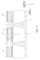
- FIG. 2 is a sectional view along the line X-X in FIG. 1 .
- FIG. 3 is an enlargement of a portion of FIG. 2 .
- the direction in which the piezoelectric/electrostrictive element 20 extends is termed the "length direction”
- the direction that is orthogonal to the length direction is termed the "width direction”.
- the direction that is orthogonal to the length direction and the width direction is termed the "thickness direction”.
- the actuator 100 includes a substrate 10 and a plurality of piezoelectric/electrostrictive elements 20.
- the substrate 10 is a plate-shaped fired body.
- the substrate 10 is configured from an insulating material.
- the insulating material used to configure the substrate 10 includes for example, stabilized zirconium oxide, aluminum oxide, magnesium oxide, mullite, aluminum nitride and silicon nitride, or the like.
- the insulating material that configures the substrate 10 is not limited to a ceramic material and may be configured by a glass material, a resin material, or the like. Furthermore, the particles that configure the substrate 10 may be a monocrystal, a polycrystal, or an amorphous material.
- the substrate 10 includes a diaphragm 11, a pressure chamber 12 and a discharge nozzle 13.
- the diaphragm 11 is a thin plate configured to support the piezoelectric/electrostrictive element 20.
- the diaphragm 11 vibrates (displaces) in the thickness direction in response to expansion and contraction of the piezoelectric/electrostrictive element 20.
- the pressure chamber 12 is a cavity provided below the diaphragm 11.
- the pressure chamber 12 retains ink injected from an ink guide port (not illustrated).
- the discharge nozzle 13 extends downwardly from the pressure chamber 12. The ink retained in the pressure chamber 12 is discharged from the discharge nozzle 13 in response to the vibration of the diaphragm 11.
- the piezoelectric/electrostrictive element 20 extends in the length direction on the substrate 10. A plurality of piezoelectric/electrostrictive elements 20 is mutually aligned in parallel.
- the piezoelectric/electrostrictive element 20 includes a lower electrode 21, a piezoelectric body 22, an upper electrode 23, and a glass layer 24.
- the upper electrode 23 is an example of "a first electrode”
- the lower electrode 21 is an example of "a second electrode”.
- the lower electrode 21 is a thin film-shaped fired body that is disposed on the diaphragm 11. When viewed in plan, the lower electrode 21 is formed with a size that is smaller than the size of the diaphragm 11.
- the length of the lower electrode 21 is for example 500 microns to 5000 microns.
- the width of the lower electrode 21 is for example 30 microns to 500 microns.
- the thickness of the lower electrode 21 is for example 0.1 microns to 10.0 microns.
- the lower electrode 21 is configured from an acid resistant conductive material.
- the conductive material includes for example noble metals such as platinum (Pt) or the like, in addition to conductive polymers and conductive oxides.
- the piezoelectric body 22 is a thin film-shaped fired body disposed on the lower electrode 21.
- the piezoelectric body 22 includes a first main surface 22S, a second main surface 22T, and a side surface 22U.
- the upper electrode 23 is disposed on the first main surface 22S.
- the lower electrode 21 is disposed on the second main surface 22T.
- the diaphragm 11 vibrates (displaces) in the thickness direction in response to the contraction or expansion of the piezoelectric body 22.
- the side surface 22U is connected to the first main surface 22S and the second main surface 22T. There is no requirement that the side surface 22U has a perpendicular configuration with respect to the first main surface 22S and the second main surface 22T.
- the piezoelectric body 22 is formed with a size that is smaller than or equal to the size of the lower electrode 21.
- the length of the piezoelectric body 22 is for example 500 microns to 5000 microns.
- the width of the piezoelectric body 22 is for example 30 microns to 500 microns.
- the thickness of the piezoelectric body 22 is for example 0.5 microns to 15.0 microns.
- the piezoelectric body 22 is formed with a size that is larger than the size of the upper electrode 23. As a result, the external edge portion of the first main surface 22S of the piezoelectric body 22 is exposed from the upper electrode 23.
- the piezoelectric body 22 is configured from a polycrystal piezoelectric material.
- the piezoelectric material includes for example lead titanate zirconate (PZT), or the like.
- the upper electrode 23 is a thin film-shaped fired body disposed on the piezoelectric body 22.
- the upper electrode 23 includes an electrode side surface 23S and an electrode upper surface 23T.
- the electrode side surface 23S is connected to the first main surface 22S of the piezoelectric body 22.
- the electrode side surface 23S may not be perpendicular with respect to the first main surface 22S, and may be inclined with respect to the first main surface 22S.
- the electrode upper surface 23T is connected to the electrode side surface 23S.
- the electrode upper surface 23T may not be perpendicular with respect to the electrode side surface 23S, and may be inclined with respect to the electrode side surface 23S.
- the upper electrode 23 is formed with a size that is smaller than the size of the piezoelectric body 22.
- the length of the upper electrode 23 is for example 498 microns to 4998 microns.
- the width of the upper electrode 23 is for example 28 microns to 498 microns.
- the thickness of the upper electrode 23 is for example 0.01 microns to 10.0 microns.
- the upper electrode 23 is configured from an acid resistant conductive material.
- the conductive material includes noble metals such as gold (Au), silver (Ag), platinum (Pt), or copper (Cu), or an alloy formed from such noble metals.
- the conductive material that configures the upper electrode 23 is not limited to a noble metal, and includes a conductive polymer or a conductive oxide.
- a material other than a conductive material may be added to the upper electrode 23.
- the conductive material may include a trace amount of the glass material that configures the glass layer 24.
- the glass layer 24 is formed and connected with the electrode side surface 23S of the upper electrode 23 and the first main surface 22S of the piezoelectric body 22. However, the glass layer 24 is not formed on the side surface 22U of the piezoelectric body 22, and is isolated from the side surface 22U.
- the glass layer 24 includes a bonding portion 241, a first extending portion 242, and a second extending portion 243.
- the bonding portion 241 is formed to cover the boundary P of the electrode side surface 23S and the first main surface 22S.
- the bonding portion 241 is continuously formed on the first main surface 22S and the electrode side surface 23S.
- the upper electrode 23 is bonded onto the piezoelectric body 22 by the connection formed by the bonding portion 241 between the first main surface 22S and the electrode side surface 23S. In this manner, the outer edge of the upper electrode 23 can be inhibited from peeling from the piezoelectric body 22.
- the first extending portion 242 is connected with the bonding portion 241 and extends onto the first main surface 22S.
- the first extending portion 242 extends only onto the first main surface 22S, and is not formed on the side surface 22U of the piezoelectric body 22.
- the second extending portion 243 is connected with the bonding portion 241 and extends onto the electrode side surface 23S.
- the second extending portion 243 extends only onto the electrode side surface 23S, and is not formed on the electrode upper surface 23T.
- the glass layer 24 contains at least one main component selected from the group consisting of bismuth oxide, boron oxide, silicon oxide, zinc oxide, aluminum oxide, phosphorus oxide, calcium oxide and titanium oxide.
- a composition X in which a substance Y is "contained as a main component" means that the material Y relative to the whole of the composition X is preferably at least 60 wt%, more preferably at least 70 wt%, and still more preferably at least 90 wt%.
- the glass layer 24 may be formed as a uniform layer, but also may be formed in a net-like structure.
- the strength of the glass layer 24 itself can be enhanced.
- the glass layer 24 is formed in a net-like structure, the effect on the expansion and contraction (displacement) of the piezoelectric body 22 can be reduced.
- a portion of the glass layer 24 may be formed in a layer structure, and the residual portion may be formed in a net-like structure.
- the thickness of the glass layer 24 may be for example 1 nm to 10 microns.
- the thickness of the glass layer 24 is preferably less than the thickness of the upper electrode 23. More specifically, the thickness of the glass layer 24 is preferably less than or equal to 30% of the thickness of the upper electrode 23. This is due to the fact that the effect of the rigidity of the glass layer 24 on the displacement of the diaphragm 11 is conspicuously reduced.
- a laminated body is prepared by laminating a plurality of green sheets that is configured by the insulating material used in the substrate 10. Each green sheets is punched into a predetermined pattern. The inner portion of the laminated body is formed into a cavity corresponding to the pressure chamber 12, the discharge nozzle 13.
- the substrate 10 is prepared by firing of the laminated body.
- a spin coat method or the like is used to coat a photoresist (negative resist) onto the substrate 10 and thereby form a photoresist film.
- the photoresist film is patterned by use of photolithography into a shape that corresponds to the lower electrode 21.
- a spray coat method or the like is used to coat a catalytic solution containing palladium for example onto openings of the photoresist film.
- an electroplating method or the like is used to form the lower electrode 21 as a ground for the catalyst.
- the green sheet for the piezoelectric body 22 is disposed on the lower electrode 21.
- the green sheet for the piezoelectric body 22 may contain Pb 3 O 4 powder or Bi 2 O 3 powder as a sintering auxiliary, a dispersing agent, an organic binder, or the like.
- the green sheet for the piezoelectric body 22 is fired under predetermined conditions (firing temperature 800 degrees C to 1200 degrees C, firing time 0.5 h to 5.0 h) to form the piezoelectric body 22.
- the piezoelectric body 22 is formed as a single large film-shaped body.
- a spin coat method or the like is used to coat a photoresist (negative resist) onto the piezoelectric body 22 and thereby form a photoresist film R1.
- the photoresist film R1 is patterned by use of photolithography into a shape that corresponds to the upper electrode 23.
- a spin coat method or the like is used to coat a resinate paste 23a that contains a conductive material for use in the upper electrode 23 onto the patterned photoresist film R1.
- the resinate paste 23a for use in the upper electrode 23 includes a mixture of the glass material for use in the glass layer 24 in addition to organic metallic compounds for use in the upper electrode 23.
- the resinate paste 23a for use in the upper electrode 23 is fired under predetermined conditions (firing temperature 400 degrees C to 1000 degrees C, firing time 1 min to 2 h) to form the upper electrode 23.
- a spin coat method or the like is used to coat a photoresist (positive resist) onto the upper electrode 23 and thereby form a photoresist film R2.
- the photoresist film R2 is patterned by use of photolithography into a shape that corresponds to the glass layer 24. That is to say, the outer periphery of the photoresist film R2 is removed to form a lower size, and thereby expose the outer edge of the upper electrode 23.
- the outer edge of the upper electrode 23 is etched using an etching liquid for the conductive material of the upper electrode 23.
- the glass layer 24 is formed since only the glass material mixed into the upper electrode 23 remains.
- the glass layer 24 is formed in a layered shape when the mixing amount of the glass material that is mixed into the resinate paste 23a for the upper electrode 23 is high.
- the glass layer 24 is formed in a net-like structure when the mixing amount of the glass material mixed into the resinate paste 23a for the upper electrode 23 is low, formation is possible into a net-like structure.
- a spin coat method or the like is used to coat a photoresist (positive resist) onto the piezoelectric body 22 and thereby form a photoresist film R3.
- the photoresist film R3 is patterned by use of photolithography to cover the upper electrode 23 and the glass layer 24.
- the piezoelectric body 22 is etched by an etching liquid for use in relation to a piezoelectric material to thereby pattern the piezoelectric body 22 as illustrated in FIG. 2 .
- the etching liquid may be a mixed liquid of an acidic aqueous solution (for example, 10% concentration of diluted hydrochloric acid), trace amounts of ammonium fluoride, a thickening agent, a complexing agent, a surface active agent, or the like.
- the glass layer 24 is continuously formed on the electrode side surface 23S of the upper electrode 23 and the first main surface 22S of the piezoelectric body 22. Therefore, since the upper electrode 23 can be bonded to the piezoelectric body 22 by the glass layer 24, peeling of the upper electrode 23 from the piezoelectric body 22 can be inhibited.
- the glass layer 24 is isolated from the side surface 23S of the piezoelectric body 22. Therefore, it is possible to suppress hindrance by the glass layer 24 of the expansion and contraction (displacement) of the piezoelectric body 22 in the thickness direction.
- the piezoelectric/electrostrictive element 20 enables inhibition of a reduction in the displacement of the piezoelectric body 22 while inhibiting peeling of the upper electrode 23.
- the present invention is not limited to the above embodiments, and includes various modifications or variations within a scope that does not depart from the scope of the present invention.
- piezoelectric/electrostrictive elements were prepared as Samples No. 1 to 3
- inkjet head actuators were prepared as Samples No. 4 to 6.
- FIG. 7 to FIG. 12 are schematic sectional views of Samples No. 1 to 6. As illustrated in FIG. 7 to FIG. 12 , the element of Sample No. 1 is applied to the actuator of Sample No. 4, the element of Sample No. 2 is applied to the actuator of Sample No. 5, and the element of Sample No. 3 is applied to the actuator of Sample No. 6.
- the piezoelectric/electrostrictive element in Sample No. 1 was prepared as described below.
- a green sheet was prepared by forming a slurry containing a plasticizing agent, a dispersing agent, an organic binder and a piezoelectric powder formed from a PZT + Pb (Ni 1/3 Nb 2/3 )O 3 composition.
- the green sheet was fired for three hours at 1100 degrees C to thereby prepare a piezoelectric body (length 1.35 mm, width 1mm, and thickness 0.13 mm).
- the Au resinate (organic metallic compound) paste was fired for 0.5 hours at 600 degrees C to thereby prepare a pair of electrodes (thickness 1 micron).
- a spray coater was used to coat a positive resist liquid (manufactured by Tokyo Ohka Kogyo (Co., Ltd.)) onto each electrode, and dried.
- a glass mask was used to expose the resist film and thereby form a protective film.
- the protective film was patterned so that the outer edge of each electrode was exposed from the protective film.
- each electrode was formed at one smaller size by the etching (length 1.34 mm, width 0.99 mm, thickness 1 micron).
- FIG. 13 is an SEM image illustrating the glass layer formed in Sample No. 1.
- FIG. 13 illustrates the glass layer formed on the piezoelectric body (that is to say, the portion corresponding to the first extending portion 242 illustrated in FIG. 3 ). As illustrated in FIG. 13 , the formation of a glass layer in a net-like structure was confirmed in relation to Sample No. 1. The thickness of the glass layer is 300 nm.
- the SEM image illustrated in FIG. 13 was acquired by use of a scanning electron microscope (acceleration voltage 1 kV).
- the piezoelectric/electrostrictive element in Sample No. 2 was prepared as described below. The point of difference from Sample No. 1 is that the glass layer was not formed as illustrated in FIG. 8 .
- the piezoelectric body was prepared in the same manner as Sample No. 1.
- screen printing is used to coat an Au resinate paste onto both main surfaces of the piezoelectric body.
- each electrode was the same as the size of Sample No. 1 (length 1.34 mm, width 0. 99 mm, thickness 1 micron).
- the piezoelectric/electrostrictive element in Sample No. 3 was prepared as described below.
- the point of difference from Sample No. 1 is that the glass layer was also formed on the side surface of the piezoelectric body as illustrated in FIG. 9 .
- the piezoelectric body was prepared in the same manner as Sample No. 1.
- the Au resinate paste was fired for 0.5 hours at 600 degrees C to prepare a fired body for the upper electrode material and thereby enclose the whole of the piezoelectric body.
- a spray coater was used to coat a positive resist liquid (manufactured by Tokyo Ohka Kogyo (Co., Ltd.)) onto the same region as Sample No. 1, and dried.
- an Au etching liquid was used to etch the fired body of the upper electrode material.
- a glass layer thickness 300 nm
- the pair of electrodes was of the same size as Sample No. 1 (length 1.34 mm, width 0.99 mm, thickness 1 micron).
- An actuator for an inkjet head of Sample No. 4 was prepared as described below.
- a plurality of green sheets formed by partially stabilized zirconia slurry was laminated to thereby prepare a laminated body of 250 microns thickness.
- Each green sheets was punched into a predetermined pattern to thereby form a cavity (length 1 mm, width 80 microns, depth 60 microns) corresponding to the pressure chamber, and a through hole corresponding to the discharge nozzle in the inner portion of the laminated body.
- the substrate is prepared by firing of the laminated body for 2 hours at 1450 degrees C.
- a spray coater was used to coat a negative photoresist liquid onto the surface of the substrate and dried to thereby form a resist film.
- an exposure apparatus multilight manufactured by Ushio (Inc.)
- a glass mask were used to pattern the resist film.
- a spray coater was used to coat a catalytic solution containing palladium onto the opening of the photoresist film.
- a slurry containing a plasticizer, a dispersing agent, an organic binder, Pb 3 O 4 powder or Bi 2 O 3 powder as a sintering auxiliary, and a piezoelectric powder formed from a PZT + Pb (Ni 1/3 Nb 2/3 )O 3 composition was formed to prepare a green sheet.
- the green sheet was adhered onto the lower electrode in a vacuum chamber and a degreasing process was performed.
- the green sheet was fired for two hours at 1000 degrees C to thereby prepare a single film-shaped piezoelectric body (thickness 3 microns).
- the Au resinate paste was fired for 0.5 hours at 600 degrees C to thereby prepare the upper electrode (width 75 microns, thickness 0.1 micron).
- a spray coater was used to coat a positive resist liquid (manufactured by Tokyo Ohka Kogyo (Co., Ltd.)) onto the upper electrode, and dried.
- a glass mask was used to expose the resist film and thereby form a protective film.
- the protective film was patterned so that the outer edge of the upper electrode is exposed from the protective film.
- an Au etching liquid was used to etch the outer edge of the upper electrode that is exposed from the protective film.
- a glass layer thickness 30 nm
- the upper electrode is formed at a smaller size (width 65 microns).
- a spray coater was used to coat a positive resist liquid (manufactured by Tokyo Ohka Kogyo (Co., Ltd.)) onto the upper electrode, and dried.
- an etchant was prepared by adding trace amounts of ammonium fluoride, a thickening agent, a complexing agent, and a surface active agent to 10% concentration of diluted hydrochloric acid (fluorine concentration less than 1%).
- the etchant was sprayed for two minutes from a nozzle separated by 8 cm from the substrate to thereby etch the piezoelectric body.
- the width of the piezoelectric body was configured to 75 microns.
- the piezoelectric body was washed in distilled water and dried at 110 degrees C.
- An actuator for an inkjet head of Sample No. 5 was prepared as described below.
- the point of difference from Sample No. 4 is the point that the glass layer was not formed as illustrated in FIG. 11 .
- the Au resinate paste was fired for 0.5 hours at 600 degrees C to prepare an upper electrode (width 65 microns, thickness 0.1 microns).
- An actuator for an inkjet head of Sample No. 6 was prepared as described below.
- the point of difference from Sample No. 4 is the point that the glass layer was also formed on the side surface of the piezoelectric body as illustrated in FIG. 12 .
- a spray coater was used to coat a positive resist liquid (manufactured by Tokyo Ohka Kogyo (Co., Ltd.)) onto each electrode, and dried.
- a glass mask was used to expose the resist film and thereby form a protective film.
- the protective film was patterned to cover the region in which the upper electrode and the glass layer were prepared.
- an etchant that was prepared by adding trace amounts of ammonium fluoride, a thickening agent, a complexing agent, and a surface active agent to 10% concentration of diluted hydrochloric acid (fluorine concentration less than 1%).
- the etchant was sprayed for two minutes from a nozzle separated by 8 cm from the substrate to thereby etch the piezoelectric body.
- the width of the piezoelectric body was configured to 75 microns.
- the piezoelectric body was washed in distilled water and dried at 110 degrees C.
- a spray coater was used coat an Au resinate paste containing the same glass component as Sample No. 4 to cover the whole surface of the piezoelectric body and the lower electrode.
- the Au resinate paste was fired for 0.5 hours at 600 degrees C to thereby prepare a fired body of the upper electrode material to cover the whole of the lower electrode and the piezoelectric body.
- a spray coater is used to coat a positive resist liquid (manufactured by Tokyo Ohka Kogyo (Co., Ltd.)) onto the region that forms the upper electrode, and dried.
- a positive resist liquid manufactured by Tokyo Ohka Kogyo (Co., Ltd.)
- an Au etching liquid manufactured by Tokyo Ohka Kogyo (Co., Ltd.) was used to etch the fired body of the upper electrode material.
- a glass layer thickness 30 nm was formed not only on the side surface of the upper electrode and the main surface of the piezoelectric body, but also covers the whole side surface of the piezoelectric body.
- the pair of electrodes was the same size as those of Sample No. 4.
- polarization processing (temperature 60 degrees C, voltage corresponding to electric field of 10kV/mm using direct current, voltage application time 10 sec) was performed in relation to the piezoelectric/electrostrictive elements of Samples No. 1 to 3. Thereafter, processing configured to switch the exposure environment of each sample respectively each hour between a high temperature (120 degrees C) and a low temperature (-40 degrees C) was repeated for five cycles. Then, the presence or absence of peeling of both electrodes was observed.
- polarization processing (temperature 75 degrees C, voltage corresponding to electric field of 15kV/mm using direct current, voltage application time 10 sec) was performed in relation to the inkjet head actuators of Samples No. 4 to 6. Thereafter, an electrical field having a field intensity of 10kV/mm, and a 1kHz rectangular wave pattern was continuously applied for 67 hours to each sample, and the presence or absence of peeling of both electrodes was observed.
- Table 1 a sample in relation to which electrode peeling was not confirmed is evaluated as ⁇ , and a sample in relation to which electrode peeling was confirmed is evaluated as X.
- polarization processing (temperature 60 degrees C, voltage corresponding to electric field of 10kV/mm using direct current, voltage application time 10 sec) was performed in relation to the piezoelectric/electrostrictive elements of Samples No. 1 and 3. Thereafter, the displacement was measured by application to each sample of an electrical field having a 100 Hz rectangular wave pattern and a field intensity of 10kV/mm. The displacement was measured by use of a laser Doppler displacement meter as the value given by the displacement in the thickness direction of the upper surface center of the piezoelectric/electrostrictive element. The measurement results are shown in Table 1.
Landscapes
- Engineering & Computer Science (AREA)
- Manufacturing & Machinery (AREA)
- Particle Formation And Scattering Control In Inkjet Printers (AREA)
Applications Claiming Priority (1)
| Application Number | Priority Date | Filing Date | Title |
|---|---|---|---|
| JP2013070896A JP6110182B2 (ja) | 2013-03-29 | 2013-03-29 | 圧電/電歪素子 |
Publications (1)
| Publication Number | Publication Date |
|---|---|
| EP2784838A1 true EP2784838A1 (de) | 2014-10-01 |
Family
ID=50280206
Family Applications (1)
| Application Number | Title | Priority Date | Filing Date |
|---|---|---|---|
| EP14159738.5A Withdrawn EP2784838A1 (de) | 2013-03-29 | 2014-03-14 | Piezoelektrisches/elektrostriktives Element |
Country Status (3)
| Country | Link |
|---|---|
| US (1) | US9484519B2 (de) |
| EP (1) | EP2784838A1 (de) |
| JP (1) | JP6110182B2 (de) |
Families Citing this family (4)
| Publication number | Priority date | Publication date | Assignee | Title |
|---|---|---|---|---|
| JP6202721B2 (ja) * | 2013-04-08 | 2017-09-27 | アオイ電子株式会社 | 回路基板およびそれを用いたサーマルプリントヘッド |
| CN107086268B (zh) * | 2017-04-19 | 2019-08-02 | 成都新柯力化工科技有限公司 | 一种机器人柔性触感控制材料的制备方法 |
| GB2571361B (en) * | 2018-03-02 | 2020-04-22 | Novosound Ltd | Ultrasound array transducer manufacturing |
| WO2025094829A1 (ja) * | 2023-10-30 | 2025-05-08 | 京セラ株式会社 | 圧電素子、圧電アクチュエータおよびマスフローコントローラ |
Citations (4)
| Publication number | Priority date | Publication date | Assignee | Title |
|---|---|---|---|---|
| EP1170862A2 (de) * | 2000-06-23 | 2002-01-09 | Murata Manufacturing Co., Ltd. | Piezoelektrischer Resonator und diesen enthaltendes piezoelektrisches Filter |
| EP1671794A1 (de) * | 2003-09-24 | 2006-06-21 | Seiko Epson Corporation | Flüssigkeitseinspritzkopf und verfahren zu dessen herstellung und flüssigkeitseinspritzvorrichtung |
| US20110050809A1 (en) * | 2009-08-31 | 2011-03-03 | Brother Kogyo Kabushiki Kaisha | Piezoelectric actuator and liquid discharge apparatus provided with the same |
| DE102012213892A1 (de) * | 2011-02-28 | 2013-02-14 | Avago Technologies Wireless Ip (Singapore) Pte. Ltd. | Bulk Acoustic Wave Resonator aufweisend eine innerhalb einer piezoelektrischen Schicht gebildeten Brücke |
Family Cites Families (8)
| Publication number | Priority date | Publication date | Assignee | Title |
|---|---|---|---|---|
| JPS61207087A (ja) * | 1985-03-11 | 1986-09-13 | Murata Mfg Co Ltd | 圧電装置の製造方法 |
| JPS62291541A (ja) * | 1986-06-11 | 1987-12-18 | Shimadzu Corp | 湿度センサおよびその製造法 |
| JPH06237026A (ja) | 1993-02-09 | 1994-08-23 | Murata Mfg Co Ltd | 厚膜電極の形成方法 |
| JPH07297672A (ja) * | 1994-04-27 | 1995-11-10 | Kyocera Corp | 圧電装置 |
| JP2000040936A (ja) | 1998-07-23 | 2000-02-08 | Matsushita Electric Ind Co Ltd | 圧電共振子、圧電共振子の製造方法、圧電共振部品および圧電共振部品の製造方法 |
| JP2004147246A (ja) * | 2002-10-28 | 2004-05-20 | Matsushita Electric Ind Co Ltd | 圧電振動子、それを用いたフィルタ及び圧電振動子の調整方法 |
| JP5026681B2 (ja) * | 2005-07-25 | 2012-09-12 | 日本碍子株式会社 | 圧電/電歪デバイス |
| US8330325B1 (en) * | 2011-06-16 | 2012-12-11 | Avago Technologies Wireless Ip (Singapore) Pte. Ltd. | Bulk acoustic resonator comprising non-piezoelectric layer |
-
2013
- 2013-03-29 JP JP2013070896A patent/JP6110182B2/ja not_active Expired - Fee Related
-
2014
- 2014-02-21 US US14/186,487 patent/US9484519B2/en not_active Expired - Fee Related
- 2014-03-14 EP EP14159738.5A patent/EP2784838A1/de not_active Withdrawn
Patent Citations (4)
| Publication number | Priority date | Publication date | Assignee | Title |
|---|---|---|---|---|
| EP1170862A2 (de) * | 2000-06-23 | 2002-01-09 | Murata Manufacturing Co., Ltd. | Piezoelektrischer Resonator und diesen enthaltendes piezoelektrisches Filter |
| EP1671794A1 (de) * | 2003-09-24 | 2006-06-21 | Seiko Epson Corporation | Flüssigkeitseinspritzkopf und verfahren zu dessen herstellung und flüssigkeitseinspritzvorrichtung |
| US20110050809A1 (en) * | 2009-08-31 | 2011-03-03 | Brother Kogyo Kabushiki Kaisha | Piezoelectric actuator and liquid discharge apparatus provided with the same |
| DE102012213892A1 (de) * | 2011-02-28 | 2013-02-14 | Avago Technologies Wireless Ip (Singapore) Pte. Ltd. | Bulk Acoustic Wave Resonator aufweisend eine innerhalb einer piezoelektrischen Schicht gebildeten Brücke |
Also Published As
| Publication number | Publication date |
|---|---|
| JP2014195001A (ja) | 2014-10-09 |
| US9484519B2 (en) | 2016-11-01 |
| US20140292157A1 (en) | 2014-10-02 |
| JP6110182B2 (ja) | 2017-04-05 |
Similar Documents
| Publication | Publication Date | Title |
|---|---|---|
| US7732997B2 (en) | Piezoelectric element and manufacturing method thereof, electronic device, ink jet device | |
| US9640749B2 (en) | Piezoelectric/electrostrictive element and method for manufacturing the same | |
| CN102655207A (zh) | 端电极形成方法及使用其的压电/电致伸缩元件制造方法 | |
| EP2784838A1 (de) | Piezoelektrisches/elektrostriktives Element | |
| US7497962B2 (en) | Method of manufacturing liquid discharge head and method of manufacturing substrate for liquid discharge head | |
| US20140091678A1 (en) | Laminate | |
| US20070220724A1 (en) | Manufacturing method of piezoelectric/electrostrictive device | |
| JP2006044083A (ja) | 液体噴射ヘッドの製造方法及び液体噴射ヘッド | |
| KR101370387B1 (ko) | 초음파 발생용 압전 소자 | |
| US9950965B2 (en) | Ceramic element and method of manufacturing the same | |
| JP4930678B2 (ja) | 液体噴射ヘッドの製造方法 | |
| JP3582475B2 (ja) | 圧電/電歪膜型素子 | |
| JP6081449B2 (ja) | 圧電/電歪膜型素子及び圧電/電歪膜型素子を製造する方法 | |
| JP5855509B2 (ja) | 圧電/電歪膜型素子及び圧電/電歪膜型素子を製造する方法 | |
| WO2013146975A1 (ja) | 圧電/電歪膜型素子及び圧電/電歪膜型素子を製造する方法 | |
| US9190604B2 (en) | Manufacturing method for thin board-shaped fired piezoelectric body | |
| JP5096659B2 (ja) | 圧電アクチュエータおよび印刷ヘッド | |
| EP4686371A1 (de) | Piezoelektrischer mehrschichtkörper, piezoelektrischer mehrschichtwafer und verfahren zur herstellung eines piezoelektrischen mehrschichtkörpers | |
| EP1890345B1 (de) | Verfahren zur Herstellung eines piezoelektrischen/elektrostriktiven Elements | |
| JP5695462B2 (ja) | 電子部品の製造方法 | |
| JP5934539B2 (ja) | 圧電/電歪膜型素子 | |
| JP2006144090A (ja) | スパッタリング方法、スパッタリング装置、圧電素子の製造方法及び液体噴射ヘッド | |
| KR20000009421A (ko) | 프린트헤드의 엑츄에이터 제조방법 | |
| KR20000009847A (ko) | 마이크로 엑츄에이터 제조방법 | |
| JP2007305919A (ja) | 導電性ペースト、及び前記導電性ペーストを用いた電子部品の製造方法 |
Legal Events
| Date | Code | Title | Description |
|---|---|---|---|
| 17P | Request for examination filed |
Effective date: 20140314 |
|
| AK | Designated contracting states |
Kind code of ref document: A1 Designated state(s): AL AT BE BG CH CY CZ DE DK EE ES FI FR GB GR HR HU IE IS IT LI LT LU LV MC MK MT NL NO PL PT RO RS SE SI SK SM TR |
|
| AX | Request for extension of the european patent |
Extension state: BA ME |
|
| PUAI | Public reference made under article 153(3) epc to a published international application that has entered the european phase |
Free format text: ORIGINAL CODE: 0009012 |
|
| R17P | Request for examination filed (corrected) |
Effective date: 20150323 |
|
| RBV | Designated contracting states (corrected) |
Designated state(s): AL AT BE BG CH CY CZ DE DK EE ES FI FR GB GR HR HU IE IS IT LI LT LU LV MC MK MT NL NO PL PT RO RS SE SI SK SM TR |
|
| STAA | Information on the status of an ep patent application or granted ep patent |
Free format text: STATUS: THE APPLICATION HAS BEEN WITHDRAWN |
|
| 18W | Application withdrawn |
Effective date: 20160512 |