EP2787617B1 - Topologie d'amortissement actif - Google Patents
Topologie d'amortissement actif Download PDFInfo
- Publication number
- EP2787617B1 EP2787617B1 EP13161957.9A EP13161957A EP2787617B1 EP 2787617 B1 EP2787617 B1 EP 2787617B1 EP 13161957 A EP13161957 A EP 13161957A EP 2787617 B1 EP2787617 B1 EP 2787617B1
- Authority
- EP
- European Patent Office
- Prior art keywords
- point
- interfacing
- node
- diode
- current
- Prior art date
- Legal status (The legal status is an assumption and is not a legal conclusion. Google has not performed a legal analysis and makes no representation as to the accuracy of the status listed.)
- Active
Links
Images


Classifications
-
- H—ELECTRICITY
- H02—GENERATION; CONVERSION OR DISTRIBUTION OF ELECTRIC POWER
- H02M—APPARATUS FOR CONVERSION BETWEEN AC AND AC, BETWEEN AC AND DC, OR BETWEEN DC AND DC, AND FOR USE WITH MAINS OR SIMILAR POWER SUPPLY SYSTEMS; CONVERSION OF DC OR AC INPUT POWER INTO SURGE OUTPUT POWER; CONTROL OR REGULATION THEREOF
- H02M1/00—Details of apparatus for conversion
- H02M1/32—Means for protecting converters other than automatic disconnection
- H02M1/34—Snubber circuits
-
- H—ELECTRICITY
- H02—GENERATION; CONVERSION OR DISTRIBUTION OF ELECTRIC POWER
- H02M—APPARATUS FOR CONVERSION BETWEEN AC AND AC, BETWEEN AC AND DC, OR BETWEEN DC AND DC, AND FOR USE WITH MAINS OR SIMILAR POWER SUPPLY SYSTEMS; CONVERSION OF DC OR AC INPUT POWER INTO SURGE OUTPUT POWER; CONTROL OR REGULATION THEREOF
- H02M1/00—Details of apparatus for conversion
- H02M1/32—Means for protecting converters other than automatic disconnection
- H02M1/34—Snubber circuits
- H02M1/342—Active non-dissipative snubbers
-
- Y—GENERAL TAGGING OF NEW TECHNOLOGICAL DEVELOPMENTS; GENERAL TAGGING OF CROSS-SECTIONAL TECHNOLOGIES SPANNING OVER SEVERAL SECTIONS OF THE IPC; TECHNICAL SUBJECTS COVERED BY FORMER USPC CROSS-REFERENCE ART COLLECTIONS [XRACs] AND DIGESTS
- Y02—TECHNOLOGIES OR APPLICATIONS FOR MITIGATION OR ADAPTATION AGAINST CLIMATE CHANGE
- Y02B—CLIMATE CHANGE MITIGATION TECHNOLOGIES RELATED TO BUILDINGS, e.g. HOUSING, HOUSE APPLIANCES OR RELATED END-USER APPLICATIONS
- Y02B70/00—Technologies for an efficient end-user side electric power management and consumption
- Y02B70/10—Technologies improving the efficiency by using switched-mode power supplies [SMPS], i.e. efficient power electronics conversion e.g. power factor correction or reduction of losses in power supplies or efficient standby modes
Definitions
- the present invention relates to power converters and particularly to snubber circuits for power converters.
- the switching frequency of a main switching device in a power converter can be a key parameter which affects the electrical performance as well as the cost of the power converter. Size of passive elements, especially the magnetic elements, can be reduced by increasing the switching frequency of the converters. An input choke of a boost converter or an isolation transformer of a DC-DC converter can be used as examples of such magnetic elements. This reduction can have a direct and significant impact on the overall cost of the converter.
- the switching frequency is typically in the range of 200 kHz to 600 kHz.
- Such a range can offer a large potential for increasing the switching frequency, and, thus, also for reducing the size of the magnetic components. Reduction in the size of the magnetic component can, as mentioned, lead to significant cost savings and an increase in power density.
- by increasing the switching frequency to a certain range, such as 20 kHz or above low-cost and low-core-loss materials, such as soft ferrite, can be used for the magnetic elements of the power converters.
- Figure 1a shows an exemplary switching waveform of a conventional, 750-W boost converter with a 400-V output.
- the voltage v Cds,S and the current i s of the switching device are shown.
- High current stresses 10 in the the current i s are induced at turn-on at point 11 by reverse recovery current of the main diode and the high switching speed of the main switching device.
- Figure 1a also shows high voltage stress 12 at turn-off at point 13, in-duced by high switching speed and the parasitic inductance of the circuit.
- Figure 1b shows corresponding switching trajectories of Figure 1a .
- So called soft-switching can be used to achieve more optimal results, i.e. high switching frequency and low switching loss simultaneously.
- at least two approaches may be used.
- Soft-switching may be achieved by using a quasi-resonant switch, i.e by replacing a conventional PWM switching cell, such as the one illustrated in Figure 2a , by a quasi-resonant switching cell, such as the one illustrated in Figures 2b or 2c.
- Figure 2b shows a half-wave zero-current resonant switching cell
- Figure 2c shows a full-wave zero-current resonant switching cell.
- a quasi-resonant switch can switch under zero-current turn-on and zero-voltage turn-off conditions.
- an additional resonant component and diode are connected in series with the main switch, which can increase the conducting state losses.
- the main switch may suffer from either over-voltage or over-current stress.
- the stresses are increased with the power rating of the converter.
- a semiconductor switch with a higher rating may be required. Higher rating, in turn, may increase the cost of the switch.
- a snubber can be defined as a circuit that is able to modify turn-on and/or turn-off switching trajectories of semiconductor switches and to reduce, or even eliminate, switching losses by processing a small amount of reactive power.
- Figure 3 shows an exemplary block diagram of a snubber in a power converter.
- the rates of change di / dt and dv / dt in switching events can be lowered by resonant actions of the snubber. Oscillations induced by the switching actions and parasitic capacitors and inductors can also be reduced. As a result, EMI problems can be reduced.
- An object of the present invention is to provide an apparatus so as to alleviate the above disadvantages.
- the objects of the invention are achieved by an apparatus characterized by what is stated in the independent claims.
- the preferred embodiments of the invention are disclosed in the dependent claims.
- the present disclosure discloses an active snubber topology which can be used to reduce the switching losses of a main switch or main switches in a power converter.
- the active snubber comprises an auxiliary switching device and modifies the switching trajectories of switching actions of the main switching device.
- the disclosed active snubber can assist the main switching device to perform turn-on and turn-off actions at zero-voltage. Switching losses can therefore be minimized.
- the snubber may be connected in parallel with the main switching device of the power converter. Thus, no series connection of a snubber inductor to the main switch or diode creating high conducting state losses is required.
- the disclosed snubber topology has a very short operating time, for example less than 2 ⁇ s, which minimizes conducting state losses in the snubber circuit.
- the snubber also has a very small effect on the RMS current of the main switch, which minimizes the increase in the conducting state losses of the main switch.
- the switching frequency of the converter can be increased without overheating the semiconductors.
- the physical size, weight and cost of the magnetic components can be reduced without a reduction in the converter efficiency.
- a higher switching frequency may also allow the use of low-cost magnetic materials, such as ferrite.
- the disclosed snubber implementation can be applied into different power stage topologies.
- the disclosed snubber topology circuit can reduce the switching losses of single-phase or multi-phase, two-level or three-level non-isolated DC-DC converters.
- Figures 4a and 4b show two exemplary variants 41 and 42 of implementations of the disclosed active snubber topology which can assist a main switch in a converter to turn on and off at zero-voltage.
- the topology of the two snubber implementations 41 and 42 is the same but the polarity is different.
- the implementation of the disclosed snubber topology in a converter depends on the polarity of the voltage and current sources of the converter with respect to the main switching device of the converter.
- the active snubber circuit comprises one or more first interfacing points A 1 to A x , wherein x is the number of phases in the converter; a second interfacing point B, a third interfacing point C; a first connection point D; and a second connection point E.
- the interfacing points A 1 to A x are connected to a common point through parallel first diodes D s 1,1 to D s 1, x , respectively.
- a first inductor L s 1 is connected between the common point and the first connection point D, thus forming paths, i.e. series connections of a first diode and the first inductor L s 1 , between the first interfacing points A 1 to A x and the first connection point D.
- a second diode D s 2 is connected between the second connection point E and the second interfacing point B.
- a series connection of a third diode D s 3 and a second inductor L s 2 is connected between the third interfacing point C and the second connection point E.
- a first capacitor C s is connected between the first connection point D and the second connection point E.
- An auxiliary switching device S a is connected between the first connection point D and the third interfacing point C.
- the auxiliary switching device may, for example, be a MOSFET.
- the auxiliary switching device S a is coupled with an antiparallel fourth diode D S 4 , i.e. a freewheeling diode, and an drain-source capacitor C ds,Sa .
- a body diode of the switching device may act as the freewheeling diode.
- the auxiliary switching device S a may be controlled to turn on at zero-current and to turn off at zero voltage.
- the switching device S a is configured to control a flow of current in the first direction.
- the first direction is from the first interfacing points A 1 to A x to the second interfacing point B through the third interfacing point C.
- the first diodes D s 1,1 to D s 1, x , the second diode D s 2 , and the third diode D s 3 are forward-biased in a direction from the first interfacing points A 1 to A x , through the third interfacing point C, to the second interfacing point B, and the switching device S a is configured to control a flow of current in this direction.
- the first direction is from the second interfacing point B to the second interfacing points A 1 to A x through the third interfacing point C.
- the first diodes D s 1,1 to D s 1, x , the second diode D s 2 , and the third diode D s 3 are forward-biased in a direction from the second interfacing point B to the first interfacing points A 1 to A x through the third interfacing point C, and the switching device S a is configured to control a flow of current in this direction.
- a power converter suitable for comprising the disclosed active snubber topology may comprise a main diode device connected between a first node A 1 ' and a second node B', and a main switching device connected between the first node A 1 ' point and a third node C'.
- the power converter may further comprise a current source connected to the first node A 1 '.
- a main inductor may act as a current source on the time scale of a switching period of the main switching device.
- the power converter may also comprise a voltage source having its terminal connected to the second node B'.
- a main capacitor may act as a voltage source on the time scale of a switching period of the main switching device.
- the power converter may comprise main diodes connected between a plurality of first nodes A 1 ' to A x ' and the second node B', main switching devices connected between the first nodes A 1 ' to A x ' and the third node C', and current sources connected to the first nodes A 1 ' to A x '.
- each first interfacing point A n ( n ⁇ ⁇ 1... x ⁇ ) of the disclosed snubber implementation may be connected to one of the first nodes A 1 ' to A x ', i.e. to a common node between a main switch, a main diode, and a current source of a phase of the converter.
- the number of first interfacing points depends on the number of phases in the converter.
- the second interfacing point B may be connected to the second node point B', i.e. a common node of the main diode and the voltage source.
- the third interfacing point C may be connected to the third node C', i.e. a common node of the main switch and the voltage source.
- FIG. 5 shows an example of a boost converter in which the disclosed snubber topology can be used.
- a main diode D is connected between a first node A' and a second node B'.
- a main switching device S is connected between the first node A' point and a third node C'.
- the main switching device S is a MOSFET.
- the main switching device S comprises a body diode acting as a freewheeling diode.
- the boost converter is supplied by an input voltage supply V in .
- the positive pole of the voltage supply V in is connected to one end of an inductor L .
- the inductor L acts as a current source.
- the other terminal of the inductor L is connected to the first node A'.
- the negative pole of the current source forms the third node C' in Figure 5 .
- the converter also comprises a voltage source in the form of a main capacitor C having one terminal connected to the second node B'.
- a voltage source in the form of a main capacitor C having one terminal connected to the second node B'.
- the negative pole of the input voltage supply V in is connected to the other pole of the capacitor C .
- the power converter also comprises a snubber circuit according to the disclosed snubber topology, as also shown in Figure 5 .
- the snubber circuit has one first interfacing point A 1 which is connected to the first node A 1 '.
- the first interfacing point A 1 is connected to a common node of the main switch, main diode and the current source.
- the second interfacing point B is connected to the second node point B', i.e. a common node of the main diode and the voltage source.
- the third interfacing point C is connected to third node C', i.e. a common node of the main switch and the voltage source.
- the first variant 41 may be used, as also shown in Figure 4a.
- Figure 5 shows such a configuration.
- the second variant 42 may be used, as illustrated in Figure 4b .
- Operation of the boost converter in Figure 5 may be divided into nine consecutive operating modes.
- Figures 6a to 6i illustrate these modes in the boost converter of Figure 5 .
- FIG. 6a illustrates Mode 1.
- Mode 1 ( t 0 ⁇ t ⁇ t 1 )
- the main switching device S is off and the diode D is on.
- Figure 6b illustrates Mode 2.
- Current i D of the main diode D starts to decrease and, correspondingly, current i Sa of the auxiliary switch S a starts to increase until i D equals to zero and i Sa equals to the input current I in .
- the rate of change di D / dt of the current i D is limited by L s 1 , and, thus, the reverse recovery current of D and the reverse recovery losses are reduced.
- Figure 6c illustrates Mode 3 ( t 2 ⁇ t ⁇ t 3 ) which starts when current i Ls 1 of the snubber first inductor L s 1 equals to input current I in .
- the resonance process in the first resonance path L s 2 - D s3 - C s - S a is still resonating and a second resonance path, C ds,S - D s 1 - L s 1 - S a , is generated.
- the drain-source capacitor C ds,S of the main switch S starts to discharge in this mode.
- FIG. 6d illustrates Mode 4 ( t 3 ⁇ t ⁇ t 4 ) which starts when the drain-source capacitor C ds,S is fully discharged and the voltage v Cd,S over it is equal to zero as the body diode of the main switch S clamps the voltage.
- the first resonance path L s 2 - D s3 - C s - S a is still resonating in this mode.
- Mode 4 ends as the gate signal is applied to the main switch S and the main switch S turns on at zero-voltage.
- FIG. 6e illustrates Mode 5.
- the operation of Mode 5 ( t 4 ⁇ t ⁇ t 5 ) is similar to Mode 4 but the current in the second resonant path C ds,S - D s 1 - L s 1 - S a flows through the main switch S rather than through the body diode of the main switch S as the gate signal has already been applied.
- voltage v Cs over the first capacitor C s charges to - V out through the first resonance path L s 2 - D s 3 - C s - S a .
- Mode 5 ends when the resonance in the first resonance path L s 2 - D s3 - C s - S a is finished.
- Figure 6f illustrates Mode 6.
- Mode 6 (t 4 ⁇ t ⁇ t 5 )
- the input current I in circulates through the auxiliary switch S a while the energy stored in L s from C ds,S circulates through the main switch S .
- the current circulating in the second resonant path (now S - D s 1 - L s 1 - S a ) creates additional conducting state loss-es.
- FIG. 6g illustrates Mode 7 ( t 5 ⁇ t ⁇ t 6 ), which starts when the auxiliary switch S a is turned off.
- the auxiliary switch S a can now turn off at zero-voltage.
- the drain-source capacitor C ds_Sa of the auxiliary switch S a is charged by the current i Ls 1 until the sum of auxiliary switch drain-source capacitor voltage v Cds,sa and the inversed first capacitor voltage - v Cs equals to the output voltage V out .
- i Ls 1 starts to charge the auxiliary switch drain-source capacitor C ds_Sa and discharge the first snubber capacitor C s until i Ls equals to zero.
- Mode 8 ( t 6 ⁇ t ⁇ t 7 ) starts when the first inductor L s 1 is fully discharged.
- the converter operates in the normal on-state operation.
- FIG. 6i illustrates Mode 9 ( t 7 ⁇ t ⁇ t 8 ), which starts when the main switch S turns off.
- the main switch S turns off at zero-voltage because of the presence of the main switch drain-source capacitor C ds,S .
- Mode 9 ends when V Cds,S equals to the output voltage V out .
- the components of the disclosed snubber topology may be rated in the following manner, for example.
- the inductance of L S 1 depends on the reverse recovery characteristic of the main diode.
- Q rr is the reverse recovery charge of the diode.
- the inductance of L s 1 may be adjusted by experimentation if these parameters are not be given in the datasheet of the main diode.
- the drain-source capacitance C ds,S of the main switch S may be designed to absorb voltage stress introduced by parasitic inductance on the PCB of the switching loop in the converter. At the same time, however, current stress on the auxiliary switching device S a at turn-on is proportional to the size of the drain-source capacitance C ds,S of the main switching device S .
- Turn-on switching losses of the auxiliary switch S a are proportional to the drain-source capacitance C ds , Sa of the auxiliary switching device S a since the energy stored in the drain-source capacitance C ds,Sa is discharged internally when S a turns on.
- L s 2 provides zero-current turn-on switching conditions for the auxiliary switching device S a by suppressing the current stress from C s .
- the implementation of the disclosed snubber topology is not limited only to implementations in boost converters as in Figure 5 .
- the disclosed snubbers are able to work in various converter topologies, including multiphase and three-level converter structures.
- Figures 7a to 7k show some examples of implementations of the disclosed snubber topology in various power converters.
- the first variant 41 shown in Figure 4a the second variant 42 shown in Figure 4c , or both are used in the power converter.
- Figure 7a shows a variant of the disclosed snubber topology implemented in a buck converter
- Figure 7b shows a variant implemented in a boost converter
- Figure 7c shows a variant implemented in a buck-boost converter.
- Figure 7d shows a variant of the disclosed snubber topology implemented in a SEPIC converter.
- the first interfacing point A 1 is not physically connected to a common node between a main switch, a current source, and a main diode because the main diode D does not physically share a common node with the switch S and the inductor L 2 acting as the current source.
- the path formed by the diode D and a parallel connection of a capacitor C 2 and a load R can be replaced with an equivalent path where the places of the diode D and the parallel connection of the capacitor C 2 and the load R have been interchanged.
- Figure 7e shows an example of such a replacement.
- the diode can be considered to effectively share a common node with the switch S and the inductor L 2 .
- the first interfacing point A 1 in Figure 7d is effectively connected to a common node of the main switch S, main diode D , and the current source L 2 .
- Figure 7f shows a variant of the disclosed snubber topology implemented in a ⁇ uk converter.
- an inductor L 2 acting as a current source does not physically share a common node with a main switch S and a main diode D .
- the path formed by the inductor L 2 and a parallel connection of a capacitor C 2 and a load R can be replaced with an equivalent path where the places of the inductor L 2 and the parallel connection of the capacitor C 2 and the load R have been interchanged. Therefore, the inductor L 2 can be considered to effectively share a common node with the switch S and the diode D .
- the first interfacing point A 1 in Figure 7f is effectively connected to a common node of the main switch S , main diode D , and the current source L 2 .
- Figure 7g shows a variant of the disclosed snubber topology implemented in a two-phase buck converter.
- Figure 7h shows a variant implemented in a two-phase boost converter.
- Figure 7i shows a variant in a two-phase buck-boost converter.
- Figure 7j shows a variant implemented in a three-level buck converter.
- Figure 7k shows a variant implemented of the disclosed snubber topology in a three-level boost converter.
- the third interfacing point C is not physically connected to a voltage source.
- the parallel connection of the voltage source V in and the capacitors C in 1 and C in 2 can be replaced with an equivalent circuit comprising two series-connected voltage sources having their interconnection point connected to the ground.
- These voltage sources, together with the inductors L 1 and L 2 form two series-connected circuits in which places of the elements can be freely interchanged.
- Figure 7l shows such an equivalent circuit where one of the two equivalent voltage sources V in 1 and V in 2 shares a common node with a main switch S 2 .
- the third point C in Figure 7k can also be considered to be effectively connected to a common node between a main switch and a voltage source.
- Figure 7m shows a variant of the disclosed snubber topology implemented in a three-level buck-boost converter.
- Figure 8 shows simulated switching waveforms of a turn-on event of the main switch S .
- the gate signal v gs.Sa of the auxiliary switch S a is applied before the gate signal v gs,S of the main switch S in order to create the zero-voltage turn-on conditions for the main switch S .
- the auxiliary switch S a turns on and off at zero current and at zero voltage, respectively.
- v Cds,S and i S are simulated voltage and current waveforms of main switch S; v Cds,Sa and i Sa are simulated voltage and current waveforms of the auxiliary switch S a ; and i Ls 1 and i Ls 1 are currents of the first inductor L s 1 and the second inductor L s2 .
- Figure 9 shows simulated waveforms of the same signals at turn-off of the main switch S .
- the main switch S turned off at zero-voltage, and, therefore, the switching losses were minimized.
- Figure 10 shows experimental turn-on and turn-off waveforms of one of the main switches in an exemplary interleaved (two-phase) boost DC/DC converter comprising an implementation of the disclosed snubber topology.
- the gate signal ⁇ gs,S the current i s , and the voltage v Cds,S of one of the main switches are shown.
- the gate signal ⁇ gs,S turns first off and then on.
- the current is of this main switch S shows a notch at point 101 because of the interleaved operation of the boost converter.
- the current is shows a negative value as the current flows through the body diode of the main switch S .
- the main switch turns on at zero voltage.
- Oscillations at point 100 are mainly due to stray inductances in the PCB routing of the converter.
- Figure 11 shows an enlarged portion of Figure 10 . As shown in figure 11 , the main switch S turns off at virtually zero voltage at point 104. Therefore, the switching losses were minimized.
- Figure 12 shows the experimental turn-on and turn-off waveforms of the auxiliary switch S a of the snubber circuit used in Figures 10 and 11 .
- the gate signal v gs,S the current i Sa of the auxiliary switch S a
- the voltage v Cd,Sa of the auxiliary switch S a are shown.
- the auxiliary switch S a turns on almost at zero current at point 105, and thus the turn-on losses were minimized.
- Figure 12 shows at point 106 that the turn-off of the auxiliary switch S a does not seem to occur at zero voltage.
Landscapes
- Engineering & Computer Science (AREA)
- Power Engineering (AREA)
- Dc-Dc Converters (AREA)
Claims (11)
- Circuit d'amortissement actif comprenant :un premier point d'interface (A1), un deuxième point d'interface (B), et un troisième point d'interface (C) ;un premier point de connexion (D) et un second point de connexion (E) ;une première connexion série constituée d'une première diode et d'un premier inducteur, ladite première connexion étant connectée entre le premier point d'interface (A1) et le premier point de connexion (D) ;une deuxième diode connectée entre le second point de connexion (E) et le deuxième point d'interface (B) ;une deuxième connexion série constituée d'une troisième diode et d'un second inducteur, ladite deuxième connexion étant connectée entre le troisième point d'interface (C) et le second point de connexion (E) ;un dispositif de commutation connecté entre le premier point de connexion (D) et le troisième point d'interface (C) ; etun premier condensateur connecté entre le premier point de connexion (D) et le second point de connexion (E) ;dans lequel :les première, deuxième et troisième diodes sont polarisées dans le sens direct dans une première direction le long d'un chemin entre le premier point d'interface (A1) et le deuxième point d'interface (B) en passant par le troisième point d'interface (C) ; etle dispositif de commutation est configuré de façon à commander la circulation du courant dans la première direction.
- Circuit d'amortissement actif selon la revendication 1, dans lequel le dispositif de commutation présente une quatrième diode montée tête-bêche et un condensateur monté en parallèle.
- Circuit d'amortissement actif selon la revendication 1 ou la revendication 2, dans lequel le dispositif de commutation est un transistor MOSFET qui comprend une diode intrinsèque.
- Circuit d'amortissement actif selon l'une quelconque des revendications précédentes, dans lequel l'inductance du premier inducteur (L s1) est donnée par la relation :

dans laquelle Irr est le courant de recouvrement inverse crête, Srr est le facteur d'amortissement de la diode principale, et Qrr est la charge de recouvrement inverse de la diode. - Circuit d'amortissement actif selon l'une quelconque des revendications précédentes, dans lequel la capacité du premier condensateur (Cs ) est donnée par la relation :
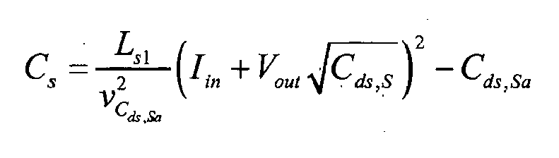
dans laquelle vCds,Sa est la tension aux bornes du condensateur drain - source Cds,Sa du dispositif de commutation auxiliaire Sa, la tension vCds,Sa étant dimensionnée sur la base de la tension nominale du dispositif de commutation. - Circuit d'amortissement actif selon l'une quelconque des revendications précédentes, dans lequel l'inductance du second inducteur (L s2) est donnée par la relation :

dans laquelle Vout est la tension de sortie et î Ls1 est le courant du premier inducteur L s1. - Circuit d'amortissement actif selon l'une quelconque des revendications précédentes, dans lequel la première direction va du premier point d'interface A au deuxième point d'interface B en passant par le troisième point d'interface C.
- Circuit d'amortissement actif selon l'une quelconque des revendications précédentes, dans lequel la première direction va du deuxième point d'interface B au premier point d'interface A en passant par le troisième point d'interface C.
- Convertisseur de courant comprenant le circuit d'amortissement actif selon l'une quelconque des revendications précédentes.
- Convertisseur de courant selon la revendication 9, dans lequel le convertisseur de courant comprend :un dispositif de diode principale connecté entre un premier noeud (A1') et un deuxième noeud (B') ;un dispositif de commutation principale connecté entre un premier noeud (A1') et un troisième noeud (C'), dans lequel :le premier point d'interface (A1) est connecté au premier noeud (A1') ;le deuxième point d'interface (B) est connecté au deuxième noeud (B') ; etle troisième point d'interface (C) est connecté au troisième noeud (C').
- Convertisseur de courant selon la revendication 9 ou la revendication 10, dans lequel le convertisseur de courant comprend :des diodes principales connectées entre une pluralité de premiers noeuds (A1' à Ax') et un deuxième noeud (B') ;des dispositifs de commutation principaux connectés entre les premiers noeuds (A1' à Ax') et un troisième noeud (C'), dans lequel :le circuit d'amortissement actif comprend des points d'interface (A1 à Ax), chaque premier point d'interface (A1 à Ax) étant connecté à l'un des premiers noeuds (A1' à Ax') ;le deuxième point d'interface (B) est connecté au deuxième noeud (B') ; etle troisième point d'interface (C) est connecté au troisième noeud (C').
Priority Applications (3)
| Application Number | Priority Date | Filing Date | Title |
|---|---|---|---|
| EP13161957.9A EP2787617B1 (fr) | 2013-04-02 | 2013-04-02 | Topologie d'amortissement actif |
| US14/242,288 US9331563B2 (en) | 2013-04-02 | 2014-04-01 | Active snubber topology |
| CN201410131020.2A CN104104224B (zh) | 2013-04-02 | 2014-04-02 | 有源缓冲器拓扑 |
Applications Claiming Priority (1)
| Application Number | Priority Date | Filing Date | Title |
|---|---|---|---|
| EP13161957.9A EP2787617B1 (fr) | 2013-04-02 | 2013-04-02 | Topologie d'amortissement actif |
Publications (2)
| Publication Number | Publication Date |
|---|---|
| EP2787617A1 EP2787617A1 (fr) | 2014-10-08 |
| EP2787617B1 true EP2787617B1 (fr) | 2015-11-04 |
Family
ID=48013855
Family Applications (1)
| Application Number | Title | Priority Date | Filing Date |
|---|---|---|---|
| EP13161957.9A Active EP2787617B1 (fr) | 2013-04-02 | 2013-04-02 | Topologie d'amortissement actif |
Country Status (3)
| Country | Link |
|---|---|
| US (1) | US9331563B2 (fr) |
| EP (1) | EP2787617B1 (fr) |
| CN (1) | CN104104224B (fr) |
Families Citing this family (16)
| Publication number | Priority date | Publication date | Assignee | Title |
|---|---|---|---|---|
| JP6461603B2 (ja) * | 2012-11-02 | 2019-01-30 | ローム株式会社 | チップコンデンサ、回路アセンブリ、および電子機器 |
| US20170005563A1 (en) * | 2014-01-07 | 2017-01-05 | Arizona Board Of Regents On Behalf Of Arizona State University | Zero-Voltage Transition in Power Converters with an Auxiliary Circuit |
| US9979283B2 (en) * | 2014-11-05 | 2018-05-22 | Samsung Sdi Co., Ltd. | DC boosting circuit with at least one energy storage element |
| DE102015122567A1 (de) * | 2015-12-22 | 2017-06-22 | NOVUM engineerING GmbH | Gleichstromwandler |
| US9941793B2 (en) | 2016-07-15 | 2018-04-10 | Dell Products, Lp | Snubber for voltage regulation |
| US10972014B2 (en) * | 2017-10-12 | 2021-04-06 | Rompower Technology Holdings, Llc | High efficiency passive clamp |
| US10505440B1 (en) * | 2018-08-31 | 2019-12-10 | Dialog Semiconductor (Uk) Limited | Active snubber for switching power converter |
| CN113841328B (zh) | 2019-05-21 | 2024-02-09 | 华为数字能源技术有限公司 | 升压转换器及控制方法 |
| US12184163B2 (en) * | 2019-05-28 | 2024-12-31 | Ngai Kit Franki Poon | Switching power supply apparatus |
| US10819244B1 (en) * | 2019-06-20 | 2020-10-27 | Abb Power Electronics Inc. | Single-stage isolated DC-DC converters with interleaved arms |
| CN112187032B (zh) | 2019-07-04 | 2022-03-15 | 台达电子工业股份有限公司 | 电源供应装置及其操作方法 |
| TWI701885B (zh) * | 2019-07-04 | 2020-08-11 | 台達電子工業股份有限公司 | 電源供應裝置及其操作方法 |
| IL271448A (en) * | 2019-12-15 | 2021-06-30 | Visic Tech Ltd | Overvoltage protection circuit |
| RU2725623C1 (ru) * | 2020-02-21 | 2020-07-03 | Акционерное общество "Чебоксарский электроаппаратный завод" | Устройство обнуления напряжения квазирезонансного типа |
| US11996785B1 (en) | 2022-11-17 | 2024-05-28 | Rompower Technology Holdings, Llc | High efficiency AC-DC converter |
| CN116995733B (zh) * | 2023-09-26 | 2023-12-22 | 安徽微伏特电源科技有限公司 | 一种反激式微型并网逆变器的多重缓冲系统及计算方法 |
Family Cites Families (15)
| Publication number | Priority date | Publication date | Assignee | Title |
|---|---|---|---|---|
| US4365171A (en) * | 1980-12-23 | 1982-12-21 | General Electric Company | Low loss snubber circuit |
| US4805079A (en) * | 1986-05-06 | 1989-02-14 | U.S. Philips Corp. | Switched voltage converter |
| JP2674341B2 (ja) * | 1991-03-27 | 1997-11-12 | 三菱電機株式会社 | 電力変換装置のスナバ回路 |
| US5418704A (en) | 1992-06-12 | 1995-05-23 | Center For Innovative Technology | Zero-voltage-transition pulse-width-modulated converters |
| US5313382A (en) | 1993-05-18 | 1994-05-17 | At&T Bell Laboratories | Reduced voltage/zero current transition boost power converter |
| TW291620B (fr) * | 1995-05-10 | 1996-11-21 | Philips Electronics Nv | |
| US5943200A (en) * | 1998-01-06 | 1999-08-24 | Lucent Technologies Inc. | Peak voltage clamping circuit for high frequency boost converter and method of operation thereof |
| US5959438A (en) | 1998-01-09 | 1999-09-28 | Delta Electronics, Inc. | Soft-switched boost converter with isolated active snubber |
| US6028418A (en) | 1999-02-11 | 2000-02-22 | Delta Electronics, Inc. | Boost converter with minimum-component-count active snubber |
| US6236191B1 (en) | 2000-06-02 | 2001-05-22 | Astec International Limited | Zero voltage switching boost topology |
| WO2002003533A1 (fr) * | 2000-07-05 | 2002-01-10 | Tdk Corporation | Systeme de conversion de courant electrique |
| US6348818B1 (en) * | 2000-08-14 | 2002-02-19 | Ledi-Lite Ltd. | Voltage-adder LED driver |
| TW497326B (en) | 2000-10-23 | 2002-08-01 | Delta Electronics Inc | Zero-voltage and zero-current boosting-type converter |
| KR100517195B1 (ko) | 2002-12-17 | 2005-09-27 | 한국항공우주연구원 | 소프트 스위칭 방식의 보조 스위치를 갖는 영전압 스위칭펄스폭 변조 방식의 직류-직류 전력변환기 |
| US6987675B2 (en) * | 2003-05-23 | 2006-01-17 | Delta Electronics, Inc. | Soft-switched power converters |
-
2013
- 2013-04-02 EP EP13161957.9A patent/EP2787617B1/fr active Active
-
2014
- 2014-04-01 US US14/242,288 patent/US9331563B2/en active Active
- 2014-04-02 CN CN201410131020.2A patent/CN104104224B/zh active Active
Also Published As
| Publication number | Publication date |
|---|---|
| US9331563B2 (en) | 2016-05-03 |
| EP2787617A1 (fr) | 2014-10-08 |
| CN104104224A (zh) | 2014-10-15 |
| US20140313627A1 (en) | 2014-10-23 |
| CN104104224B (zh) | 2016-09-28 |
Similar Documents
| Publication | Publication Date | Title |
|---|---|---|
| EP2787617B1 (fr) | Topologie d'amortissement actif | |
| Lee et al. | New zero-current-transition PWM DC/DC converters without current stress | |
| Smith et al. | Properties and synthesis of passive lossless soft-switching PWM converters | |
| US9318968B2 (en) | DC-DC converter circuit for high input-to-output voltage conversion | |
| US7110265B2 (en) | Non-isolated DC-DC converters with direct primary to load current | |
| US9985516B2 (en) | DC/DC converter and method for zero voltage switching | |
| Das et al. | A novel load adaptive ZVS auxiliary circuit for PWM three-level DC–DC converters | |
| WO2013037309A1 (fr) | Appareil de régulation adaptative de temps mort et procédé de commutation de convertisseurs de puissance | |
| JP6201586B2 (ja) | Dc/dcコンバータ | |
| Wang et al. | ZVS-PWM flyback converter with a simple auxiliary circuit | |
| Luo et al. | An active clamp high step-up boost converter with a coupled inductor | |
| Huang et al. | MHz GaN-based interleaved CRM bi-directional buck/boost converter with coupled inductor | |
| Xia et al. | High performance ZVT with bus clamping modulation technique for single phase full bridge inverters | |
| Pal et al. | A Zero-Current-Switched PWM Full Bridge DC-DC Converter | |
| Ai | A novel integrated nondissipative snubber for flyback converter | |
| Wu et al. | ZVS three‐phase current‐fed push–pull converter employing a simple active‐clamp circuit for voltage step‐up applications | |
| Balakrishnan et al. | Phase Shift Controlled Full Bridge DC-DC Converter with Less Circulating Loss | |
| Erickson et al. | Soft switching | |
| CN107294377A (zh) | 多谐振的dc‑dc变换器及直流电流源 | |
| KR101656021B1 (ko) | 직렬공진형 컨버터 | |
| KR101106505B1 (ko) | 소프트 스위칭 투-인덕터 부스트 컨버터 | |
| Mousavian et al. | A novel ZVT/ZCT PWM converter used for solar battery chargers with reduced conduction loss | |
| Peterson | Switch mode power supplies-a new approach for consumer audio systems | |
| RU2327274C1 (ru) | Полномостовой преобразователь постоянного напряжения с мягкой коммутацией | |
| Ahmed et al. | Extended soft-switching operation of the dual interleaved boost converter |
Legal Events
| Date | Code | Title | Description |
|---|---|---|---|
| PUAI | Public reference made under article 153(3) epc to a published international application that has entered the european phase |
Free format text: ORIGINAL CODE: 0009012 |
|
| 17P | Request for examination filed |
Effective date: 20130402 |
|
| AK | Designated contracting states |
Kind code of ref document: A1 Designated state(s): AL AT BE BG CH CY CZ DE DK EE ES FI FR GB GR HR HU IE IS IT LI LT LU LV MC MK MT NL NO PL PT RO RS SE SI SK SM TR |
|
| AX | Request for extension of the european patent |
Extension state: BA ME |
|
| GRAP | Despatch of communication of intention to grant a patent |
Free format text: ORIGINAL CODE: EPIDOSNIGR1 |
|
| R17P | Request for examination filed (corrected) |
Effective date: 20141204 |
|
| RBV | Designated contracting states (corrected) |
Designated state(s): AL AT BE BG CH CY CZ DE DK EE ES FI FR GB GR HR HU IE IS IT LI LT LU LV MC MK MT NL NO PL PT RO RS SE SI SK SM TR |
|
| INTG | Intention to grant announced |
Effective date: 20150113 |
|
| GRAS | Grant fee paid |
Free format text: ORIGINAL CODE: EPIDOSNIGR3 |
|
| GRAP | Despatch of communication of intention to grant a patent |
Free format text: ORIGINAL CODE: EPIDOSNIGR1 |
|
| INTG | Intention to grant announced |
Effective date: 20150713 |
|
| GRAA | (expected) grant |
Free format text: ORIGINAL CODE: 0009210 |
|
| AK | Designated contracting states |
Kind code of ref document: B1 Designated state(s): AL AT BE BG CH CY CZ DE DK EE ES FI FR GB GR HR HU IE IS IT LI LT LU LV MC MK MT NL NO PL PT RO RS SE SI SK SM TR |
|
| REG | Reference to a national code |
Ref country code: GB Ref legal event code: FG4D |
|
| REG | Reference to a national code |
Ref country code: CH Ref legal event code: EP |
|
| REG | Reference to a national code |
Ref country code: AT Ref legal event code: REF Ref document number: 759794 Country of ref document: AT Kind code of ref document: T Effective date: 20151115 |
|
| REG | Reference to a national code |
Ref country code: IE Ref legal event code: FG4D |
|
| REG | Reference to a national code |
Ref country code: DE Ref legal event code: R096 Ref document number: 602013003704 Country of ref document: DE |
|
| REG | Reference to a national code |
Ref country code: NL Ref legal event code: MP Effective date: 20151104 |
|
| REG | Reference to a national code |
Ref country code: LT Ref legal event code: MG4D |
|
| REG | Reference to a national code |
Ref country code: AT Ref legal event code: MK05 Ref document number: 759794 Country of ref document: AT Kind code of ref document: T Effective date: 20151104 |
|
| REG | Reference to a national code |
Ref country code: FR Ref legal event code: PLFP Year of fee payment: 4 |
|
| PG25 | Lapsed in a contracting state [announced via postgrant information from national office to epo] |
Ref country code: IS Free format text: LAPSE BECAUSE OF FAILURE TO SUBMIT A TRANSLATION OF THE DESCRIPTION OR TO PAY THE FEE WITHIN THE PRESCRIBED TIME-LIMIT Effective date: 20160304 Ref country code: NL Free format text: LAPSE BECAUSE OF FAILURE TO SUBMIT A TRANSLATION OF THE DESCRIPTION OR TO PAY THE FEE WITHIN THE PRESCRIBED TIME-LIMIT Effective date: 20151104 Ref country code: NO Free format text: LAPSE BECAUSE OF FAILURE TO SUBMIT A TRANSLATION OF THE DESCRIPTION OR TO PAY THE FEE WITHIN THE PRESCRIBED TIME-LIMIT Effective date: 20160204 Ref country code: ES Free format text: LAPSE BECAUSE OF FAILURE TO SUBMIT A TRANSLATION OF THE DESCRIPTION OR TO PAY THE FEE WITHIN THE PRESCRIBED TIME-LIMIT Effective date: 20151104 Ref country code: HR Free format text: LAPSE BECAUSE OF FAILURE TO SUBMIT A TRANSLATION OF THE DESCRIPTION OR TO PAY THE FEE WITHIN THE PRESCRIBED TIME-LIMIT Effective date: 20151104 Ref country code: LT Free format text: LAPSE BECAUSE OF FAILURE TO SUBMIT A TRANSLATION OF THE DESCRIPTION OR TO PAY THE FEE WITHIN THE PRESCRIBED TIME-LIMIT Effective date: 20151104 |
|
| PG25 | Lapsed in a contracting state [announced via postgrant information from national office to epo] |
Ref country code: PT Free format text: LAPSE BECAUSE OF FAILURE TO SUBMIT A TRANSLATION OF THE DESCRIPTION OR TO PAY THE FEE WITHIN THE PRESCRIBED TIME-LIMIT Effective date: 20160304 Ref country code: FI Free format text: LAPSE BECAUSE OF FAILURE TO SUBMIT A TRANSLATION OF THE DESCRIPTION OR TO PAY THE FEE WITHIN THE PRESCRIBED TIME-LIMIT Effective date: 20151104 Ref country code: GR Free format text: LAPSE BECAUSE OF FAILURE TO SUBMIT A TRANSLATION OF THE DESCRIPTION OR TO PAY THE FEE WITHIN THE PRESCRIBED TIME-LIMIT Effective date: 20160205 Ref country code: AT Free format text: LAPSE BECAUSE OF FAILURE TO SUBMIT A TRANSLATION OF THE DESCRIPTION OR TO PAY THE FEE WITHIN THE PRESCRIBED TIME-LIMIT Effective date: 20151104 Ref country code: RS Free format text: LAPSE BECAUSE OF FAILURE TO SUBMIT A TRANSLATION OF THE DESCRIPTION OR TO PAY THE FEE WITHIN THE PRESCRIBED TIME-LIMIT Effective date: 20151104 Ref country code: PL Free format text: LAPSE BECAUSE OF FAILURE TO SUBMIT A TRANSLATION OF THE DESCRIPTION OR TO PAY THE FEE WITHIN THE PRESCRIBED TIME-LIMIT Effective date: 20151104 Ref country code: SE Free format text: LAPSE BECAUSE OF FAILURE TO SUBMIT A TRANSLATION OF THE DESCRIPTION OR TO PAY THE FEE WITHIN THE PRESCRIBED TIME-LIMIT Effective date: 20151104 Ref country code: LV Free format text: LAPSE BECAUSE OF FAILURE TO SUBMIT A TRANSLATION OF THE DESCRIPTION OR TO PAY THE FEE WITHIN THE PRESCRIBED TIME-LIMIT Effective date: 20151104 |
|
| PG25 | Lapsed in a contracting state [announced via postgrant information from national office to epo] |
Ref country code: CZ Free format text: LAPSE BECAUSE OF FAILURE TO SUBMIT A TRANSLATION OF THE DESCRIPTION OR TO PAY THE FEE WITHIN THE PRESCRIBED TIME-LIMIT Effective date: 20151104 |
|
| REG | Reference to a national code |
Ref country code: DE Ref legal event code: R097 Ref document number: 602013003704 Country of ref document: DE |
|
| PG25 | Lapsed in a contracting state [announced via postgrant information from national office to epo] |
Ref country code: SK Free format text: LAPSE BECAUSE OF FAILURE TO SUBMIT A TRANSLATION OF THE DESCRIPTION OR TO PAY THE FEE WITHIN THE PRESCRIBED TIME-LIMIT Effective date: 20151104 Ref country code: BE Free format text: LAPSE BECAUSE OF NON-PAYMENT OF DUE FEES Effective date: 20160430 Ref country code: SM Free format text: LAPSE BECAUSE OF FAILURE TO SUBMIT A TRANSLATION OF THE DESCRIPTION OR TO PAY THE FEE WITHIN THE PRESCRIBED TIME-LIMIT Effective date: 20151104 Ref country code: DK Free format text: LAPSE BECAUSE OF FAILURE TO SUBMIT A TRANSLATION OF THE DESCRIPTION OR TO PAY THE FEE WITHIN THE PRESCRIBED TIME-LIMIT Effective date: 20151104 Ref country code: RO Free format text: LAPSE BECAUSE OF FAILURE TO SUBMIT A TRANSLATION OF THE DESCRIPTION OR TO PAY THE FEE WITHIN THE PRESCRIBED TIME-LIMIT Effective date: 20151104 Ref country code: EE Free format text: LAPSE BECAUSE OF FAILURE TO SUBMIT A TRANSLATION OF THE DESCRIPTION OR TO PAY THE FEE WITHIN THE PRESCRIBED TIME-LIMIT Effective date: 20151104 |
|
| PLBE | No opposition filed within time limit |
Free format text: ORIGINAL CODE: 0009261 |
|
| STAA | Information on the status of an ep patent application or granted ep patent |
Free format text: STATUS: NO OPPOSITION FILED WITHIN TIME LIMIT |
|
| 26N | No opposition filed |
Effective date: 20160805 |
|
| PG25 | Lapsed in a contracting state [announced via postgrant information from national office to epo] |
Ref country code: SI Free format text: LAPSE BECAUSE OF FAILURE TO SUBMIT A TRANSLATION OF THE DESCRIPTION OR TO PAY THE FEE WITHIN THE PRESCRIBED TIME-LIMIT Effective date: 20151104 |
|
| PG25 | Lapsed in a contracting state [announced via postgrant information from national office to epo] |
Ref country code: LU Free format text: LAPSE BECAUSE OF FAILURE TO SUBMIT A TRANSLATION OF THE DESCRIPTION OR TO PAY THE FEE WITHIN THE PRESCRIBED TIME-LIMIT Effective date: 20160402 Ref country code: BE Free format text: LAPSE BECAUSE OF FAILURE TO SUBMIT A TRANSLATION OF THE DESCRIPTION OR TO PAY THE FEE WITHIN THE PRESCRIBED TIME-LIMIT Effective date: 20151104 |
|
| REG | Reference to a national code |
Ref country code: IE Ref legal event code: MM4A |
|
| REG | Reference to a national code |
Ref country code: FR Ref legal event code: PLFP Year of fee payment: 5 |
|
| PG25 | Lapsed in a contracting state [announced via postgrant information from national office to epo] |
Ref country code: IE Free format text: LAPSE BECAUSE OF NON-PAYMENT OF DUE FEES Effective date: 20160402 |
|
| REG | Reference to a national code |
Ref country code: FR Ref legal event code: PLFP Year of fee payment: 6 |
|
| PG25 | Lapsed in a contracting state [announced via postgrant information from national office to epo] |
Ref country code: HU Free format text: LAPSE BECAUSE OF FAILURE TO SUBMIT A TRANSLATION OF THE DESCRIPTION OR TO PAY THE FEE WITHIN THE PRESCRIBED TIME-LIMIT; INVALID AB INITIO Effective date: 20130402 |
|
| PG25 | Lapsed in a contracting state [announced via postgrant information from national office to epo] |
Ref country code: MK Free format text: LAPSE BECAUSE OF FAILURE TO SUBMIT A TRANSLATION OF THE DESCRIPTION OR TO PAY THE FEE WITHIN THE PRESCRIBED TIME-LIMIT Effective date: 20151104 Ref country code: CY Free format text: LAPSE BECAUSE OF FAILURE TO SUBMIT A TRANSLATION OF THE DESCRIPTION OR TO PAY THE FEE WITHIN THE PRESCRIBED TIME-LIMIT Effective date: 20151104 Ref country code: MC Free format text: LAPSE BECAUSE OF FAILURE TO SUBMIT A TRANSLATION OF THE DESCRIPTION OR TO PAY THE FEE WITHIN THE PRESCRIBED TIME-LIMIT Effective date: 20151104 Ref country code: MT Free format text: LAPSE BECAUSE OF NON-PAYMENT OF DUE FEES Effective date: 20160430 |
|
| PG25 | Lapsed in a contracting state [announced via postgrant information from national office to epo] |
Ref country code: BG Free format text: LAPSE BECAUSE OF FAILURE TO SUBMIT A TRANSLATION OF THE DESCRIPTION OR TO PAY THE FEE WITHIN THE PRESCRIBED TIME-LIMIT Effective date: 20151104 |
|
| PG25 | Lapsed in a contracting state [announced via postgrant information from national office to epo] |
Ref country code: AL Free format text: LAPSE BECAUSE OF FAILURE TO SUBMIT A TRANSLATION OF THE DESCRIPTION OR TO PAY THE FEE WITHIN THE PRESCRIBED TIME-LIMIT Effective date: 20151104 Ref country code: TR Free format text: LAPSE BECAUSE OF FAILURE TO SUBMIT A TRANSLATION OF THE DESCRIPTION OR TO PAY THE FEE WITHIN THE PRESCRIBED TIME-LIMIT Effective date: 20151104 |
|
| REG | Reference to a national code |
Ref country code: CH Ref legal event code: PFUS Owner name: ABB SCHWEIZ AG, CH Free format text: FORMER OWNER: ABB RESEARCH LTD., CH |
|
| REG | Reference to a national code |
Ref country code: DE Ref legal event code: R081 Ref document number: 602013003704 Country of ref document: DE Owner name: ABB E-MOBILITY B.V., NL Free format text: FORMER OWNER: ABB RESEARCH LTD., ZUERICH, CH Ref country code: DE Ref legal event code: R081 Ref document number: 602013003704 Country of ref document: DE Owner name: ABB SCHWEIZ AG, CH Free format text: FORMER OWNER: ABB RESEARCH LTD., ZUERICH, CH |
|
| REG | Reference to a national code |
Ref country code: GB Ref legal event code: 732E Free format text: REGISTERED BETWEEN 20200206 AND 20200212 |
|
| REG | Reference to a national code |
Ref country code: DE Ref legal event code: R081 Ref document number: 602013003704 Country of ref document: DE Owner name: ABB E-MOBILITY B.V., NL Free format text: FORMER OWNER: ABB SCHWEIZ AG, BADEN, CH |
|
| REG | Reference to a national code |
Ref country code: GB Ref legal event code: 732E Free format text: REGISTERED BETWEEN 20230706 AND 20230712 |
|
| PGFP | Annual fee paid to national office [announced via postgrant information from national office to epo] |
Ref country code: DE Payment date: 20250422 Year of fee payment: 13 |
|
| PGFP | Annual fee paid to national office [announced via postgrant information from national office to epo] |
Ref country code: GB Payment date: 20250423 Year of fee payment: 13 |
|
| PGFP | Annual fee paid to national office [announced via postgrant information from national office to epo] |
Ref country code: IT Payment date: 20250424 Year of fee payment: 13 |
|
| PGFP | Annual fee paid to national office [announced via postgrant information from national office to epo] |
Ref country code: FR Payment date: 20250425 Year of fee payment: 13 |
|
| PGFP | Annual fee paid to national office [announced via postgrant information from national office to epo] |
Ref country code: CH Payment date: 20250501 Year of fee payment: 13 |