EP2787660B1 - Verfahren zur Verbesserung der Signalqualität eines durch eine nichtlineare Vorrichtung gesendeten digitalen Signals sowie Vorrichtung damit - Google Patents
Verfahren zur Verbesserung der Signalqualität eines durch eine nichtlineare Vorrichtung gesendeten digitalen Signals sowie Vorrichtung damit Download PDFInfo
- Publication number
- EP2787660B1 EP2787660B1 EP13162171.6A EP13162171A EP2787660B1 EP 2787660 B1 EP2787660 B1 EP 2787660B1 EP 13162171 A EP13162171 A EP 13162171A EP 2787660 B1 EP2787660 B1 EP 2787660B1
- Authority
- EP
- European Patent Office
- Prior art keywords
- level
- transition
- pulse
- digital signal
- overshoot
- Prior art date
- Legal status (The legal status is an assumption and is not a legal conclusion. Google has not performed a legal analysis and makes no representation as to the accuracy of the status listed.)
- Not-in-force
Links
- 238000000034 method Methods 0.000 title claims description 18
- 230000007704 transition Effects 0.000 claims description 179
- 230000005540 biological transmission Effects 0.000 claims description 8
- 238000004891 communication Methods 0.000 claims description 3
- 239000013307 optical fiber Substances 0.000 claims description 3
- 230000003287 optical effect Effects 0.000 description 55
- 230000010355 oscillation Effects 0.000 description 8
- 230000000694 effects Effects 0.000 description 3
- 238000007796 conventional method Methods 0.000 description 2
- 238000001914 filtration Methods 0.000 description 2
- 238000007493 shaping process Methods 0.000 description 2
- 230000006641 stabilisation Effects 0.000 description 2
- 238000011105 stabilization Methods 0.000 description 2
- RYGMFSIKBFXOCR-UHFFFAOYSA-N Copper Chemical compound [Cu] RYGMFSIKBFXOCR-UHFFFAOYSA-N 0.000 description 1
- 230000003213 activating effect Effects 0.000 description 1
- 230000015556 catabolic process Effects 0.000 description 1
- 238000006243 chemical reaction Methods 0.000 description 1
- 229910052802 copper Inorganic materials 0.000 description 1
- 239000010949 copper Substances 0.000 description 1
- 238000006731 degradation reaction Methods 0.000 description 1
- 230000001419 dependent effect Effects 0.000 description 1
- 230000001627 detrimental effect Effects 0.000 description 1
- 238000010586 diagram Methods 0.000 description 1
- 230000000704 physical effect Effects 0.000 description 1
- 230000008054 signal transmission Effects 0.000 description 1
- 238000011144 upstream manufacturing Methods 0.000 description 1
Images




Classifications
-
- H—ELECTRICITY
- H03—ELECTRONIC CIRCUITRY
- H03K—PULSE TECHNIQUE
- H03K5/00—Manipulating of pulses not covered by one of the other main groups of this subclass
- H03K5/01—Shaping pulses
-
- H—ELECTRICITY
- H04—ELECTRIC COMMUNICATION TECHNIQUE
- H04B—TRANSMISSION
- H04B10/00—Transmission systems employing electromagnetic waves other than radio-waves, e.g. infrared, visible or ultraviolet light, or employing corpuscular radiation, e.g. quantum communication
- H04B10/50—Transmitters
- H04B10/501—Structural aspects
- H04B10/502—LED transmitters
-
- H—ELECTRICITY
- H04—ELECTRIC COMMUNICATION TECHNIQUE
- H04B—TRANSMISSION
- H04B10/00—Transmission systems employing electromagnetic waves other than radio-waves, e.g. infrared, visible or ultraviolet light, or employing corpuscular radiation, e.g. quantum communication
- H04B10/50—Transmitters
- H04B10/58—Compensation for non-linear transmitter output
Definitions
- the present invention relates to a method for improving quality of a signal being transmitted at high speed through a non-linear electrical and / or optical device.
- the present invention also relates to an apparatus using this method.
- One cause of signal quality degradation is transmission of a signal through a bandwidth-limited channel, that is, one where the transmission is significantly lower above a certain frequency (the cutoff frequency). Passing a signal through such a channel results in attenuation of components at higher frequencies. This filtering of the transmitted signal affects the shape of the pulse that arrives at the receiver. Not only the shape of the pulse within its symbol period is changed, but it is also spread out over the subsequent symbol periods. When a signal is transmitted through such a channel, the spread pulse of each individual symbol will interfere with the following symbols.
- the bandwidth limitation can be due to the physical properties of the active components or a medium; for instance, at bit rates of 25 Gbps, a copper cable, being used in an electrical link, may have a cutoff frequency above which practically none of the transmitted signals will propagate. Therefore, in order to provide sufficient bandwidth for high speed data transmission applications (for instance, at bit rates of 25 Gbps), optical links are proposed. Transmission of data over an optical link, however, involves conversion of electrical digital signals into optical signals.
- a laser diode such as a Vertical Cavity Surface Emitting Laser (VCSEL)
- VCSEL Vertical Cavity Surface Emitting Laser
- the laser diode is a non-linear device, and therefore the laser diode affects the shape of its output pulse. Particularly, the pulse distortion can cause intersymbol interference.
- FIG 1 shows a schematic of a conventional transmitter for converting an electrical digital signal into an optical signal and outputting the optical signal to an optical fiber.
- the conventional transmitter 100 comprises a pre-emphasis driver 101 (that pre-distorts the signal) and a laser diode 102 connected to the pre-emphasis driver 101.
- the pre-emphasis driver 101 is adapted to receive at its input an electrical signal, to pre-emphasize the received signal, and to output pre-distorted electrical pulses.
- the laser diode 102 is adapted to receive at its input such electrical pulses from the pre-emphasis driver 101, to convert the received electrical pulses into optical signals, and to output the optical signals into the optical fiber (not shown in Fig. 1 ).
- the pulse shaping performed by the pre-emphasis driver 101 of the conventional transmitter 100 is explained by means of Figure 2 .
- the curve 201 represents the shape of a pulse of a digital (binary) signal input to the pre-emphasis driver 101. This pulse makes a first, positive transition from a lower level ("0"-level) to an upper level (“1 "-level), remains approximately constant at the upper level during the pulse lengths, and thereafter makes a second, negative transition from the upper level to the lower level.
- the curve 202 represents the shape of the signal output by the pre-emphasis circuit 101 when the square pulse 201 is applied to its input. This curve exhibits an overshoot immediately after the transition from "0"-level to "1"-level (the positive transition) and an undershoot immediately after the transition from "1"-level to "0"-level (the negative transition).
- the curve 202 makes a transition from "0"-level to "1"-level, overshoots the “1 “-level, relaxes to the "1 "-level, makes a transition from "1 "-level to "0”-level, undershoots the "0”-level, and then relaxes to the "0"-level.
- the pre-emphasis driver 101 of the conventional transmitter 100 is adapted to emphasize / peak an electrical digital signal during and / or immediately after the transition from one binary signal level to the other binary signal level.
- Figure 2 also shows the shape of the signal output by a bandwidth limited component being excited with a signal without such a pre-distortion and the shape of the signal output by the bandwidth limited component being excited with a signal having such a pre-distortion.
- Curve 212 exhibits more steep transitions between the lower and upper level compared to the curve 211.
- the pulse 222 exhibits shorter transition times (faster edges) compared to the pulse 221.
- pre-emphasis / peaking of the electrical pulse during and / or immediately after the transition from one binary signal level to the other binary signal level shortens the transition times at the edges of the pulse.
- the description of the behavior of the nonlinear component is detailed in Figure 3 .
- Figure 3 shows optical signals (in terms of optical power) output by the laser diode 102 when driven by the pre-emphasis driver 101.
- the curve 302 represents the shape of an optical pulse output by the laser diode 102, when an electrical pulse corresponding to curve 202 in Figure 2 , that is an electrical pulse showing pre-emphasis during / after the transition from one binary level to the other, is applied at the input of the laser diode 102.
- the curve 301 represents the shape of an optical pulse output by the laser diode 102, when an electrical pulse corresponding to curve 201 of Figure 2 , that is an electrical pulse without pre-emphasis, is applied at the input of the laser diode 102.
- the curve 301 exhibits an overshoot after the transition from "0"-level to "1 "-level and an undershoot after the transition from "0"-level to "1 "-level. This overshoot/undershoot is due to the self-resonance (relaxation oscillation) of the laser diode 102, and therefore is intrinsic to the optical pulse output by the laser diode 102.
- the curve 301 makes a transition from "0"-level to "1 "-level, overshoots the "1 "-level by the intrinsic overshoot, settles to the "1"-level, makes a transition from the "1"-level to the "0”-level, undershoots the "0"-level by the intrinsic undershoot, and then settles to the "0"-level.
- Curve 302 of Figure 3 also exhibits an overshoot after the transition from "0"-level to "1"-level and an undershoot after the transition from "1"-level to "0"-level.
- the overshoot of curve 302 exceeds the intrinsic overshoot of the laser diode 102 by the overshoot that is induced by the pre-emphasized electrical pulse applied at the input of the laser diode 102.
- the undershoot of curve 302 exceeds the intrinsic undershoot of the laser diode 102 by the undershoot that is induced by the pre-emphasized electrical pulse applied at the input of the laser diode 102.
- the curve 302 makes a transition from "0"-level to "1"-level, overshoots the "1 "-level by a resultant overshoot that is induced by both the intrinsic overshoot of the laser diode 102 and the overshoot of the pre-emphasized electrical input pulse, then relaxes to the "1"-level, makes a transition from "1"-level to "0"-level, undershoots the "0"-level by a resultant undershoot that is induced by both the intrinsic undershoot of the laser diode 102 and the undershoot of the pre-emphasized electrical input pulse, and then relaxes to "0"-level.
- the effect of the pre-emphasis driver 101 on the optical signal output by the laser diode 102 becomes evident when comparing the curves 302 and 301 of Figure 3 to each other. This comparison shows that the transition times from one optical power level to another optical power level are shorter for curve 302. In other words, pre-emphasizing/peaking the input pulse of the laser diode 102 during and / or immediately after the transition from one binary level to the other binary level steepens the edges of the optical signal output by the laser diode.
- the large overshoot of the optical pulse enhances the possibility of oscillations during the relaxation to the "1"-level.
- the large undershoot of the optical pulse enhances the possibility of oscillation during the relaxation to the "0"-level.
- These relaxation oscillations prolong the time required for the stabilization of the optical signal around an optical power level. If, however, the pulse duration is too short to ensure stabilization (setting) of the optical signal, intersymbol interference may occur. This is detrimental to signal integrity of the optical signal.
- Document US 2003/0212843 A1 discloses an apparatus for transmitting data from a source to a destination that is located a distance from the apparatus along a data bus.
- the apparatus comprising: a first driver for transmitting data along the data bus responsive to data being input thereto, the first driver producing data transitions between first and second driven logic states, the transitions having a first slope magnitude; a second driver connected in parallel with the first driver for selectively providing pre-emphasis to the data being transmitted by the first driver, whereby the slope of the transitions is increased at least during an initial portion of the transitions; and a data detector located upstream of the second driver for determining the transition history of data being input to the first driver and for activating the second driver as a function of the history.
- Document US 2008/0225106 A1 shows a circuit for driving a plurality of light emitting units.
- the circuit comprising: an overshoot-current generating unit that generates an overshoot current; and a current adding unit that biases a light emitting current that is determined based on an amount of light emitted from each of the light emitting units with the overshoot current, and supplies resultant current to each of the light emitting units.
- the present invention is based on the idea that pre-emphasizing a pulse of a digital (binary) signal before the transition / edge of the pulse effectively shortens the rise time and fall time of the pulse.
- the present invention also recognizes that the optical pulse output by a laser diode in response to an electric pulse having pre-emphasis before its transitions has shorter transition times than the optical pulse output by a laser diode in response to an electric pulse having pre-emphasis after its transitions. Also, the optical pulse output in response to a pulse having pre-emphasis before its transitions has a better signal quality than the optical pulse output in response to a pulse having pre-emphasis after / during its transitions.
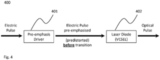
- the transmitter 400 comprises a pre-emphasis driver 401 and a non-linear device 402 connected to the pre-emphasis driver 401.
- the pre-emphasis driver 401 is adapted to receive at its input an electrical digital signal including at least one (binary) pulse, to pre-emphasize / peak the received electrical digital signal, and to output a pre-emphasized electrical digital signal.
- the non-linear device 402 is adapted to receive at its input the pre-emphasized electrical digital signal outputted by the pre-emphasis driver 401, to process the received signal, and to output a digital signal into a transmission medium (not shown in Fig.
- the non-linear device 402 is any one of a laser diode, a light-emitting diode, a transistor and an amplifier. Depending on the non-linear device 402 used, the digital signal output by the non-linear device 402 is either an electric signal or an optical signal.
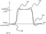
- the pulse 501 shown in Figure 5a is a particular case chosen for clarity. However, the present invention is not limited to this case, but is also applicable to the inverted pulse 511 shown in Fig. 5b .
- This pulse starts at an upper level ("0"-level), makes a first, negative transition from the upper level to a lower level ("-1 "-level), remains approximately constant at the lower level during the pulse length, and thereafter makes a second, positive transition from the lower level to the upper level.
- Curve 512 in Figure 5b represents the shape of the signal output by an pre-emphasis circuit according to the present invention in response to the pulse 511.
- This curve exhibits an overshoot immediately before (or next to) the negative transition from the upper level to the lower level and an undershoot immediately before (or next to) the positive transition from the lower level to the upper level.
- the curve 512 overshoots the upper level ("0"-level) by the overshoot 513, makes a first transition from the upper level to the lower level ("-1"-level), stays approximately constant at the lower level, undershoots the lower level ("-1"-level) by the undershoot 514, makes a second transition from the lower level to the upper level, and then stays approximately constant at the upper level.
- the pulse does not need to be part of a sequence of pulses.
- the present invention also applies to a single pulse signal, also called monopulse.
- the pre-emphasis driver 401 of the transmitter 400 is adapted to emphasis / peak a (binary) signal level of an electric digital signal immediately before the transition from one binary signal level to the other binary signal level.
- Table 1 Parameter Without pre-emphasis Pre-emphasis after the transition Pre-emphasis before the transition Overshoot [%] 6.0 16.9 6.4 Rise Time [ps] 14.7 13.4 12.8 Fall Time [ps] 15.7 14.3 13.3 Eye Opening Factor 0.84 0.64 0.59
- the effect of the pre-emphasis driver 401 becomes evident from Table 1.
- This table indicates: parameters of the pulse 203 output by a non-linear device in response to a square pulse 201 (without pre-emphasis), parameters of the pulse 202 output by the conventional pre-emphasize driver 101 (pre-emphasis after the transition) in response to the input pulse 201, and parameters of the pulse 502 output by the pre-emphasize driver 401 (pre-emphasis before the transition) in response to the input pulse 501.
- the eye opening factor relates to the eye diagram of the digital signal including the respective pulses and is equal to the ratio between inner eye opening (eye height) and eye amplitude.
- Table 1 shows that the output pulse 502 of the pre-emphasize driver 401 has the shortest rise time and the shortest fall time. This performance is achieved with an overshoot that is significantly lower than the overshoot induced by the conventional pre-emphasis driver. As the overshoot of the output pulse 502 of the pre-emphasize driver 401 is much lower than the overshoot of the output pulse 202 of the conventional pre-emphasize driver 101, the possibility of unwanted enhancement of relaxation oscillations is much lower in the output pulse 502 of the pre-emphasize driver 401 than in the output pulse 202 of the conventional pre-emphasize driver 201.
- Table 1 shows that the digital signal output by the pre-emphasize driver 401 and the digital signal output by the conventional pre-emphasize driver 201 have comparable eye opening factors, i.e., the short transition times of the output pulse of the pre-emphasis driver 401 are not achieved at the expense of less signal quality.
- Fig. 5a which shows the output signal of the pre-emphasis driver included in a transmitter according to a first preferred embodiment of the present invention
- the undershoot applied to the "0"-level is immediately before (or next to) the first (positive) transition of the pulse 502
- the overshoot applied to the "1 "-level is immediately before the second (negative) transition of the pulse 502.
- the present invention is not limited to this embodiment.
- the undershoot applied to the lower level is immediately before the first transition of pulse 502 and that the overshoot applied to the upper level is immediately before the second transition of pulse 502. It is rather sufficient that the undershoot applied to the lower level before the first transition of pulse 502 is closer to the first transition of the pulse 502 than to the second transition of a pulse preceding pulse 502, and/or that the overshoot applied to the upper level before the second transition of pulse 502 is closer to the second transition of pulse 502 than to the first transition of pulse 502.
- the overshoot applied to the upper level is immediately before the first transition of pulse 512 and that the undershoot applied to the lower level is immediately before the second transition of pulse 512. It is rather sufficient that the overshoot applied to the upper level before the first transition of pulse 512 is closer to the first transition of the pulse 512 than to the second transition of a pulse preceding pulse 512, and/or that the undershoot applied to the lower level before the second transition of pulse 512 is closer to the second transition of pulse 512 than to the first transition of pulse 512.
- Curve 521 of Figure 5c shows the shape of four pulses of a four-level digital signal input to the pre-emphasis driver included in a transmitter according to a third embodiment of the present invention.
- This signal makes a first transition from a first level ("0"-level) to a second level ("1"-level), which is higher than the first level, remains approximately constant at the second level for the duration of the pulse, thereafter makes a second transition from the second level to a third level ("2"-level), which is higher than the second level, remains approximately constant at the third level for the duration of the pulse, thereafter makes a third transition from the third level to a fourth level ("3"-level), which is higher than the third level, remains approximately constant at the fourth level for the duration of the pulse, thereafter makes a fourth transition from the fourth level to the third level, remains approximately constant at the third level for the duration of the pulse, and thereafter makes a fifth transition from the third level to the first level.
- the curve 522 represents the shape of the signal output by the pre-emphasis circuit included in the transmitter according to the third embodiment of the present invention in response to the fourth-level digital signal 521.
- This curve exhibits an undershoot immediately before (or next to) the positive transitions, i.e. the transitions from a lower level to a higher level, and an overshoot immediately before (or next to) the negative transitions. i.e. the transitions from a higher level to a lower level.
- the curve 522 undershoots the first level ("0"-level) by an undershoot 523-1, makes a first transition from the first level to the second level ("1 "-level), stays approximately constant at the second level, thereafter undershoots the second level by an undershoot 523-2, makes a second transition from the second level to the third level ("2"-level), stays approximately constant at the third level, thereafter undershoots the third level by an undershoot 523-3, makes a third transition from the third level to the fourth level ("3"-level), stays approximately constant at the fourth level, overshoots the fourth level by the overshoot 524-1, makes a fourth transition from the fourth level to the third level, stays approximately constant to the third level, and thereafter overshoots the third level by the overshoot 524-2, and makes a fifth transition from the third level to the first level.
- the four levels of the four-level digital signal shown in Fig. 5c have a positive polarity.
- the present invention is not limited to four-level digital signals whose levels are positive.
- the present invention is also applicable to four-level digital signals whose levels have a negative polarity.
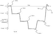
- curve 531 of Figure 5d shows the shape of four pulses of a four-level digital signal input to the pre-emphasis driver included in a transmitter according to a fourth embodiment of the present invention.
- This signal makes transitions between a first level ("0"-level), a second level ("-1 "-level), which is lower than the first level, a third level ("-2"-level), which is lower than the second level, and a fourth level ("-3"-level), which is lower than the third level.
- the first, second, third and fourth level have a negative polarity.
- the curve 532 represents the shape of the signal output by the pre-emphasis circuit included in the transmitter according to the fourth embodiment of the present invention in response to the fourth-level digital signal 531.
- This curve exhibits an undershoot 534-1 and 534-2 immediately before (or next to) the positive transitions, i.e. the transitions from a lower level to a higher level, and an overshoot 533-1, 533-2 and 533-3 immediately before (or next to) the negative transitions. i.e. the transitions from a higher level to a lower level.
- Figs. 5c and 5d the four levels of the four-level digital signal have the same polarity.
- the present invention is not limited to four-level digital signals whose levels have the same polarity.
- the present invention is also applicable to four-level digital signals whose levels have different polarities.
- the four-level digital signals shown in Figures 5c and 5d are only examples of multi-level digital signals to which the present invention applies and the scope of the present invention is not limited to them. Moreover, the present invention is applicable to any multi-level digital signal having an arbitrary number of levels, making transitions between any two levels of the digital signal, and making an arbitrary number of (positive and / or negative) transitions between two levels of the digital signal.
- a transmitter according to the present invention is adapted to process a digital signal having a plurality of levels m and which makes one or a plurality of transitions n between any two levels of the plurality of levels.
- m and n are natural numbers, m is greater or equal 2, and n is greater or equal 1.
- the transmitter according to the present invention includes a pre-emphasize driver which is adapted to emphasize / peak a level of the digital signal (immediately) before the transition from one, first level to another, second level of the plurality of levels.
- the pre-emphasize driver is adapted to pre-emphasize the digital signal by applying an undershoot to the first level (immediately) before the transition, when the first level is lower than the second level (i.e. at a positive transition), and to pre-emphasize the digital signal by applying an overshoot to the first level (immediately) before the first transition, when the first level is higher than the second level (i.e. at a negative transition).
- a fifth preferred embodiment of the present invention differs from the first preferred embodiment in that the non-linear device is a laser diode (for instance, a VCSEL).
- the fifth preferred embodiment converts electrical input pulses into optical output pulses.
- the laser diode can spread out the optical output pulse over the subsequent symbol period, which causes intersymbol distortion.
- the conventional method of pre-emphasizing the electrical input pulse shortens the rise time and fall time of the input pulse.
- the conventional method causes a high overshoot and undershoot in the optical output pulse (cf. Figure 3 ), which also can cause intersymbol interference.
- a method for pre-emphasizing the electrical input pulse that shortens the rise time and fall time of the optical output pulse, but does not significantly increase the overshoot and undershoot of the optical output pulse is preferable.
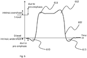
- Curve 602 in Figure 6 represents the optical power emitted by the laser diode in response to the electrical pulse 502 shown in Figure 5 .
- the curve 602 exhibits a first undershoot 610 before the transition from “0"-level to "1 "-level, a first overshoot 611 after the transition from “0"-level to "1”-level, a second overshoot 612 before the transition from “1"-level to "0”-level, and a second undershoot 613 after the transition from "1 "-level to "0”-level.
- the first undershoot 610 is due to the undershoot 503 of the input pulse 502.
- the first overshoot 611 is mainly due to the intrinsic overshoot (relaxation oscillations) of the laser diode.
- the second overshoot 612 is due to the overshoot 504 of the input pulse 502.
- the second undershoot 613 is mainly due to the intrinsic undershoot (relaxation oscillations) of the laser diode.
- the curve 602 undershoots the "0"-level by the first undershoot 610, makes a transition from “0"-level to “1 "-level, overshoots the "1 "-level by the first overshoot 611, relaxes to the "1 "-level, overshoots the "1 "-level again by the second overshoot 612, makes a transition from "1 "-level to "0”-level, undershoots the "0"-level by the second undershoot 613, and then relaxes to "0"-level.
- Table 2 indicates: parameters of the optical pulse output by the laser diode in response to the pulse 203 shown in Figure 2 (without pre-emphasis), parameters of the optical pulse output by the laser diode in response to the pulse 202 of Figure 2 (pre-emphasis during / after the transition), and parameters of the optical pulse output by the laser diode in response to the pulse 502 of Figure 5 (pre-emphasis before the transition).
- the following parameters are indicated: the overshoot of the optical signal beyond the "1 "-level; the rise time of the transition from "0"-level to "1 "-level; the fall time of the transition from "1 "-level to "0”-level; the eye opening factor; and the number of mask hits.
- Table 2 shows that the optical pulse output by the fifth preferred embodiment of the present invention has the shortest rise time and the shortest fall time. These transition times are achieved at an overshoot beyond the "1"-level which is much lower than the overshoot beyond the "1 "-level of the optical pulse output by the laser diode in response to pulse 202 of Fig. 2 (showing pre-emphasis after the transition). Having a smaller overshoot beyond the "1 "-level, the optical pulse output by the fifth preferred embodiment of the present invention is less susceptible to relaxation oscillations than the optical pulse output by the conventional transmitter shown in Figure 1 .
- Table 2 shows that the optical pulse output by the laser diode of the fifth preferred embodiment of the present invention achieves the highest eye opening factor and the lowest number of mask hits.
- the fifth preferred embodiment of the present invention not only shortens the rise time and the fall time of the optical output pulse 602 but also improves its signal quality.
- Conventional transmitter 101 Pre-emphasis driver of the conventional transmitter 102
- Laser diode of the conventional transmitter 201 Electrical pulse input to the conventional pre-emphasis driver 202
- Electrical pulse output by the conventional pre-emphasis driver 211 Electrical pulse output by a bandwidth limiting component excited with pulse 201 212
- Transmitter of the present invention 401 Pre-emphasis
- Optical pulse output by the laser diode of a transmitter of the present invention 610 First undershoot of the optical output pulse 611 First overshoot of the optical output pulse 612 Second overshoot of the optical output pulse 613 Second undershoot of the optical output pulse
Landscapes
- Physics & Mathematics (AREA)
- Nonlinear Science (AREA)
- Electromagnetism (AREA)
- Engineering & Computer Science (AREA)
- Computer Networks & Wireless Communication (AREA)
- Signal Processing (AREA)
- Dc Digital Transmission (AREA)
- Optical Communication System (AREA)
- Analogue/Digital Conversion (AREA)
- Picture Signal Circuits (AREA)
Claims (21)
- Verfahren zur Verarbeitung eines digitalen Signals durch eine nicht-lineare Einrichtung, wobei das digitale Signal einen ersten Übergang von einem ersten Pegel zu einem zweiten Pegel durchläuft, wobei das Verfahren umfasst:einen Schritt zur Voranhebung des digitalen Signals; undeinen Schritt zur Verarbeitung des vor-angehobenen digitalen Signals durch die nicht-lineare Einrichtung;dadurch gekennzeichnet, dass der Schritt der Voranhebung des digitalen Signals umfasst:Voranheben des digitalen Signals durch Anwendung einer Unterschwingung (503) auf den ersten Pegel vor dem ersten Übergang, wenn der erste Pegel niedriger als der zweite Pegel ist; und/oderVoranheben des digitalen Signals durch Anwendung einer Überschwingung (513) auf den ersten Pegel vor dem ersten Übergang, wenn der erste Pegel höher als der zweite Pegel ist.
- Verfahren nach Anspruch 1, wobei das digitale Signal ferner einen zweiten Übergang im Anschluss an den ersten Übergang von dem zweiten Pegel zu einem dritten Pegel durchläuft, und
der Schritt der Voranhebung des digitalen Signals ferner umfasst:Voranheben des digitalen Signals durch Anwendung einer Überschwingung (504, 534-2) auf den zweiten Pegel vor dem zweiten Übergang, wenn der zweite Pegel höher als der dritte Pegel ist; und/oderVoranheben des digitalen Signals durch Anwenden einer Unterschwingung (514, 523-2) auf den zweiten Pegel vor dem zweiten Übergang, wenn der zweite Pegel niedriger als der dritte Pegel ist. - Verfahren nach Anspruch 2, wobei der erste Pegel sich von dem dritten Pegel unterscheidet.
- Verfahren nach Anspruch 2, wobei der erste Pegel mit dem dritten Pegel übereinstimmt.
- Verfahren nach Anspruch 3 oder 4, wobei das digitale Signal ferner einen dritten Übergang vor dem ersten Übergang von einem vierten Pegel zu dem ersten Pegel durchläuft,
wenn der erste Pegel niedriger als der zweite Pegel ist, ist die auf den ersten Pegel vor dem ersten Übergang angewendete Unterschwingung näher an dem ersten Übergang als an dem dritten Übergang,
wenn der erste Pegel niedriger als der zweite Pegel ist, ist die vor dem zweiten Übergang auf den zweiten Pegel angewendete Überschwingung näher an dem zweiten Übergang als an dem ersten Übergang,
wenn der erste Pegel höher als der zweite Pegel ist, ist die vor dem ersten Übergang auf den ersten Pegel angewendete Überschwingung näher an dem ersten Übergang als an dem dritten Übergang, und
wenn der erste Pegel höher als der zweite Pegel ist, ist die vor dem zweiten Übergang auf den zweiten Pegel angewendete Unterschwingung näher an dem zweiten Übergang als an dem ersten Übergang. - Verfahren nach einem der Ansprüche 1 bis 5, wobei die auf den ersten Pegel angewendete Unterschwingung unmittelbar vor dem ersten Übergang liegt, oder
die auf den zweiten Pegel angewendete Unterschwingung unmittelbar vor dem zweiten Übergang liegt, oder
die auf den zweiten Pegel angewendete Überschwingung unmittelbar vor dem zweiten Übergang liegt, oder
die auf den ersten Pegel angewendete Überschwingung unmittelbar vor dem ersten Übergang liegt. - Verfahren nach einem der Ansprüche 1 bis 6, wobei der erste Pegel, der zweite Pegel und der dritte Pegel jeweils die gleiche Polarität haben.
- Verfahren nach einem der Ansprüche 1 bis 6, wobei ein Pegel aus dem ersten Pegel, dem zweiten Pegel und dem dritten Pegel eine erste Polarität hat und ein weiterer Pegel aus dem ersten Pegel, dem zweiten Pegel und dem dritten Pegel eine zweite Polarität hat, die sich von der ersten Polarität unterscheidet.
- Verfahren nach einem der Ansprüche 1 bis 8, wobei die nicht-lineare Einrichtung eine Laserdiode (402), eine lichtemittierende Diode, eine Fotodiode, ein Transistor oder ein Verstärker ist.
- Vorrichtung zur Verarbeitung eines digitalen Signals durch eine nicht-lineare Einrichtung, wobei das digitale Signal einen ersten Übergang von einem ersten Pegel zu einem zweiten Pegel durchläuft, wobei die Vorrichtung umfasst:einen Voranhebungs-Treiber (401) zur Voranhebung des digitalen Signals; undeine nicht-lineare Einrichtung (402) zur Verarbeitung des vor-angehobenen digitalen Signals, das von dem Voranhebungs-Treiber (401) ausgegeben wird;dadurch gekennzeichnet, dassder Voranhebungs-Treiber (401) ausgebildet ist, das digitale Signal voranzuheben durch Anwendung einer Unterschwingung (503) auf den ersten Pegel vor dem ersten Übergang, wenn der erste Pegel niedriger als der zweite Pegel ist; und/oderdas digitale Signal voranzuheben durch Anwendung einer Überschwingung (513) auf den ersten Pegel vor dem ersten Übergang, wenn der erste Pegel höher als der zweite Pegel ist.
- Vorrichtung nach Anspruch 10, wobei das digitale Signal ferner einen zweiten Übergang im Anschluss an den ersten Übergang von dem zweiten Pegel zu einem dritten Pegel durchläuft, und
der Voranhebungs-Treiber (401) ferner ausgebildet ist, das digitale Signal vor-anzuheben durch Anwendung einer Überschwingung (504, 534-2) auf den zweiten Pegel vor dem zweiten Übergang, wenn der zweite Pegel höher als der dritte Pegel ist; und/oder das digitale Signal vor-anzuheben durch Anwendung einer Unterschwingung (514, 523-2) auf den zweiten Pegel vor dem zweiten Übergang, wenn der zweite Pegel niedriger als der dritte Pegel ist. - Vorrichtung nach Anspruch 11, wobei sich der erste Pegel von dem zweiten Pegel unterscheidet.
- Vorrichtung nach Anspruch 11, wobei der erste Pegel mit dem dritten Pegel übereinstimmt.
- Vorrichtung nach Anspruch 12 oder 13, wobei das digitale Signal ferner vor dem ersten Übergang einen dritten Übergang von einem vierten Pegel zu dem ersten Pegel durchläuft,
wenn der erste Pegel niedriger als der zweite Pegel ist, ist die vor dem ersten Übergang auf den ersten Pegel angewendete Unterschwingung näher an dem ersten Übergang als an dem dritten Übergang,
wenn der erste Pegel niedriger als der zweite Pegel ist, ist die vor dem zweiten Übergang auf den zweiten Pegel angewendete Überschwingung näher an dem zweiten Übergang als an dem ersten Übergang,
wenn der erste Pegel höher als der zweite Pegel ist, ist die vor dem ersten Übergang auf den ersten Pegel angewendete Überschwingung näher an dem ersten Übergang als an dem dritten Übergang, und
wenn der erste Pegel höher als der zweite Pegel ist, ist die vor dem zweiten Übergang auf den zweiten Pegel angewendete Unterschwingung näher an dem zweiten Übergang als an dem ersten Übergang. - Vorrichtung nach einem der Ansprüche 10 bis 14, wobei die auf den ersten Pegel angewendete Unterschwingung unmittelbar vor dem ersten Übergang liegt, oder
die auf den zweiten Pegel angewendete Unterschwingung unmittelbar vor dem zweiten Übergang liegt, oder
die auf den zweiten Pegel angewendete Überschwingung unmittelbar vor dem zweiten Übergang liegt, oder
die auf den ersten Pegel angewendete Überschwingung unmittelbar vor dem ersten Übergang liegt. - Vorrichtung nach einem der Ansprüche 11 bis 15, wobei der erste Pegel, der zweite Pegel und der dritte Pegel jeweils die gleiche Polarität haben.
- Vorrichtung nach einem der Ansprüche 11 bis 15, wobei ein Pegel aus dem ersten Pegel, dem zweiten Pegel und dem dritten Pegel eine erste Polarität hat und ein weiterer Pegel aus dem ersten Pegel, dem zweiten Pegel und dem dritten Pegel eine zweite Polarität hat, die sich von der ersten Polarität unterscheidet.
- Vorrichtung nach einem der Ansprüche 10 bis 17, wobei die nicht-lineare Einrichtung eine Laserdiode (402), eine lichtemittierende Diode, eine Fotodiode, ein Transistor oder ein Verstärker ist.
- Sender (400) zum Senden eines digitalen Signals über ein Übertragungsmedium, wobei der Sender die Vorrichtung nach einem der Ansprüche 10 bis 18 aufweist.
- Sender nach Anspruch 19, wobei die nicht-lineare Einrichtung (402) eine Laserdiode und das Übertragungsmedium eine Lichtleitfaser ist.
- Kommunikationssystem, das den Sender nach Anspruch 19 oder 20 umfasst.
Priority Applications (8)
| Application Number | Priority Date | Filing Date | Title |
|---|---|---|---|
| EP13162171.6A EP2787660B1 (de) | 2013-04-03 | 2013-04-03 | Verfahren zur Verbesserung der Signalqualität eines durch eine nichtlineare Vorrichtung gesendeten digitalen Signals sowie Vorrichtung damit |
| SG10201401012WA SG10201401012WA (en) | 2013-04-03 | 2014-03-27 | Method for Improving Signal Quality of a digital Signal being Transmitted Through a Non-Linear Device and Apparatus using the Same |
| MYPI2014700796A MY167979A (en) | 2013-04-03 | 2014-04-02 | Method for improving signal quality of a digital signal being transmitted through a non-linear device and apparatus using the same |
| IL231875A IL231875A0 (en) | 2013-04-03 | 2014-04-02 | A method for improving the signal quality of a digital signal transmitted using a non-linear device and a system using it |
| JP2014076350A JP6486012B2 (ja) | 2013-04-03 | 2014-04-02 | 非線形デバイスに伝送されるデジタル信号の信号品質を改善する方法及びそれを使用する装置 |
| TW103112615A TW201445842A (zh) | 2013-04-03 | 2014-04-03 | 用於改良經由一非線性裝置傳輸之一數位信號之信號品質之方法及使用其之設備 |
| US14/244,783 US9178501B2 (en) | 2013-04-03 | 2014-04-03 | Method for improving signal quality of a digital signal being transmitted through a non-linear device and apparatus using the same |
| CN201410132306.2A CN104104449B (zh) | 2013-04-03 | 2014-04-03 | 通过非线性器件处理数字信号的方法和使用该方法的设备 |
Applications Claiming Priority (1)
| Application Number | Priority Date | Filing Date | Title |
|---|---|---|---|
| EP13162171.6A EP2787660B1 (de) | 2013-04-03 | 2013-04-03 | Verfahren zur Verbesserung der Signalqualität eines durch eine nichtlineare Vorrichtung gesendeten digitalen Signals sowie Vorrichtung damit |
Publications (2)
| Publication Number | Publication Date |
|---|---|
| EP2787660A1 EP2787660A1 (de) | 2014-10-08 |
| EP2787660B1 true EP2787660B1 (de) | 2017-09-27 |
Family
ID=48047880
Family Applications (1)
| Application Number | Title | Priority Date | Filing Date |
|---|---|---|---|
| EP13162171.6A Not-in-force EP2787660B1 (de) | 2013-04-03 | 2013-04-03 | Verfahren zur Verbesserung der Signalqualität eines durch eine nichtlineare Vorrichtung gesendeten digitalen Signals sowie Vorrichtung damit |
Country Status (8)
| Country | Link |
|---|---|
| US (1) | US9178501B2 (de) |
| EP (1) | EP2787660B1 (de) |
| JP (1) | JP6486012B2 (de) |
| CN (1) | CN104104449B (de) |
| IL (1) | IL231875A0 (de) |
| MY (1) | MY167979A (de) |
| SG (1) | SG10201401012WA (de) |
| TW (1) | TW201445842A (de) |
Families Citing this family (7)
| Publication number | Priority date | Publication date | Assignee | Title |
|---|---|---|---|---|
| JP6036210B2 (ja) * | 2012-11-19 | 2016-11-30 | 富士通株式会社 | エンファシス信号生成回路 |
| EP2999146B1 (de) * | 2014-09-16 | 2018-08-08 | Cosemi Technologies Inc. | Verfahren zur Verbesserung der Signalqualität eines in einer linearen Vorrichtung verarbeiteten digitalen Signals sowie Vorrichtung damit |
| CN107078809B (zh) * | 2014-10-29 | 2020-08-07 | 日本电信电话株式会社 | 突发光信号发送装置和突发光信号发送方法 |
| JP2016096221A (ja) * | 2014-11-13 | 2016-05-26 | 住友電気工業株式会社 | 駆動回路 |
| US20170104526A1 (en) * | 2015-10-07 | 2017-04-13 | Tyco Electronics Corporation | Stressed optical transmitter and method of compliance testing an optical receiver |
| WO2017216841A1 (ja) * | 2016-06-13 | 2017-12-21 | 株式会社日立製作所 | 光通信モジュール |
| CN113691393B (zh) * | 2021-07-14 | 2024-07-26 | 深圳市联洲国际技术有限公司 | 基于预加重的通信质量优化方法、装置、设备及存储介质 |
Family Cites Families (13)
| Publication number | Priority date | Publication date | Assignee | Title |
|---|---|---|---|---|
| DE3307309A1 (de) * | 1983-03-02 | 1984-09-13 | Bosch Gmbh Robert | Verfahren und anordnung zur optischen uebertragung eines elektrischen signals |
| US6480067B1 (en) * | 2000-11-27 | 2002-11-12 | Sirenza Microdevices, Inc. | Peaking control for wideband laser driver applications |
| US6373346B1 (en) * | 2000-11-27 | 2002-04-16 | Sirenza Microdevices, Inc. | Laser driver pre-emphasis and de-emphasis method and/or architecture with tuning and duty cycle control |
| US7051127B2 (en) * | 2002-05-10 | 2006-05-23 | Hewlett-Packard Development Company, L.P. | Method and apparatus for selectively providing data pre-emphasis based upon data content history |
| JP4340759B2 (ja) * | 2003-09-10 | 2009-10-07 | 独立行政法人産業技術総合研究所 | デジタルデータ伝送装置 |
| US7369591B1 (en) * | 2005-01-14 | 2008-05-06 | National Semiconductor Corporation | System for controlling peaking for a driver for a vertical-cavity surface-emitting laser |
| JP2007005484A (ja) * | 2005-06-22 | 2007-01-11 | Fujitsu Ltd | 光増幅装置及び光ファイバ |
| US8229303B1 (en) * | 2006-08-07 | 2012-07-24 | Clariphy Communications, Inc. | Reducing pulse narrowing in the transmitter signal that drives a limiting E/O converter for optical fiber channels |
| JP5083867B2 (ja) * | 2007-03-02 | 2012-11-28 | 株式会社リコー | 光源駆動装置、光走査装置及び画像形成装置 |
| US20130142520A1 (en) * | 2008-06-30 | 2013-06-06 | Chuan Xie | Anti-causal pre-emphasis for high speed optical transmission |
| US20110280265A1 (en) * | 2010-05-14 | 2011-11-17 | Institut National D'optique | Driver circuit for the direct modulation of a laser diode |
| JP5488330B2 (ja) * | 2010-08-18 | 2014-05-14 | 富士通株式会社 | 信号整形回路および光送信装置 |
| JP2012044396A (ja) * | 2010-08-18 | 2012-03-01 | Fujitsu Ltd | 駆動回路および光送信装置 |
-
2013
- 2013-04-03 EP EP13162171.6A patent/EP2787660B1/de not_active Not-in-force
-
2014
- 2014-03-27 SG SG10201401012WA patent/SG10201401012WA/en unknown
- 2014-04-02 IL IL231875A patent/IL231875A0/en unknown
- 2014-04-02 JP JP2014076350A patent/JP6486012B2/ja not_active Expired - Fee Related
- 2014-04-02 MY MYPI2014700796A patent/MY167979A/en unknown
- 2014-04-03 TW TW103112615A patent/TW201445842A/zh unknown
- 2014-04-03 CN CN201410132306.2A patent/CN104104449B/zh not_active Expired - Fee Related
- 2014-04-03 US US14/244,783 patent/US9178501B2/en not_active Expired - Fee Related
Non-Patent Citations (1)
| Title |
|---|
| None * |
Also Published As
| Publication number | Publication date |
|---|---|
| US9178501B2 (en) | 2015-11-03 |
| CN104104449A (zh) | 2014-10-15 |
| MY167979A (en) | 2018-10-09 |
| EP2787660A1 (de) | 2014-10-08 |
| IL231875A0 (en) | 2014-08-31 |
| CN104104449B (zh) | 2018-05-29 |
| JP2014204440A (ja) | 2014-10-27 |
| JP6486012B2 (ja) | 2019-03-20 |
| TW201445842A (zh) | 2014-12-01 |
| US20140301742A1 (en) | 2014-10-09 |
| SG10201401012WA (en) | 2014-11-27 |
Similar Documents
| Publication | Publication Date | Title |
|---|---|---|
| EP2787660A1 (de) | Verfahren zur Verbesserung der Signalqualität eines durch eine nichtlineare Vorrichtung gesendeten digitalen Signals sowie Vorrichtung damit | |
| US10598852B1 (en) | Digital-to-analog converter (DAC)-based driver for optical modulators | |
| US9735879B2 (en) | Near-threshold optical transmitter pre-distortion | |
| Zuo et al. | Single Lane 150-Gb/s, 100-Gb/s and 70-Gb/s 4-PAM Transmission over 100-m, 300-m and 500-m MMF Using 25-G Class 850nm VCSEL | |
| WO2002033921A1 (en) | Method and apparatus for optical transmission | |
| Castro et al. | Investigation of 60 Gb/s 4-PAM Using an 850 nm VCSEL and Multimode Fiber | |
| KR20100138982A (ko) | 자유-공간 광학 전송 시스템에서 디지털 데이터의 비-플러터 전송을 위한 방법 | |
| CN110089081A (zh) | 编码方法、解码方法、传输方法、解码设备、编码设备、传输设备 | |
| JP2010068029A (ja) | 光トランシーバ | |
| KR102064676B1 (ko) | 판정 궤환 등화기 회로 | |
| US20170187463A1 (en) | Delay-based nonlinear equalizer | |
| US7876852B2 (en) | Modulator device for generating an optical transfer signal modulated by binary signal | |
| WO2017216841A1 (ja) | 光通信モジュール | |
| Surampudi et al. | Raised cosine pulse shaping for pre-equalized optical wireless links | |
| US20050281563A1 (en) | Line driver with variable bandwidth control | |
| Hecht et al. | Up to 30-fold BER improvement using a data-dependent FFE switching technique for 112Gbit/s PAM-4 VCSEL based links | |
| Amari et al. | Probabilistic shaping for PAM-8 optical ethernet systems | |
| EP2999146B1 (de) | Verfahren zur Verbesserung der Signalqualität eines in einer linearen Vorrichtung verarbeiteten digitalen Signals sowie Vorrichtung damit | |
| US20170272164A1 (en) | Pulse amplitude modulation (pam) over multi-mode link with receiver spatial filtering | |
| CN103166701B (zh) | 在光传输中参数协商的方法、发送设备、接收设备及光模块 | |
| US20130177324A1 (en) | Sending/receiving system, sending/receiving method, and non-transitory computer-readable medium | |
| HK1236691A1 (en) | Method for improving signal quality of a digital signal being processed in a linear device and apparatus using the same | |
| CN117639953B (zh) | 一种非对称线性模拟均衡器、非对称线性模拟均衡技术的实现方法 | |
| US11658796B2 (en) | End-to-end link channel with lookup table(s) for equalization | |
| WO2003032491A1 (en) | Reduction of ringing and inter-symbol interference in optical communications |
Legal Events
| Date | Code | Title | Description |
|---|---|---|---|
| PUAI | Public reference made under article 153(3) epc to a published international application that has entered the european phase |
Free format text: ORIGINAL CODE: 0009012 |
|
| 17P | Request for examination filed |
Effective date: 20130925 |
|
| AK | Designated contracting states |
Kind code of ref document: A1 Designated state(s): AL AT BE BG CH CY CZ DE DK EE ES FI FR GB GR HR HU IE IS IT LI LT LU LV MC MK MT NL NO PL PT RO RS SE SI SK SM TR |
|
| AX | Request for extension of the european patent |
Extension state: BA ME |
|
| REG | Reference to a national code |
Ref country code: DE Ref legal event code: R079 Ref document number: 602013027044 Country of ref document: DE Free format text: PREVIOUS MAIN CLASS: H04B0010500000 Ipc: H03K0005010000 |
|
| RAP1 | Party data changed (applicant data changed or rights of an application transferred) |
Owner name: COSEMI TECHNOLOGIES, INC. |
|
| RIC1 | Information provided on ipc code assigned before grant |
Ipc: H03K 5/01 20060101AFI20170221BHEP Ipc: H04B 10/50 20130101ALI20170221BHEP Ipc: H04B 10/58 20130101ALI20170221BHEP |
|
| GRAP | Despatch of communication of intention to grant a patent |
Free format text: ORIGINAL CODE: EPIDOSNIGR1 |
|
| INTG | Intention to grant announced |
Effective date: 20170412 |
|
| RAP1 | Party data changed (applicant data changed or rights of an application transferred) |
Owner name: COSEMI TECHNOLOGIES INC. |
|
| GRAS | Grant fee paid |
Free format text: ORIGINAL CODE: EPIDOSNIGR3 |
|
| GRAA | (expected) grant |
Free format text: ORIGINAL CODE: 0009210 |
|
| AK | Designated contracting states |
Kind code of ref document: B1 Designated state(s): AL AT BE BG CH CY CZ DE DK EE ES FI FR GB GR HR HU IE IS IT LI LT LU LV MC MK MT NL NO PL PT RO RS SE SI SK SM TR |
|
| REG | Reference to a national code |
Ref country code: GB Ref legal event code: FG4D |
|
| REG | Reference to a national code |
Ref country code: CH Ref legal event code: EP |
|
| REG | Reference to a national code |
Ref country code: AT Ref legal event code: REF Ref document number: 932873 Country of ref document: AT Kind code of ref document: T Effective date: 20171015 |
|
| REG | Reference to a national code |
Ref country code: IE Ref legal event code: FG4D |
|
| REG | Reference to a national code |
Ref country code: DE Ref legal event code: R096 Ref document number: 602013027044 Country of ref document: DE |
|
| PG25 | Lapsed in a contracting state [announced via postgrant information from national office to epo] |
Ref country code: FI Free format text: LAPSE BECAUSE OF FAILURE TO SUBMIT A TRANSLATION OF THE DESCRIPTION OR TO PAY THE FEE WITHIN THE PRESCRIBED TIME-LIMIT Effective date: 20170927 Ref country code: LT Free format text: LAPSE BECAUSE OF FAILURE TO SUBMIT A TRANSLATION OF THE DESCRIPTION OR TO PAY THE FEE WITHIN THE PRESCRIBED TIME-LIMIT Effective date: 20170927 Ref country code: NO Free format text: LAPSE BECAUSE OF FAILURE TO SUBMIT A TRANSLATION OF THE DESCRIPTION OR TO PAY THE FEE WITHIN THE PRESCRIBED TIME-LIMIT Effective date: 20171227 Ref country code: SE Free format text: LAPSE BECAUSE OF FAILURE TO SUBMIT A TRANSLATION OF THE DESCRIPTION OR TO PAY THE FEE WITHIN THE PRESCRIBED TIME-LIMIT Effective date: 20170927 Ref country code: HR Free format text: LAPSE BECAUSE OF FAILURE TO SUBMIT A TRANSLATION OF THE DESCRIPTION OR TO PAY THE FEE WITHIN THE PRESCRIBED TIME-LIMIT Effective date: 20170927 |
|
| REG | Reference to a national code |
Ref country code: NL Ref legal event code: MP Effective date: 20170927 |
|
| REG | Reference to a national code |
Ref country code: LT Ref legal event code: MG4D |
|
| REG | Reference to a national code |
Ref country code: AT Ref legal event code: MK05 Ref document number: 932873 Country of ref document: AT Kind code of ref document: T Effective date: 20170927 |
|
| PG25 | Lapsed in a contracting state [announced via postgrant information from national office to epo] |
Ref country code: RS Free format text: LAPSE BECAUSE OF FAILURE TO SUBMIT A TRANSLATION OF THE DESCRIPTION OR TO PAY THE FEE WITHIN THE PRESCRIBED TIME-LIMIT Effective date: 20170927 Ref country code: LV Free format text: LAPSE BECAUSE OF FAILURE TO SUBMIT A TRANSLATION OF THE DESCRIPTION OR TO PAY THE FEE WITHIN THE PRESCRIBED TIME-LIMIT Effective date: 20170927 Ref country code: BG Free format text: LAPSE BECAUSE OF FAILURE TO SUBMIT A TRANSLATION OF THE DESCRIPTION OR TO PAY THE FEE WITHIN THE PRESCRIBED TIME-LIMIT Effective date: 20171227 Ref country code: GR Free format text: LAPSE BECAUSE OF FAILURE TO SUBMIT A TRANSLATION OF THE DESCRIPTION OR TO PAY THE FEE WITHIN THE PRESCRIBED TIME-LIMIT Effective date: 20171228 |
|
| PG25 | Lapsed in a contracting state [announced via postgrant information from national office to epo] |
Ref country code: NL Free format text: LAPSE BECAUSE OF FAILURE TO SUBMIT A TRANSLATION OF THE DESCRIPTION OR TO PAY THE FEE WITHIN THE PRESCRIBED TIME-LIMIT Effective date: 20170927 |
|
| REG | Reference to a national code |
Ref country code: FR Ref legal event code: PLFP Year of fee payment: 6 |
|
| PG25 | Lapsed in a contracting state [announced via postgrant information from national office to epo] |
Ref country code: ES Free format text: LAPSE BECAUSE OF FAILURE TO SUBMIT A TRANSLATION OF THE DESCRIPTION OR TO PAY THE FEE WITHIN THE PRESCRIBED TIME-LIMIT Effective date: 20170927 Ref country code: RO Free format text: LAPSE BECAUSE OF FAILURE TO SUBMIT A TRANSLATION OF THE DESCRIPTION OR TO PAY THE FEE WITHIN THE PRESCRIBED TIME-LIMIT Effective date: 20170927 Ref country code: CZ Free format text: LAPSE BECAUSE OF FAILURE TO SUBMIT A TRANSLATION OF THE DESCRIPTION OR TO PAY THE FEE WITHIN THE PRESCRIBED TIME-LIMIT Effective date: 20170927 |
|
| PG25 | Lapsed in a contracting state [announced via postgrant information from national office to epo] |
Ref country code: EE Free format text: LAPSE BECAUSE OF FAILURE TO SUBMIT A TRANSLATION OF THE DESCRIPTION OR TO PAY THE FEE WITHIN THE PRESCRIBED TIME-LIMIT Effective date: 20170927 Ref country code: AT Free format text: LAPSE BECAUSE OF FAILURE TO SUBMIT A TRANSLATION OF THE DESCRIPTION OR TO PAY THE FEE WITHIN THE PRESCRIBED TIME-LIMIT Effective date: 20170927 Ref country code: IT Free format text: LAPSE BECAUSE OF FAILURE TO SUBMIT A TRANSLATION OF THE DESCRIPTION OR TO PAY THE FEE WITHIN THE PRESCRIBED TIME-LIMIT Effective date: 20170927 Ref country code: IS Free format text: LAPSE BECAUSE OF FAILURE TO SUBMIT A TRANSLATION OF THE DESCRIPTION OR TO PAY THE FEE WITHIN THE PRESCRIBED TIME-LIMIT Effective date: 20180127 Ref country code: SK Free format text: LAPSE BECAUSE OF FAILURE TO SUBMIT A TRANSLATION OF THE DESCRIPTION OR TO PAY THE FEE WITHIN THE PRESCRIBED TIME-LIMIT Effective date: 20170927 Ref country code: SM Free format text: LAPSE BECAUSE OF FAILURE TO SUBMIT A TRANSLATION OF THE DESCRIPTION OR TO PAY THE FEE WITHIN THE PRESCRIBED TIME-LIMIT Effective date: 20170927 |
|
| REG | Reference to a national code |
Ref country code: DE Ref legal event code: R097 Ref document number: 602013027044 Country of ref document: DE |
|
| PG25 | Lapsed in a contracting state [announced via postgrant information from national office to epo] |
Ref country code: DK Free format text: LAPSE BECAUSE OF FAILURE TO SUBMIT A TRANSLATION OF THE DESCRIPTION OR TO PAY THE FEE WITHIN THE PRESCRIBED TIME-LIMIT Effective date: 20170927 |
|
| PLBE | No opposition filed within time limit |
Free format text: ORIGINAL CODE: 0009261 |
|
| STAA | Information on the status of an ep patent application or granted ep patent |
Free format text: STATUS: NO OPPOSITION FILED WITHIN TIME LIMIT |
|
| PG25 | Lapsed in a contracting state [announced via postgrant information from national office to epo] |
Ref country code: PL Free format text: LAPSE BECAUSE OF FAILURE TO SUBMIT A TRANSLATION OF THE DESCRIPTION OR TO PAY THE FEE WITHIN THE PRESCRIBED TIME-LIMIT Effective date: 20170927 |
|
| 26N | No opposition filed |
Effective date: 20180628 |
|
| PG25 | Lapsed in a contracting state [announced via postgrant information from national office to epo] |
Ref country code: SI Free format text: LAPSE BECAUSE OF FAILURE TO SUBMIT A TRANSLATION OF THE DESCRIPTION OR TO PAY THE FEE WITHIN THE PRESCRIBED TIME-LIMIT Effective date: 20170927 Ref country code: MC Free format text: LAPSE BECAUSE OF FAILURE TO SUBMIT A TRANSLATION OF THE DESCRIPTION OR TO PAY THE FEE WITHIN THE PRESCRIBED TIME-LIMIT Effective date: 20170927 |
|
| REG | Reference to a national code |
Ref country code: CH Ref legal event code: PL |
|
| REG | Reference to a national code |
Ref country code: IE Ref legal event code: MM4A |
|
| PG25 | Lapsed in a contracting state [announced via postgrant information from national office to epo] |
Ref country code: LU Free format text: LAPSE BECAUSE OF NON-PAYMENT OF DUE FEES Effective date: 20180403 |
|
| PG25 | Lapsed in a contracting state [announced via postgrant information from national office to epo] |
Ref country code: LI Free format text: LAPSE BECAUSE OF NON-PAYMENT OF DUE FEES Effective date: 20180430 Ref country code: CH Free format text: LAPSE BECAUSE OF NON-PAYMENT OF DUE FEES Effective date: 20180430 |
|
| PG25 | Lapsed in a contracting state [announced via postgrant information from national office to epo] |
Ref country code: IE Free format text: LAPSE BECAUSE OF NON-PAYMENT OF DUE FEES Effective date: 20180403 |
|
| PG25 | Lapsed in a contracting state [announced via postgrant information from national office to epo] |
Ref country code: MT Free format text: LAPSE BECAUSE OF NON-PAYMENT OF DUE FEES Effective date: 20180403 |
|
| PG25 | Lapsed in a contracting state [announced via postgrant information from national office to epo] |
Ref country code: TR Free format text: LAPSE BECAUSE OF FAILURE TO SUBMIT A TRANSLATION OF THE DESCRIPTION OR TO PAY THE FEE WITHIN THE PRESCRIBED TIME-LIMIT Effective date: 20170927 |
|
| PG25 | Lapsed in a contracting state [announced via postgrant information from national office to epo] |
Ref country code: PT Free format text: LAPSE BECAUSE OF FAILURE TO SUBMIT A TRANSLATION OF THE DESCRIPTION OR TO PAY THE FEE WITHIN THE PRESCRIBED TIME-LIMIT Effective date: 20170927 Ref country code: HU Free format text: LAPSE BECAUSE OF FAILURE TO SUBMIT A TRANSLATION OF THE DESCRIPTION OR TO PAY THE FEE WITHIN THE PRESCRIBED TIME-LIMIT; INVALID AB INITIO Effective date: 20130403 |
|
| PG25 | Lapsed in a contracting state [announced via postgrant information from national office to epo] |
Ref country code: CY Free format text: LAPSE BECAUSE OF FAILURE TO SUBMIT A TRANSLATION OF THE DESCRIPTION OR TO PAY THE FEE WITHIN THE PRESCRIBED TIME-LIMIT Effective date: 20170927 Ref country code: MK Free format text: LAPSE BECAUSE OF NON-PAYMENT OF DUE FEES Effective date: 20170927 |
|
| PG25 | Lapsed in a contracting state [announced via postgrant information from national office to epo] |
Ref country code: AL Free format text: LAPSE BECAUSE OF FAILURE TO SUBMIT A TRANSLATION OF THE DESCRIPTION OR TO PAY THE FEE WITHIN THE PRESCRIBED TIME-LIMIT Effective date: 20170927 |
|
| REG | Reference to a national code |
Ref country code: DE Ref legal event code: R081 Ref document number: 602013027044 Country of ref document: DE Owner name: MOBIX LABS, INC. (N.D.GES.D. STAATES DELAWARE), US Free format text: FORMER OWNER: COSEMI TECHNOLOGIES INC., IRVINE, CALIF., US |
|
| REG | Reference to a national code |
Ref country code: GB Ref legal event code: 732E Free format text: REGISTERED BETWEEN 20220421 AND 20220427 |
|
| REG | Reference to a national code |
Ref country code: BE Ref legal event code: PD Owner name: MOBIX LABS, INC.; US Free format text: DETAILS ASSIGNMENT: CHANGE OF OWNER(S), ASSIGNMENT; FORMER OWNER NAME: COSEMI TECHNOLOGIES INC. Effective date: 20220412 |
|
| PGFP | Annual fee paid to national office [announced via postgrant information from national office to epo] |
Ref country code: GB Payment date: 20220425 Year of fee payment: 10 Ref country code: FR Payment date: 20220425 Year of fee payment: 10 Ref country code: DE Payment date: 20220429 Year of fee payment: 10 |
|
| PGFP | Annual fee paid to national office [announced via postgrant information from national office to epo] |
Ref country code: BE Payment date: 20220422 Year of fee payment: 10 |
|
| REG | Reference to a national code |
Ref country code: DE Ref legal event code: R119 Ref document number: 602013027044 Country of ref document: DE |
|
| GBPC | Gb: european patent ceased through non-payment of renewal fee |
Effective date: 20230403 |
|
| REG | Reference to a national code |
Ref country code: BE Ref legal event code: MM Effective date: 20230430 |
|
| PG25 | Lapsed in a contracting state [announced via postgrant information from national office to epo] |
Ref country code: GB Free format text: LAPSE BECAUSE OF NON-PAYMENT OF DUE FEES Effective date: 20230403 |
|
| PG25 | Lapsed in a contracting state [announced via postgrant information from national office to epo] |
Ref country code: GB Free format text: LAPSE BECAUSE OF NON-PAYMENT OF DUE FEES Effective date: 20230403 Ref country code: FR Free format text: LAPSE BECAUSE OF NON-PAYMENT OF DUE FEES Effective date: 20230430 Ref country code: DE Free format text: LAPSE BECAUSE OF NON-PAYMENT OF DUE FEES Effective date: 20231103 |
|
| PG25 | Lapsed in a contracting state [announced via postgrant information from national office to epo] |
Ref country code: BE Free format text: LAPSE BECAUSE OF NON-PAYMENT OF DUE FEES Effective date: 20230430 |