EP2792166B1 - Dispositif électronique portable à porter à l'oreille et procédé de fonctionnement d'un dispositif électronique portable - Google Patents
Dispositif électronique portable à porter à l'oreille et procédé de fonctionnement d'un dispositif électronique portable Download PDFInfo
- Publication number
- EP2792166B1 EP2792166B1 EP11799283.4A EP11799283A EP2792166B1 EP 2792166 B1 EP2792166 B1 EP 2792166B1 EP 11799283 A EP11799283 A EP 11799283A EP 2792166 B1 EP2792166 B1 EP 2792166B1
- Authority
- EP
- European Patent Office
- Prior art keywords
- voltage
- boost converter
- portable electronic
- electronic device
- duty cycle
- Prior art date
- Legal status (The legal status is an assumption and is not a legal conclusion. Google has not performed a legal analysis and makes no representation as to the accuracy of the status listed.)
- Active
Links
Images


Classifications
-
- H—ELECTRICITY
- H04—ELECTRIC COMMUNICATION TECHNIQUE
- H04R—LOUDSPEAKERS, MICROPHONES, GRAMOPHONE PICK-UPS OR LIKE ACOUSTIC ELECTROMECHANICAL TRANSDUCERS; ELECTRIC HEARING AIDS; PUBLIC ADDRESS SYSTEMS
- H04R25/00—Electric hearing aids
-
- H—ELECTRICITY
- H04—ELECTRIC COMMUNICATION TECHNIQUE
- H04R—LOUDSPEAKERS, MICROPHONES, GRAMOPHONE PICK-UPS OR LIKE ACOUSTIC ELECTROMECHANICAL TRANSDUCERS; ELECTRIC HEARING AIDS; PUBLIC ADDRESS SYSTEMS
- H04R1/00—Details of transducers, loudspeakers or microphones
- H04R1/10—Earpieces; Attachments therefor ; Earphones; Monophonic headphones
- H04R1/1025—Accumulators specially adapted for earpieces; Arrangements specially adapted for charging thereof
-
- H—ELECTRICITY
- H04—ELECTRIC COMMUNICATION TECHNIQUE
- H04R—LOUDSPEAKERS, MICROPHONES, GRAMOPHONE PICK-UPS OR LIKE ACOUSTIC ELECTROMECHANICAL TRANSDUCERS; ELECTRIC HEARING AIDS; PUBLIC ADDRESS SYSTEMS
- H04R25/00—Electric hearing aids
- H04R25/02—Electric hearing aids adapted to be supported entirely by ear
-
- H—ELECTRICITY
- H01—ELECTRIC ELEMENTS
- H01M—PROCESSES OR MEANS, e.g. BATTERIES, FOR THE DIRECT CONVERSION OF CHEMICAL ENERGY INTO ELECTRICAL ENERGY
- H01M2250/00—Fuel cells for particular applications; Specific features of fuel cell system
- H01M2250/30—Fuel cells in portable systems, e.g. mobile phone, laptop
-
- H—ELECTRICITY
- H01—ELECTRIC ELEMENTS
- H01M—PROCESSES OR MEANS, e.g. BATTERIES, FOR THE DIRECT CONVERSION OF CHEMICAL ENERGY INTO ELECTRICAL ENERGY
- H01M8/00—Fuel cells; Manufacture thereof
- H01M8/10—Fuel cells with solid electrolytes
- H01M8/1009—Fuel cells with solid electrolytes with one of the reactants being liquid, solid or liquid-charged
- H01M8/1011—Direct alcohol fuel cells [DAFC], e.g. direct methanol fuel cells [DMFC]
-
- H—ELECTRICITY
- H01—ELECTRIC ELEMENTS
- H01M—PROCESSES OR MEANS, e.g. BATTERIES, FOR THE DIRECT CONVERSION OF CHEMICAL ENERGY INTO ELECTRICAL ENERGY
- H01M8/00—Fuel cells; Manufacture thereof
- H01M8/10—Fuel cells with solid electrolytes
- H01M8/1009—Fuel cells with solid electrolytes with one of the reactants being liquid, solid or liquid-charged
- H01M8/1011—Direct alcohol fuel cells [DAFC], e.g. direct methanol fuel cells [DMFC]
- H01M8/1013—Other direct alcohol fuel cells [DAFC]
-
- H—ELECTRICITY
- H04—ELECTRIC COMMUNICATION TECHNIQUE
- H04R—LOUDSPEAKERS, MICROPHONES, GRAMOPHONE PICK-UPS OR LIKE ACOUSTIC ELECTROMECHANICAL TRANSDUCERS; ELECTRIC HEARING AIDS; PUBLIC ADDRESS SYSTEMS
- H04R2225/00—Details of deaf aids covered by H04R25/00, not provided for in any of its subgroups
- H04R2225/31—Aspects of the use of accumulators in hearing aids, e.g. rechargeable batteries or fuel cells
-
- H—ELECTRICITY
- H04—ELECTRIC COMMUNICATION TECHNIQUE
- H04R—LOUDSPEAKERS, MICROPHONES, GRAMOPHONE PICK-UPS OR LIKE ACOUSTIC ELECTROMECHANICAL TRANSDUCERS; ELECTRIC HEARING AIDS; PUBLIC ADDRESS SYSTEMS
- H04R2225/00—Details of deaf aids covered by H04R25/00, not provided for in any of its subgroups
- H04R2225/33—Aspects relating to adaptation of the battery voltage, e.g. its regulation, increase or decrease
-
- H—ELECTRICITY
- H04—ELECTRIC COMMUNICATION TECHNIQUE
- H04R—LOUDSPEAKERS, MICROPHONES, GRAMOPHONE PICK-UPS OR LIKE ACOUSTIC ELECTROMECHANICAL TRANSDUCERS; ELECTRIC HEARING AIDS; PUBLIC ADDRESS SYSTEMS
- H04R2225/00—Details of deaf aids covered by H04R25/00, not provided for in any of its subgroups
- H04R2225/67—Implantable hearing aids or parts thereof not covered by H04R25/606
-
- H—ELECTRICITY
- H04—ELECTRIC COMMUNICATION TECHNIQUE
- H04R—LOUDSPEAKERS, MICROPHONES, GRAMOPHONE PICK-UPS OR LIKE ACOUSTIC ELECTROMECHANICAL TRANSDUCERS; ELECTRIC HEARING AIDS; PUBLIC ADDRESS SYSTEMS
- H04R2460/00—Details of hearing devices, i.e. of ear- or headphones covered by H04R1/10 or H04R5/033 but not provided for in any of their subgroups, or of hearing aids covered by H04R25/00 but not provided for in any of its subgroups
- H04R2460/03—Aspects of the reduction of energy consumption in hearing devices
-
- Y—GENERAL TAGGING OF NEW TECHNOLOGICAL DEVELOPMENTS; GENERAL TAGGING OF CROSS-SECTIONAL TECHNOLOGIES SPANNING OVER SEVERAL SECTIONS OF THE IPC; TECHNICAL SUBJECTS COVERED BY FORMER USPC CROSS-REFERENCE ART COLLECTIONS [XRACs] AND DIGESTS
- Y02—TECHNOLOGIES OR APPLICATIONS FOR MITIGATION OR ADAPTATION AGAINST CLIMATE CHANGE
- Y02B—CLIMATE CHANGE MITIGATION TECHNOLOGIES RELATED TO BUILDINGS, e.g. HOUSING, HOUSE APPLIANCES OR RELATED END-USER APPLICATIONS
- Y02B90/00—Enabling technologies or technologies with a potential or indirect contribution to GHG emissions mitigation
- Y02B90/10—Applications of fuel cells in buildings
-
- Y—GENERAL TAGGING OF NEW TECHNOLOGICAL DEVELOPMENTS; GENERAL TAGGING OF CROSS-SECTIONAL TECHNOLOGIES SPANNING OVER SEVERAL SECTIONS OF THE IPC; TECHNICAL SUBJECTS COVERED BY FORMER USPC CROSS-REFERENCE ART COLLECTIONS [XRACs] AND DIGESTS
- Y02—TECHNOLOGIES OR APPLICATIONS FOR MITIGATION OR ADAPTATION AGAINST CLIMATE CHANGE
- Y02E—REDUCTION OF GREENHOUSE GAS [GHG] EMISSIONS, RELATED TO ENERGY GENERATION, TRANSMISSION OR DISTRIBUTION
- Y02E60/00—Enabling technologies; Technologies with a potential or indirect contribution to GHG emissions mitigation
- Y02E60/30—Hydrogen technology
- Y02E60/50—Fuel cells
Definitions
- the present invention relates to portable electronic devices. Further, the present invention relates to a method of operating a portable electronic device.
- a portable electronic device should be understood as a small microelectronic device designed to be worn on the human body. Especially the portable electronic devices may be adapted to be at least partly worn at or in the human ear. Examples of such devices include hearing aids and some types of portable electronic sensor systems.
- BTE Behind-The-Ear
- an electronics unit comprising a housing containing the major electronics parts thereof is worn behind the ear.
- An earpiece for emitting sound to the hearing aid user is worn in the ear, e.g. in the concha or the ear canal.
- a connector connects the earpiece to the housing.
- a sound tube is used because the output transducer, which in hearing aid terminology is normally referred to as the receiver, is located in the housing of the electronics unit.
- a conducting member comprising electrical conductors is used, because the receiver is placed in the earpiece in the ear.
- Such hearing aids are commonly referred to as Receiver-In-The-Ear (RITE) hearing aids.
- RITE Receiver-In-The-Ear
- RIC Receiver-In-Canal
- In-The-Ear (ITE) hearing aids are designed for arrangement in the ear, normally in the funnel-shaped outer part of the ear canal.
- ITE hearing aids In a specific type of ITE hearing aids the hearing aid is placed substantially inside the ear canal. This type is known as Completely-In-Canal (CIC) hearing aids.
- CIC Completely-In-Canal
- This type of hearing aid requires a very compact design in order to allow it to be arranged in the ear canal, while accommodating the components necessary for operation of the hearing aid.
- hearing aids include cochlear implants and bone conducting hearing aids.
- Other devices that resemble hearing aids are e.g. devices for the treatment of tinnitus and devices for relieving stress and anxiety.
- a range of standard batteries such as e.g. batteries of the Zn-air type are suitable for powering a portable electronic device according to the invention.
- Zn-air batteries are disadvantageous in that they are not very environmentally friendly because they are not re-chargeable and contain mercury. Consequently a drive towards more environmental friendly power sources exists.
- DE-A1-10115429 discloses a hearing aid powered by a fuel cell capable of providing a voltage of 1.19 V.
- Fuel cells are an environmentally friendly power source, but generally fuel cells are not capable of meeting the power requirements while at the same time fulfilling the strict size limitations that are required in present portable electronic devices. If fuel cells are stacked the output voltage can be increased but this generally comes at the cost of an increase in both complexity and size of the fuel cell and thereby the portable electronic device comprising the fuel cell.
- the fuel cell can be implemented in a configuration where the fuel cell charges a second battery (e.g. of the Li-ion type), whereby the output voltage can be controlled by the second battery and the load dependence mitigated, but this solution also comes at the cost of an increase in size of the portable electronic device comprising the fuel cell configuration.
- a second battery e.g. of the Li-ion type
- WO-A1-02/067628 discloses a portable device adapted to be worn, at least partly, in or at a human ear and comprising a fuel cell and a DC-DC converter. However, no details concerning the DC-DC converter or the method of operating it are given.
- Threshold voltage start-up boost converter for sub-mA applications discloses a threshold voltage start-up (TVS) scheme for a boost-converter, The scheme is directed at converting a fluctuating (energy harvesting) input into a regulated output of 1.2 Volt.
- TVS threshold voltage start-up
- the article " 250 mV Input Boost Converter for Low Power Applications" by A. Bertacchini et al. discloses a circuit comprised of three building blocks: a voltage clamp and two cascaded DC-DC converters.
- the invention in a first aspect provides a portable electronic device according to claim 1.
- This provides a portable electronic device that is powered by a low voltage fuel cell and is optimized with respect to size.
- the invention in a second aspect provides a method of operating a portable electronic device according to claim 11.
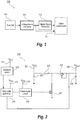
- Fig. 1 highly schematically illustrates a portable electronic device 100 according to the prior art comprising a fuel cell 101, a voltage boost converter 102, a digital signal processor (DSP) 103 and other electronic components 104.
- the fuel cell 101 provides electrical power at a relatively low voltage to the voltage boost converter 102 which in turn provides electric power at a higher voltage to the DSP (103) and the other electrical components 104 of the portable electronic device 100.
- DSP digital signal processor
- This configuration is advantageous in that the voltage boost converter takes up very little space while allowing the portable electronic device to be powered by a single low voltage fuel cell as opposed to e.g. a fuel cell stack.
- the voltage boost converter takes up very little space since it can be implemented mainly as an integrated circuit (chip) as will be further described below.
- the portable electronic device 100 is a hearing aid and the fuel cell 101 is of the direct methanol type (DMFC).
- DMFC direct methanol type
- the fuel cell 101 is of the direct alcohol type (DAFC) which is a more general term that includes DMFCs.
- DAFC direct alcohol type
- the fuel cell 101 is any low voltage power supply that is not capable of providing an output voltage of a level sufficient to operate the portable electronic device.
- the voltage boost converter comprises an input voltage terminal 201, an output voltage terminal 202, an input capacitor 203, an output capacitor 204, an inductive element 205, a first digital switch 206, a second digital switch 207, a clock boost circuit 208, a digital duty cycle generator 209, an oscillator circuit 210 with corresponding voltage terminal 211 and voltage terminals 212 and 213 for supplying electrical power to the digital duty cycle generator 209 and clock boost circuit 208 respectively.
- the fuel cell 101 When the fuel cell 101 is connected to the portable electronic device 100 a positive electric voltage is provided to the input terminal 201, the digital duty cycle generator terminal 212, the clock boost circuit terminal 213, the oscillator circuit terminal 211 and the output terminal 202.
- the electrical voltage on the output terminal 202 is not provided directly by the fuel cell 101, but as a consequence of the voltage applied to the former three terminals and the operation of the voltage boost converter 102.
- the oscillator circuit 210 provides a 32 MHz digital clock signal to the digital duty cycle generator 209, wherein an adjustable clock counter provides a frequency downscaled digital clock signal that is duty cycle modulated as a function of the magnitude of the output voltage from the voltage boost converter.
- the oscillator circuit 210 comprises an RC oscillator or another low supply voltage oscillator.
- the digital duty cycle generator 209 is adapted to operate in feedback mode and only sample the fuel cell voltage at a frequency of 100 kHz.
- the fuel cell voltage is sampled in order to being able to select an appropriate duty cycle.
- the voltage of the fuel cell is sampled using a circuit that is specifically adapted to operate at a low supply voltage, as will be further discussed below with reference to Fig. 6 .
- the voltage boost converter can be powered by the fuel cell 101 alone.
- Fig. 6 which, highly schematically, illustrates the digital duty cycle generator 209 comprising a reference voltage 601, a voltage divider comprising six resistors 602a, 602b,....602f, six pairs of comparators 603a, 603b,....603f and 604a, 604b,....604f, six AND gates 605a, 605b,....605f and an adjustable clock counter 606.
- the first comparator 603a is connected to the first (highest) electrical voltage of the voltage divider and to the fuel cell voltage and the second comparator 604a is connected to the second (next highest) electrical voltage of the voltage divider and to the fuel cell voltage.
- the output from the first and second comparators 603a and 604a are fed to the AND gate 605a.
- the comparator set 603a and 604a and the AND gate 605a are configured such that the output of the AND gate 605a will only be set to high when the fuel cell voltage is located in the interval between said first and second electric voltage.
- the other comparators and AND gates are arranged in a similar manner.
- the comparators 603a, 603b,....603f and 604a, 604b,....604f are operated at a sampling frequency of only 100 kHz, which is sufficient for following the variations of the fuel cell voltage.
- the adjustable clock counter 606 down-scales the digital clock signal from the oscillator circuit 210 from 32 MHz to 3 MHz and modulates the duty cycle of the down-scaled clock signal dependent on the determined fuel cell electrical voltage.
- This low supply voltage is partly a result of the mainly digital implementation and partly a result of the relative low frequency used for sampling the fuel cell voltage or boosted output voltage. It has been shown that the digital duty cycle generator 209 can be powered directly by a single DMFC without requiring any additional power source to aid in the start-up phase.
- phase is interchangeable with the term “mode of operation”.
- the voltage divider comprises six transistors with varying gate thresholds, that are arranged such that the electrical voltage of the fuel cell is connected to the gates of the transistors, and the electrical voltage at the transistor drains is connected to the AND gates, whereby the six resistors of the voltage divider as well as the six set of comparators can be replaced by six transistors with distinct gate thresholds.
- the number of resistors, comparator sets and AND gates can be any number in the range between two and twenty.
- the resistors, comparator sets and AND gates can be omitted if the fuel cell is developed to a level where the fuel cell output voltage dependence of the load can be kept within a very limited range such as e.g. a resulting fuel cell output voltage between 0.5 V and 0.6 V.
- the sampling frequency of the fuel cell voltage can be in the range between 100 Hz and 10 MHz and the frequency of the duty cycle modulated signal can be in the range between 100 kHz and 100 MHz.
- the frequency of the duty cycle modulated signal is switched, by the adjustable clock counter 606, between two values e.g. 5 MHz and 6 MHz.
- the range of available duty cycle values can be increased because a 5 MHz signal that is duty cycle modulated by a 30 MHz signal can provide duty cycles of 17 %, 33 %, 50 %, 66 % and 83 % and a 6 MHz signal that is duty cycle modulated by a 30 MHz signal can provide duty cycles of 20 %, 40 %, 60 % and 80 %.
- the fuel cell voltage is sampled instead of the boost converter output voltage and the boost converter is hereby operated in feed forward mode.
- the boost converter is hereby operated in feed forward mode.
- the fuel cell voltage and the boost converter output voltage include any voltage derived directly from these.
- the adjustable clock counter 606 is operated asynchronous whereby clocking of the comparators will no longer be required.
- the duty cycle modulated clock signal is provided to the clock boost circuit 213 wherein the voltage of said signal in the "high" state is increased to two times the fuel cell voltage.
- the clock boost circuit is described further below with reference to Fig. 3 and Fig. 4 .
- the voltage doubled duty cycle modulated control signal is used to drive the second digital switch 207 and as soon as the second digital switch 207 starts operating the voltage at the output terminal 202 will be boosted relative to the voltage at input terminal 201 as a consequence of the well-known principles for switched mode voltage boosting.
- the first digital switch 206 is implemented as MOSFET but not actively driven and will therefore act as a passive diode; this phenomenon may in the following be denoted to be due to the inherent body diode.
- the oscillator circuit 210 is not part of the boost voltage converter 102. Instead the digital clock signal is extracted from the portable electronic device 100. In a further variation the digital clock signal can be extracted without having to power up the remaining electronic components 104 of the portable electronic device 100.
- the output capacitor 204 has a capacitance of 5 uF
- the input capacitor 203 has a capacitance of 10 uF
- the inductive element 205 has an inductance of 10 uH. Obviously these values also depend on the selected operating frequency for the boost converter.
- the clock boost circuit 208 comprises a first inverter 301, a second inverter 302, a capacitor 303 and a first, a second and a third switch 304, 305 and 306.
- Fig. 4 illustrates the varying states of the switches in the clock boost circuit together with the voltage at selected points.
- a first state I the first switch 304 and the third switch 306 are closed and the second switch 305 is open.
- the clock signal provided from the digital duty cycle generator 209 is low (and the voltage at "a” therefore is low) the result is that the capacitor 303 will be charged.
- a second state II all three switches are open and the clock signal is "high” (and the voltage at "a” is therefore high), whereby, in a third state III, a voltage at "b” is two times the magnitude of the original clock signal and provided by closing the second switch 305.
- the voltage of the duty cycle modulated clock signal is doubled, which may be critical for operation of the voltage boost converter 102 because said clock signal is used to drive the second digital switch 207, which may require a voltage that is larger than the voltage the fuel cell can provide when it is more than lightly loaded.
- Fig. 5 which, highly schematically, illustrates a block diagram of a voltage boost converter circuit 500 according to an embodiment of the invention.
- the boost converter circuit according to the embodiment of Fig. 5 is also described with reference to the voltage boost converter of Fig. 2 .
- PWM Pulse-width Modulation
- the fuel cell 101 is lightly loaded. Most types of fuel cells will therefore, in the start-up phase, be capable of providing the voltage and electrical power required to operate the part of the voltage boost converter circuit that has already been described with reference to Fig. 2 , and to operate the selector 503, which sees to that the second switch 207 is actively driven, while the first switch 206 and the third switch 508 are not actively driven, though the first switch 206 operates as a passive diode due to the inherent body diode.
- the output from the voltage boost converter circuit is sufficient to additionally power up the Pulse-Width Modulation (PWM) generator 501 and to start actively driving said first 206 and third switch 508.
- PWM Pulse-Width Modulation
- this phase the third switch 508 is driven in-phase with the second switch 207, and the first switch 206 is driven out-of-phase.
- the first switch 206 When the first switch 206 is actively driven, it operates as a synchronous rectifier whereby the voltage loss across the switch is reduced.
- this intermediate phase is initiated by the selector 503 when it detects that the level of the boosted output voltage has reached a given trigger level, and in response hereto the selector 503 activates said first 206 and third switch 207 and the corresponding gate drivers 506 and 509.
- the PWM generator uses a down-scaled clock signal provided from the duty cycle generator 209.
- the voltage detector 513 has electrical power supplied from terminal 511 that is directly connected to the boost converter output terminal 202.
- the voltage detector 513 also monitors the voltage of the fuel cell 101 via terminal 512, thus enabling it to respond to overload conditions where the fuel cell 101 voltage may drop below a predetermined threshold.
- the second switch 207, the digital duty cycle generator 209 and the clock boost circuit 208 are first disabled or operated in a special mode in order to reduce the overall power consumption. Finally, the boost converter circuit starts to power the remaining parts of the portable electronic device.
- a fourth switch 514 which is controlled by the voltage detector, which, when activated, short-circuits the ground 515 of the remaining parts of the portable electronic device with the ground of the boost converter circuit, whereby electrical power from the boost converter circuit is provided to the remaining parts of the portable electronic device.
- the fourth switch 514 can be deactivated, thereby significantly reducing the power demands.
- the digital duty cycle generator 209 can be operated in a power saving mode where the duty cycle modulation is disabled while the digital duty cycle generator still provides a down-scaled clock signal to the PWM generator 501.
- the adjustable clock counter 606 of the digital duty cycle generator is active.
- the digital duty cycle generator 209 In a start-up phase the digital duty cycle generator 209 generates the duty cycle modulated clock signal used to drive the boost converter circuit 500.
- both the digital duty cycle generator 209 and the PWM generator 501 are active in driving the boost converter circuit 500 and in a normal mode of operation the PWM generator alone generates the duty cycle modulated clock signal used to drive the boost converter circuit 500.
- the intermediate phase is omitted and according to another variation not being covered by the scope of the claims the normal mode of operation is not exclusively controlled by the PWM generator 501.
- the PWM generator 501 is adapted such that the digital clock signal selectively can be provided from different oscillator circuits.
- an RC oscillator circuit is active in a start-up phase, in order to reduce the requirements to the supply voltage during start-up, and in a subsequent phase, the RC oscillator is replaced by a more precise crystal oscillator that requires a higher supply voltage.
- the PWM generator comprises a current generator 702, a first capacitor 703, a comparator 704, an operational amplifier 705, a second capacitor 706, a first and a second resistor 707 and 708, a first terminal 709 connected to a reference voltage and a second terminal 710 connected to the output voltage of the boost converter 500 from the embodiment of Fig. 5 .
- a downscaled digital clock signal 701 with a clock frequency of 3 MHz is input to the PWM generator 501, from the digital duty cycle generator 209, where the current generator 702 provides an alternating positive and negative bias current in response to the digital clock signal 701.
- the current generator 702 is coupled in parallel with the first capacitor 703 and the comparator 704 and therefore provides at the (negative) input of the comparator 704 a sawtooth signal.
- the other (positive) input of the comparator 704 is provided by the operational amplifier 705, which has its output coupled back, through the second capacitor 706, to the negative input of the operational amplifier 705, which also, through a first resistor, is connected to the second terminal 710.
- the positive input of the operational amplifier 705 is, through a second resistor, connected to the first terminal 709.
- the output signal 711 provided by the comparator 704 will be a square signal with a frequency that follows the frequency of the downscaled digital clock signal 701 and a duty cycle, which is higher than the nominal value when the boost converter electric voltage at the second terminal 710 is lower than the selected reference electric voltage at the first terminal 709, and wherein the duty cycle is lower than the nominal value if the boost converter electric voltage at the second terminal 710 is higher than the selected reference electric voltage at the first terminal 709.
- the comparator 704 is selected such that the bandwidth is an order of magnitude larger than the frequency of the downscaled digital clock signal 701.
- This provides a PWM generator 501 capable of generating an output signal 711 that is regulated fast and with a high resolution, whereby the output voltage from the boost converter circuit 500 according to the embodiment of Fig. 5 can be kept at the desired value with only minor deviations there from (i.e. an improved stability of the boosted voltage).
- this high quality boost converter output comes at the cost of a higher power consumption and requires a higher supply voltage level compared to the previously described digital duty cycle generator 209. This is partly because the analog operational amplifier 705 of the PWM generator 501 consumes more power and requires a higher supply voltage than the corresponding digital components used in the digital duty cycle generator 209, and partly because the bandwidth of the PWM generator 501 is considerably higher than the corresponding sampling frequency of the fuel cell voltage in the digital duty cycle generator 209.
- the boost converter circuitry 500 is further advantageous in that the normal mode of operation is a highly power efficient mode of operation. This increase in power efficiency relative to the start-up and intermediate phases is primarily due to the higher gate-source voltage (and corresponding lower on-resistance) of the switches 206, 508 and 514 that can be provided from the boosted output voltage when the boost converter circuitry 500 is operated in said normal mode.
- Another advantage of the higher gate-source voltage is the higher saturation current and hereby higher peak-power that the switches 206, 508 and 514 can provide when the boost converter circuitry 500 is operated in said normal mode.
- the boost converter circuitry 500 provides at least two modes of operation such that the circuitry selectively can be optimized with respect to either low supply voltage operation or high quality operation, wherein the high quality mode of operation is characterized by having at least one of the features: higher power efficiency, higher peak-power or more stable boosted voltage relative to the low supply voltage mode of operation.
- the high quality mode of operation may also be denoted the normal mode of operation.
- the boost converters according to the embodiments of Fig. 2 and Fig. 5 are both characterized by being based on a magnetic field storage component (the coil 205) to store the input energy temporarily and subsequently release that energy to the output at a boosted electric voltage.
- a drawback for this type of converter is the electromagnetic noise resulting from the continuously varying magnetic fields.
- Electromagnetic noise may in particular be a problem for portable electronic devices adapted for wireless communication, such as e.g. most modern hearing aids.
- the boost converter is therefore based on fixed frequency switching (duty cycle modulation) wherein the clock frequency of the duty cycle modulated control signal is selected such that the control signal and its harmonics do not interfere with a wireless communication system of the portable electronic device.
- a portable electronic device is further advantageous in that the boost converter is well suited for power management.
- the boost converter can in a simple manner lower the output voltage and hereby the current draw in response to an excessive current draw.
- the boost converter output voltage drops below a specified level this is considered to be caused by excessive power drain and therefore triggers that electrical power is no longer provided to the remaining parts of the portable electronic device.
- the instantaneous power drain is therefore dramatically reduced which allows the boost converter output voltage to recover and return to its normal nominal level whereby the remaining parts of the portable electronic device can again be powered from the boost converter.
- the boost converter increases the fuel cell output voltage to a level in the range between 1.1 and 1.6 V, or in the range between 1.3 and 1.6 V or about 1.5 V.
Landscapes
- Physics & Mathematics (AREA)
- Engineering & Computer Science (AREA)
- Acoustics & Sound (AREA)
- Signal Processing (AREA)
- Health & Medical Sciences (AREA)
- General Health & Medical Sciences (AREA)
- Neurosurgery (AREA)
- Otolaryngology (AREA)
- Dc-Dc Converters (AREA)
- Fuel Cell (AREA)
Claims (11)
- Dispositif électronique portable (100) adapté pour être porté, au moins en partie, dans ou au niveau d'une oreille humaine, comprenant une alimentation basse tension (101) fournissant une tension de sortie d'alimentation basse tension et un convertisseur amplificateur (102, 500), dans lequel ledit convertisseur amplificateur (102, 500) est adapté pour augmenter la tension de sortie d'alimentation basse tension jusqu'à un niveau approprié pour alimenter le dispositif électronique portable (100),- dans lequel ledit convertisseur amplificateur (102, 500) est alimenté par l'alimentation basse tension, dans lequel ladite alimentation basse tension (101) n'est pas capable de fournir une tension de sortie d'un niveau suffisant pour faire fonctionner le dispositif électronique portable (100)
CARACTÉRISÉ EN CE QUE- le convertisseur amplificateur (102, 500) comprend en outre un générateur de rapport cyclique numérique (209) et un générateur de modulation en largeur d'impulsions analogique (501), les deux générateurs étant configurés pour générer un signal d'horloge modulé par rapport cyclique pour entraîner le convertisseur amplificateur (102, 500),- dans lequel le générateur de rapport cyclique numérique (209) est adapté pour entraîner le convertisseur amplificateur (102, 500) avec une basse tension d'alimentation et comprend des moyens pour échantillonner la tension de sortie d'alimentation basse tension ou la tension de sortie de convertisseur amplificateur et des moyens pour ajuster le rapport cyclique d'un signal d'horloge numérique en réponse à la valeur de ladite tension échantillonnée,- dans lequel le générateur de modulation en largeur d'impulsions analogique (501) est adapté pour entraîner le convertisseur amplificateur (102, 500) avec une stabilité élevée de la tension amplifiée, et- dans lequel le convertisseur amplificateur (102, 500) est configuré pour utiliser le générateur de rapport cyclique numérique (209) pour générer le signal d'horloge modulé par rapport cyclique pour entraîner le convertisseur amplificateur (102, 500) lorsque le dispositif portable (100) est dans un mode de démarrage et pour utiliser le générateur de modulation en largeur d'impulsions analogique (501) pour générer le signal d'horloge modulé par rapport cyclique lorsque le dispositif électronique portable (100) est dans un mode de fonctionnement normal. - Dispositif électronique portable (100) selon l'une quelconque des revendications précédentes, dans lequel le convertisseur amplificateur (102, 500) comprend des moyens de déclenchement adaptés pour commuter le mode de fonctionnement entre un mode de démarrage et un mode normal en fonction du niveau de la tension amplifiée.
- Dispositif électronique portable (100) selon la revendication 2, dans lequel le convertisseur amplificateur (102, 500) est adapté pour fonctionner pendant une transition du mode de démarrage au mode normal dans un mode de fonctionnement intermédiaire.
- Dispositif électronique portable (100) selon l'une quelconque des revendications précédentes, comprenant un circuit oscillateur RC et un oscillateur à cristal.
- Dispositif électronique portable (100) selon l'une quelconque des revendications 1 à 4, dans lequel le générateur de modulation en largeur d'impulsions est actionné dans une configuration de rétroaction.
- Dispositif électronique portable (100) selon l'une quelconque des revendications 1 à 4, dans lequel le générateur de rapport cyclique numérique (209) échantillonne la tension d'alimentation basse tension ou la tension de sortie de convertisseur amplificateur à une fréquence dans la plage entre 100 Hz et 10 MHz, et dans lequel le générateur de modulation en largeur d'impulsions (501) est adapté pour fournir une largeur de bande qui est au moins d'un facteur 5 fois supérieur à la fréquence du signal d'horloge délivré en sortie par le générateur de modulation en largeur d'impulsions.
- Dispositif électronique portable (100) selon l'une quelconque des revendications 1 à 4, dans lequel le générateur de rapport cyclique numérique (209) est adapté pour fournir une tension amplifiée à un premier niveau et dans lequel le générateur de modulation en largeur d'impulsions (501) est adapté pour fournir une tension amplifiée à un second niveau, dans lequel ledit second niveau est plus grand que ledit premier niveau, selon lequel une simple détection de tension est utilisée pour déterminer si le convertisseur amplificateur (102, 500) est prêt à fournir une tension aux parties restantes du dispositif électronique portable.
- Dispositif électronique portable (100) selon l'une quelconque des revendications 1 à 4, dans lequel lesdits moyens d'échantillonnage comprennent deux transistors avec des seuils de grille de transistor distincts, qui sont agencés de telle sorte que ladite tension à échantillonner est connectée aux grilles des transistors et la tension au niveau des drains de transistor est connectée à une porte logique, selon lequel la sortie de la porte logique est utilisée pour déterminer la valeur de ladite tension par rapport aux deux seuils de grille de transistor.
- Dispositif électronique portable (100) selon l'une quelconque des revendications précédentes, dans lequel le dispositif électronique portable est une aide auditive.
- Dispositif électronique portable (100) selon l'une quelconque des revendications précédentes, dans lequel l'alimentation basse tension est une pile directe à combustible à alcool.
- Procédé de fonctionnement d'un dispositif électronique portable (100) comprenant les étapes consistant à :- fournir une alimentation basse tension (101) fournissant une tension de sortie d'alimentation basse tension, dans lequel ladite alimentation basse tension (101) n'est pas capable de fournir une tension de sortie d'un niveau suffisant pour faire fonctionner le dispositif électronique portable (100) et- fournir un convertisseur amplificateur (102, 500) adapté pour augmenter la tension de sortie d'alimentation basse tension à un niveau approprié pour alimenter le dispositif électronique portable (100) et dans lequel ledit convertisseur amplificateur (102, 500) est alimenté par l'alimentation basse tension (101), CARACTÉRISÉ PAR- fournir un générateur de rapport cyclique numérique (209), et un générateur de modulation en largeur d'impulsions analogique (501), les deux générateurs étant configurés pour générer un signal d'horloge modulé par rapport cyclique pour entraîner le convertisseur amplificateur (102, 500),- entraîner le convertisseur amplificateur (102, 500) avec une basse tension d'alimentation en utilisant un générateur de rapport cyclique numérique (209) adapté pour échantillonner la tension de sortie d'alimentation basse tension ou une tension de sortie de convertisseur amplificateur et ajuster le rapport cyclique d'un signal d'horloge numérique en réponse à la valeur de la tension échantillonnée,- entraîner le convertisseur amplificateur (102, 500) avec une stabilité élevée de la tension amplifiée en utilisant le générateur de modulation en largeur d'impulsions analogique (501),- utiliser le générateur de rapport cyclique numérique (209) pour générer le signal d'horloge modulé par rapport cyclique pour entraîner le convertisseur amplificateur (102, 500) lorsque le dispositif portable (100) est dans un mode de démarrage, et- utiliser le générateur de modulation en largeur d'impulsions analogique (501) pour générer le signal d'horloge modulé par rapport cyclique lorsque le dispositif électronique portable (100) est dans un mode de fonctionnement normal.
Applications Claiming Priority (1)
| Application Number | Priority Date | Filing Date | Title |
|---|---|---|---|
| PCT/EP2011/073030 WO2013087118A1 (fr) | 2011-12-16 | 2011-12-16 | Dispositif électronique portable à porter à l'oreille et procédé de fonctionnement d'un dispositif électronique portable |
Publications (2)
| Publication Number | Publication Date |
|---|---|
| EP2792166A1 EP2792166A1 (fr) | 2014-10-22 |
| EP2792166B1 true EP2792166B1 (fr) | 2021-10-06 |
Family
ID=45375306
Family Applications (1)
| Application Number | Title | Priority Date | Filing Date |
|---|---|---|---|
| EP11799283.4A Active EP2792166B1 (fr) | 2011-12-16 | 2011-12-16 | Dispositif électronique portable à porter à l'oreille et procédé de fonctionnement d'un dispositif électronique portable |
Country Status (4)
| Country | Link |
|---|---|
| US (1) | US9344812B2 (fr) |
| EP (1) | EP2792166B1 (fr) |
| DK (1) | DK2792166T3 (fr) |
| WO (1) | WO2013087118A1 (fr) |
Families Citing this family (6)
| Publication number | Priority date | Publication date | Assignee | Title |
|---|---|---|---|---|
| JP2015073167A (ja) * | 2013-10-02 | 2015-04-16 | 日東電工株式会社 | 補聴器及び補聴器充電システム |
| JP6604708B2 (ja) * | 2013-10-02 | 2019-11-13 | 日東電工株式会社 | 補聴器 |
| US11695283B2 (en) * | 2018-05-11 | 2023-07-04 | Texas Instruments Incorporated | Shoot-through current limiting circuit |
| US12496328B2 (en) * | 2018-07-20 | 2025-12-16 | Association Institut De Myologie | Compositions for the treatment of sarcopenia or disuse atrophy |
| EP4315884A1 (fr) * | 2021-03-24 | 2024-02-07 | Widex A/S | Dispositif audio à niveau d'oreille et procédé de fonctionnement d'un dispositif audio à niveau d'oreille |
| TWI791257B (zh) * | 2021-08-02 | 2023-02-01 | 群聯電子股份有限公司 | 訊號重驅動裝置、資料儲存系統及模式控制方法 |
Family Cites Families (4)
| Publication number | Priority date | Publication date | Assignee | Title |
|---|---|---|---|---|
| WO2002067628A1 (fr) | 2001-02-17 | 2002-08-29 | Oticon A/S | Dispositif de communication a monter sur ou dans l'oreille |
| DE10115429A1 (de) | 2001-03-29 | 2002-05-02 | Siemens Audiologische Technik | Hörgerät |
| DK1432286T3 (da) * | 2004-01-12 | 2011-02-21 | Phonak Ag | Høreapparat med brændstofcelle |
| US8031878B2 (en) * | 2005-07-28 | 2011-10-04 | Bose Corporation | Electronic interfacing with a head-mounted device |
-
2011
- 2011-12-16 EP EP11799283.4A patent/EP2792166B1/fr active Active
- 2011-12-16 WO PCT/EP2011/073030 patent/WO2013087118A1/fr not_active Ceased
- 2011-12-16 DK DK11799283.4T patent/DK2792166T3/da active
- 2011-12-16 US US14/237,389 patent/US9344812B2/en active Active
Non-Patent Citations (1)
| Title |
|---|
| None * |
Also Published As
| Publication number | Publication date |
|---|---|
| WO2013087118A1 (fr) | 2013-06-20 |
| US9344812B2 (en) | 2016-05-17 |
| US20140233776A1 (en) | 2014-08-21 |
| DK2792166T3 (da) | 2021-10-25 |
| EP2792166A1 (fr) | 2014-10-22 |
Similar Documents
| Publication | Publication Date | Title |
|---|---|---|
| EP2792166B1 (fr) | Dispositif électronique portable à porter à l'oreille et procédé de fonctionnement d'un dispositif électronique portable | |
| EP3319215B1 (fr) | Instrument auditif comprenant un convertisseur de puissance cc-cc à condensateur commuté | |
| CN106463987B (zh) | 用于听力仪器中的银锌电池的电压调节器及控制电路 | |
| JP2019115252A (ja) | 外部および内部フライングキャパシタを備えるスイッチトキャパシタdc−dc変換器 | |
| JP2018107963A (ja) | エナジーハーベスト端末 | |
| US20240381040A1 (en) | Hearing device having a power source | |
| CN112202234B (zh) | 一种电源管理电路和电子设备 | |
| EP3491726B1 (fr) | Circuit intégré de gestion de puissance avec démarrage à froid programmable | |
| US6829364B2 (en) | Hearing aid with a capacitor having a large capacitance | |
| US20110103628A1 (en) | Hearing device and method for operating the same | |
| TW571494B (en) | Micro power supply with integrated charging capability | |
| US20190165671A1 (en) | Switched capacitor voltage converter for a rechargeable battery in a hearing aid | |
| CN110324771A (zh) | 麦克风阵列 | |
| EP1272001B1 (fr) | Prothèse auditive avec condensateur de grande capacité | |
| US20180227680A1 (en) | Acoustic Power Coupling for Mobile Audio Devices | |
| US8362747B2 (en) | Method of powering a mobile device | |
| US20240171071A1 (en) | An ear level audio device and a method of operating an ear level audio device | |
| CN118263917B (zh) | 电池控制系统、方法和装置 | |
| EP4492823A1 (fr) | Dispositif auditif avec convertisseur continu-continu à entrées multiples et sorties multiples | |
| CN112713661A (zh) | 无线反向充电的信号发射系统及电子设备 | |
| KR20090066108A (ko) | 배터리 전압 증폭 장치 및 그 제어 방법 | |
| WO2023033738A1 (fr) | Mécanisme de protection pour système récepteur de charge sans fil | |
| EP3179741B1 (fr) | Prothèse auditive à gestion d'énergie | |
| CN118433621A (zh) | 用于运行听力设备的方法 | |
| CN202616835U (zh) | 充电控制电路 |
Legal Events
| Date | Code | Title | Description |
|---|---|---|---|
| PUAI | Public reference made under article 153(3) epc to a published international application that has entered the european phase |
Free format text: ORIGINAL CODE: 0009012 |
|
| 17P | Request for examination filed |
Effective date: 20140716 |
|
| AK | Designated contracting states |
Kind code of ref document: A1 Designated state(s): AL AT BE BG CH CY CZ DE DK EE ES FI FR GB GR HR HU IE IS IT LI LT LU LV MC MK MT NL NO PL PT RO RS SE SI SK SM TR |
|
| DAX | Request for extension of the european patent (deleted) | ||
| RAP1 | Party data changed (applicant data changed or rights of an application transferred) |
Owner name: TEKNOLOGISK INSTITUT |
|
| STAA | Information on the status of an ep patent application or granted ep patent |
Free format text: STATUS: EXAMINATION IS IN PROGRESS |
|
| 17Q | First examination report despatched |
Effective date: 20170403 |
|
| GRAP | Despatch of communication of intention to grant a patent |
Free format text: ORIGINAL CODE: EPIDOSNIGR1 |
|
| STAA | Information on the status of an ep patent application or granted ep patent |
Free format text: STATUS: GRANT OF PATENT IS INTENDED |
|
| INTG | Intention to grant announced |
Effective date: 20210729 |
|
| RIN1 | Information on inventor provided before grant (corrected) |
Inventor name: KROGSGAARD, KLAUS Inventor name: LUND-OLESEN, TORSTEN Inventor name: KALLESOEE, CHRISTIAN Inventor name: HALES, JAN HARRY Inventor name: CHRISTENSEN, LEIF HOEJSLET Inventor name: KIDMOSE, PREBEN |
|
| GRAS | Grant fee paid |
Free format text: ORIGINAL CODE: EPIDOSNIGR3 |
|
| GRAA | (expected) grant |
Free format text: ORIGINAL CODE: 0009210 |
|
| STAA | Information on the status of an ep patent application or granted ep patent |
Free format text: STATUS: THE PATENT HAS BEEN GRANTED |
|
| AK | Designated contracting states |
Kind code of ref document: B1 Designated state(s): AL AT BE BG CH CY CZ DE DK EE ES FI FR GB GR HR HU IE IS IT LI LT LU LV MC MK MT NL NO PL PT RO RS SE SI SK SM TR |
|
| REG | Reference to a national code |
Ref country code: GB Ref legal event code: FG4D |
|
| REG | Reference to a national code |
Ref country code: CH Ref legal event code: EP Ref country code: AT Ref legal event code: REF Ref document number: 1437282 Country of ref document: AT Kind code of ref document: T Effective date: 20211015 |
|
| REG | Reference to a national code |
Ref country code: DE Ref legal event code: R096 Ref document number: 602011071898 Country of ref document: DE |
|
| REG | Reference to a national code |
Ref country code: DK Ref legal event code: T3 Effective date: 20211021 |
|
| REG | Reference to a national code |
Ref country code: IE Ref legal event code: FG4D |
|
| REG | Reference to a national code |
Ref country code: LT Ref legal event code: MG9D |
|
| REG | Reference to a national code |
Ref country code: NL Ref legal event code: MP Effective date: 20211006 |
|
| REG | Reference to a national code |
Ref country code: AT Ref legal event code: MK05 Ref document number: 1437282 Country of ref document: AT Kind code of ref document: T Effective date: 20211006 |
|
| PG25 | Lapsed in a contracting state [announced via postgrant information from national office to epo] |
Ref country code: RS Free format text: LAPSE BECAUSE OF FAILURE TO SUBMIT A TRANSLATION OF THE DESCRIPTION OR TO PAY THE FEE WITHIN THE PRESCRIBED TIME-LIMIT Effective date: 20211006 Ref country code: LT Free format text: LAPSE BECAUSE OF FAILURE TO SUBMIT A TRANSLATION OF THE DESCRIPTION OR TO PAY THE FEE WITHIN THE PRESCRIBED TIME-LIMIT Effective date: 20211006 Ref country code: FI Free format text: LAPSE BECAUSE OF FAILURE TO SUBMIT A TRANSLATION OF THE DESCRIPTION OR TO PAY THE FEE WITHIN THE PRESCRIBED TIME-LIMIT Effective date: 20211006 Ref country code: BG Free format text: LAPSE BECAUSE OF FAILURE TO SUBMIT A TRANSLATION OF THE DESCRIPTION OR TO PAY THE FEE WITHIN THE PRESCRIBED TIME-LIMIT Effective date: 20220106 Ref country code: AT Free format text: LAPSE BECAUSE OF FAILURE TO SUBMIT A TRANSLATION OF THE DESCRIPTION OR TO PAY THE FEE WITHIN THE PRESCRIBED TIME-LIMIT Effective date: 20211006 |
|
| PG25 | Lapsed in a contracting state [announced via postgrant information from national office to epo] |
Ref country code: IS Free format text: LAPSE BECAUSE OF FAILURE TO SUBMIT A TRANSLATION OF THE DESCRIPTION OR TO PAY THE FEE WITHIN THE PRESCRIBED TIME-LIMIT Effective date: 20220206 Ref country code: SE Free format text: LAPSE BECAUSE OF FAILURE TO SUBMIT A TRANSLATION OF THE DESCRIPTION OR TO PAY THE FEE WITHIN THE PRESCRIBED TIME-LIMIT Effective date: 20211006 Ref country code: PT Free format text: LAPSE BECAUSE OF FAILURE TO SUBMIT A TRANSLATION OF THE DESCRIPTION OR TO PAY THE FEE WITHIN THE PRESCRIBED TIME-LIMIT Effective date: 20220207 Ref country code: PL Free format text: LAPSE BECAUSE OF FAILURE TO SUBMIT A TRANSLATION OF THE DESCRIPTION OR TO PAY THE FEE WITHIN THE PRESCRIBED TIME-LIMIT Effective date: 20211006 Ref country code: NO Free format text: LAPSE BECAUSE OF FAILURE TO SUBMIT A TRANSLATION OF THE DESCRIPTION OR TO PAY THE FEE WITHIN THE PRESCRIBED TIME-LIMIT Effective date: 20220106 Ref country code: NL Free format text: LAPSE BECAUSE OF FAILURE TO SUBMIT A TRANSLATION OF THE DESCRIPTION OR TO PAY THE FEE WITHIN THE PRESCRIBED TIME-LIMIT Effective date: 20211006 Ref country code: LV Free format text: LAPSE BECAUSE OF FAILURE TO SUBMIT A TRANSLATION OF THE DESCRIPTION OR TO PAY THE FEE WITHIN THE PRESCRIBED TIME-LIMIT Effective date: 20211006 Ref country code: HR Free format text: LAPSE BECAUSE OF FAILURE TO SUBMIT A TRANSLATION OF THE DESCRIPTION OR TO PAY THE FEE WITHIN THE PRESCRIBED TIME-LIMIT Effective date: 20211006 Ref country code: GR Free format text: LAPSE BECAUSE OF FAILURE TO SUBMIT A TRANSLATION OF THE DESCRIPTION OR TO PAY THE FEE WITHIN THE PRESCRIBED TIME-LIMIT Effective date: 20220107 Ref country code: ES Free format text: LAPSE BECAUSE OF FAILURE TO SUBMIT A TRANSLATION OF THE DESCRIPTION OR TO PAY THE FEE WITHIN THE PRESCRIBED TIME-LIMIT Effective date: 20211006 |
|
| REG | Reference to a national code |
Ref country code: DE Ref legal event code: R097 Ref document number: 602011071898 Country of ref document: DE |
|
| PG25 | Lapsed in a contracting state [announced via postgrant information from national office to epo] |
Ref country code: SM Free format text: LAPSE BECAUSE OF FAILURE TO SUBMIT A TRANSLATION OF THE DESCRIPTION OR TO PAY THE FEE WITHIN THE PRESCRIBED TIME-LIMIT Effective date: 20211006 Ref country code: SK Free format text: LAPSE BECAUSE OF FAILURE TO SUBMIT A TRANSLATION OF THE DESCRIPTION OR TO PAY THE FEE WITHIN THE PRESCRIBED TIME-LIMIT Effective date: 20211006 Ref country code: RO Free format text: LAPSE BECAUSE OF FAILURE TO SUBMIT A TRANSLATION OF THE DESCRIPTION OR TO PAY THE FEE WITHIN THE PRESCRIBED TIME-LIMIT Effective date: 20211006 Ref country code: MC Free format text: LAPSE BECAUSE OF FAILURE TO SUBMIT A TRANSLATION OF THE DESCRIPTION OR TO PAY THE FEE WITHIN THE PRESCRIBED TIME-LIMIT Effective date: 20211006 Ref country code: EE Free format text: LAPSE BECAUSE OF FAILURE TO SUBMIT A TRANSLATION OF THE DESCRIPTION OR TO PAY THE FEE WITHIN THE PRESCRIBED TIME-LIMIT Effective date: 20211006 Ref country code: CZ Free format text: LAPSE BECAUSE OF FAILURE TO SUBMIT A TRANSLATION OF THE DESCRIPTION OR TO PAY THE FEE WITHIN THE PRESCRIBED TIME-LIMIT Effective date: 20211006 |
|
| PLBE | No opposition filed within time limit |
Free format text: ORIGINAL CODE: 0009261 |
|
| STAA | Information on the status of an ep patent application or granted ep patent |
Free format text: STATUS: NO OPPOSITION FILED WITHIN TIME LIMIT |
|
| 26N | No opposition filed |
Effective date: 20220707 |
|
| REG | Reference to a national code |
Ref country code: BE Ref legal event code: MM Effective date: 20211231 |
|
| PG25 | Lapsed in a contracting state [announced via postgrant information from national office to epo] |
Ref country code: LU Free format text: LAPSE BECAUSE OF NON-PAYMENT OF DUE FEES Effective date: 20211216 Ref country code: IE Free format text: LAPSE BECAUSE OF NON-PAYMENT OF DUE FEES Effective date: 20211216 Ref country code: AL Free format text: LAPSE BECAUSE OF FAILURE TO SUBMIT A TRANSLATION OF THE DESCRIPTION OR TO PAY THE FEE WITHIN THE PRESCRIBED TIME-LIMIT Effective date: 20211006 |
|
| PG25 | Lapsed in a contracting state [announced via postgrant information from national office to epo] |
Ref country code: SI Free format text: LAPSE BECAUSE OF FAILURE TO SUBMIT A TRANSLATION OF THE DESCRIPTION OR TO PAY THE FEE WITHIN THE PRESCRIBED TIME-LIMIT Effective date: 20211006 Ref country code: BE Free format text: LAPSE BECAUSE OF NON-PAYMENT OF DUE FEES Effective date: 20211231 |
|
| PG25 | Lapsed in a contracting state [announced via postgrant information from national office to epo] |
Ref country code: IT Free format text: LAPSE BECAUSE OF FAILURE TO SUBMIT A TRANSLATION OF THE DESCRIPTION OR TO PAY THE FEE WITHIN THE PRESCRIBED TIME-LIMIT Effective date: 20211006 Ref country code: HU Free format text: LAPSE BECAUSE OF FAILURE TO SUBMIT A TRANSLATION OF THE DESCRIPTION OR TO PAY THE FEE WITHIN THE PRESCRIBED TIME-LIMIT; INVALID AB INITIO Effective date: 20111216 Ref country code: CY Free format text: LAPSE BECAUSE OF FAILURE TO SUBMIT A TRANSLATION OF THE DESCRIPTION OR TO PAY THE FEE WITHIN THE PRESCRIBED TIME-LIMIT Effective date: 20211006 |
|
| PG25 | Lapsed in a contracting state [announced via postgrant information from national office to epo] |
Ref country code: MK Free format text: LAPSE BECAUSE OF FAILURE TO SUBMIT A TRANSLATION OF THE DESCRIPTION OR TO PAY THE FEE WITHIN THE PRESCRIBED TIME-LIMIT Effective date: 20211006 |
|
| PG25 | Lapsed in a contracting state [announced via postgrant information from national office to epo] |
Ref country code: TR Free format text: LAPSE BECAUSE OF FAILURE TO SUBMIT A TRANSLATION OF THE DESCRIPTION OR TO PAY THE FEE WITHIN THE PRESCRIBED TIME-LIMIT Effective date: 20211006 |
|
| PG25 | Lapsed in a contracting state [announced via postgrant information from national office to epo] |
Ref country code: MT Free format text: LAPSE BECAUSE OF FAILURE TO SUBMIT A TRANSLATION OF THE DESCRIPTION OR TO PAY THE FEE WITHIN THE PRESCRIBED TIME-LIMIT Effective date: 20211006 |
|
| REG | Reference to a national code |
Ref country code: CH Ref legal event code: U11 Free format text: ST27 STATUS EVENT CODE: U-0-0-U10-U11 (AS PROVIDED BY THE NATIONAL OFFICE) Effective date: 20260101 |
|
| PGFP | Annual fee paid to national office [announced via postgrant information from national office to epo] |
Ref country code: DE Payment date: 20251126 Year of fee payment: 15 |
|
| PGFP | Annual fee paid to national office [announced via postgrant information from national office to epo] |
Ref country code: GB Payment date: 20251119 Year of fee payment: 15 |
|
| PGFP | Annual fee paid to national office [announced via postgrant information from national office to epo] |
Ref country code: DK Payment date: 20251119 Year of fee payment: 15 |
|
| PGFP | Annual fee paid to national office [announced via postgrant information from national office to epo] |
Ref country code: FR Payment date: 20251120 Year of fee payment: 15 |
|
| PGFP | Annual fee paid to national office [announced via postgrant information from national office to epo] |
Ref country code: CH Payment date: 20260101 Year of fee payment: 15 |