EP2793256A2 - Halbleiterbaulement und zugehörige Herstellungsmethode - Google Patents
Halbleiterbaulement und zugehörige Herstellungsmethode Download PDFInfo
- Publication number
- EP2793256A2 EP2793256A2 EP20140164833 EP14164833A EP2793256A2 EP 2793256 A2 EP2793256 A2 EP 2793256A2 EP 20140164833 EP20140164833 EP 20140164833 EP 14164833 A EP14164833 A EP 14164833A EP 2793256 A2 EP2793256 A2 EP 2793256A2
- Authority
- EP
- European Patent Office
- Prior art keywords
- terminals
- resin case
- semiconductor device
- resin
- molding die
- Prior art date
- Legal status (The legal status is an assumption and is not a legal conclusion. Google has not performed a legal analysis and makes no representation as to the accuracy of the status listed.)
- Granted
Links
Images





Classifications
-
- H—ELECTRICITY
- H10—SEMICONDUCTOR DEVICES; ELECTRIC SOLID-STATE DEVICES NOT OTHERWISE PROVIDED FOR
- H10W—GENERIC PACKAGES, INTERCONNECTIONS, CONNECTORS OR OTHER CONSTRUCTIONAL DETAILS OF DEVICES COVERED BY CLASS H10
- H10W74/00—Encapsulations, e.g. protective coatings
- H10W74/01—Manufacture or treatment
- H10W74/012—Manufacture or treatment of encapsulations on active surfaces of flip-chip devices, e.g. forming underfills
-
- H—ELECTRICITY
- H10—SEMICONDUCTOR DEVICES; ELECTRIC SOLID-STATE DEVICES NOT OTHERWISE PROVIDED FOR
- H10W—GENERIC PACKAGES, INTERCONNECTIONS, CONNECTORS OR OTHER CONSTRUCTIONAL DETAILS OF DEVICES COVERED BY CLASS H10
- H10W46/00—Marks applied to devices, e.g. for alignment or identification
-
- H—ELECTRICITY
- H10—SEMICONDUCTOR DEVICES; ELECTRIC SOLID-STATE DEVICES NOT OTHERWISE PROVIDED FOR
- H10W—GENERIC PACKAGES, INTERCONNECTIONS, CONNECTORS OR OTHER CONSTRUCTIONAL DETAILS OF DEVICES COVERED BY CLASS H10
- H10W74/00—Encapsulations, e.g. protective coatings
- H10W74/01—Manufacture or treatment
- H10W74/016—Manufacture or treatment using moulds
-
- H—ELECTRICITY
- H10—SEMICONDUCTOR DEVICES; ELECTRIC SOLID-STATE DEVICES NOT OTHERWISE PROVIDED FOR
- H10W—GENERIC PACKAGES, INTERCONNECTIONS, CONNECTORS OR OTHER CONSTRUCTIONAL DETAILS OF DEVICES COVERED BY CLASS H10
- H10W74/00—Encapsulations, e.g. protective coatings
- H10W74/10—Encapsulations, e.g. protective coatings characterised by their shape or disposition
- H10W74/15—Encapsulations, e.g. protective coatings characterised by their shape or disposition on active surfaces of flip-chip devices, e.g. underfills
-
- H—ELECTRICITY
- H10—SEMICONDUCTOR DEVICES; ELECTRIC SOLID-STATE DEVICES NOT OTHERWISE PROVIDED FOR
- H10W—GENERIC PACKAGES, INTERCONNECTIONS, CONNECTORS OR OTHER CONSTRUCTIONAL DETAILS OF DEVICES COVERED BY CLASS H10
- H10W76/00—Containers; Fillings or auxiliary members therefor; Seals
- H10W76/10—Containers or parts thereof
- H10W76/12—Containers or parts thereof characterised by their shape
- H10W76/15—Containers comprising an insulating or insulated base
- H10W76/157—Containers comprising an insulating or insulated base having interconnections parallel to the insulating or insulated base
-
- H—ELECTRICITY
- H10—SEMICONDUCTOR DEVICES; ELECTRIC SOLID-STATE DEVICES NOT OTHERWISE PROVIDED FOR
- H10W—GENERIC PACKAGES, INTERCONNECTIONS, CONNECTORS OR OTHER CONSTRUCTIONAL DETAILS OF DEVICES COVERED BY CLASS H10
- H10W90/00—Package configurations
-
- H—ELECTRICITY
- H10—SEMICONDUCTOR DEVICES; ELECTRIC SOLID-STATE DEVICES NOT OTHERWISE PROVIDED FOR
- H10W—GENERIC PACKAGES, INTERCONNECTIONS, CONNECTORS OR OTHER CONSTRUCTIONAL DETAILS OF DEVICES COVERED BY CLASS H10
- H10W46/00—Marks applied to devices, e.g. for alignment or identification
- H10W46/301—Marks applied to devices, e.g. for alignment or identification for alignment
-
- H—ELECTRICITY
- H10—SEMICONDUCTOR DEVICES; ELECTRIC SOLID-STATE DEVICES NOT OTHERWISE PROVIDED FOR
- H10W—GENERIC PACKAGES, INTERCONNECTIONS, CONNECTORS OR OTHER CONSTRUCTIONAL DETAILS OF DEVICES COVERED BY CLASS H10
- H10W46/00—Marks applied to devices, e.g. for alignment or identification
- H10W46/601—Marks applied to devices, e.g. for alignment or identification for use after dicing
- H10W46/607—Located on parts of packages, e.g. on encapsulations or on package substrates
-
- H—ELECTRICITY
- H10—SEMICONDUCTOR DEVICES; ELECTRIC SOLID-STATE DEVICES NOT OTHERWISE PROVIDED FOR
- H10W—GENERIC PACKAGES, INTERCONNECTIONS, CONNECTORS OR OTHER CONSTRUCTIONAL DETAILS OF DEVICES COVERED BY CLASS H10
- H10W70/00—Package substrates; Interposers; Redistribution layers [RDL]
- H10W70/40—Leadframes
- H10W70/479—Leadframes on or in insulating or insulated package substrates, interposers, or redistribution layers
-
- H—ELECTRICITY
- H10—SEMICONDUCTOR DEVICES; ELECTRIC SOLID-STATE DEVICES NOT OTHERWISE PROVIDED FOR
- H10W—GENERIC PACKAGES, INTERCONNECTIONS, CONNECTORS OR OTHER CONSTRUCTIONAL DETAILS OF DEVICES COVERED BY CLASS H10
- H10W72/00—Interconnections or connectors in packages
- H10W72/071—Connecting or disconnecting
- H10W72/075—Connecting or disconnecting of bond wires
-
- H—ELECTRICITY
- H10—SEMICONDUCTOR DEVICES; ELECTRIC SOLID-STATE DEVICES NOT OTHERWISE PROVIDED FOR
- H10W—GENERIC PACKAGES, INTERCONNECTIONS, CONNECTORS OR OTHER CONSTRUCTIONAL DETAILS OF DEVICES COVERED BY CLASS H10
- H10W72/00—Interconnections or connectors in packages
- H10W72/30—Die-attach connectors
- H10W72/351—Materials of die-attach connectors
- H10W72/352—Materials of die-attach connectors comprising metals or metalloids, e.g. solders
-
- H—ELECTRICITY
- H10—SEMICONDUCTOR DEVICES; ELECTRIC SOLID-STATE DEVICES NOT OTHERWISE PROVIDED FOR
- H10W—GENERIC PACKAGES, INTERCONNECTIONS, CONNECTORS OR OTHER CONSTRUCTIONAL DETAILS OF DEVICES COVERED BY CLASS H10
- H10W72/00—Interconnections or connectors in packages
- H10W72/50—Bond wires
-
- H—ELECTRICITY
- H10—SEMICONDUCTOR DEVICES; ELECTRIC SOLID-STATE DEVICES NOT OTHERWISE PROVIDED FOR
- H10W—GENERIC PACKAGES, INTERCONNECTIONS, CONNECTORS OR OTHER CONSTRUCTIONAL DETAILS OF DEVICES COVERED BY CLASS H10
- H10W72/00—Interconnections or connectors in packages
- H10W72/851—Dispositions of multiple connectors or interconnections
- H10W72/874—On different surfaces
- H10W72/884—Die-attach connectors and bond wires
-
- H—ELECTRICITY
- H10—SEMICONDUCTOR DEVICES; ELECTRIC SOLID-STATE DEVICES NOT OTHERWISE PROVIDED FOR
- H10W—GENERIC PACKAGES, INTERCONNECTIONS, CONNECTORS OR OTHER CONSTRUCTIONAL DETAILS OF DEVICES COVERED BY CLASS H10
- H10W74/00—Encapsulations, e.g. protective coatings
-
- H—ELECTRICITY
- H10—SEMICONDUCTOR DEVICES; ELECTRIC SOLID-STATE DEVICES NOT OTHERWISE PROVIDED FOR
- H10W—GENERIC PACKAGES, INTERCONNECTIONS, CONNECTORS OR OTHER CONSTRUCTIONAL DETAILS OF DEVICES COVERED BY CLASS H10
- H10W76/00—Containers; Fillings or auxiliary members therefor; Seals
- H10W76/40—Fillings or auxiliary members in containers, e.g. centering rings
- H10W76/42—Fillings
- H10W76/47—Solid or gel fillings
-
- H—ELECTRICITY
- H10—SEMICONDUCTOR DEVICES; ELECTRIC SOLID-STATE DEVICES NOT OTHERWISE PROVIDED FOR
- H10W—GENERIC PACKAGES, INTERCONNECTIONS, CONNECTORS OR OTHER CONSTRUCTIONAL DETAILS OF DEVICES COVERED BY CLASS H10
- H10W90/00—Package configurations
- H10W90/701—Package configurations characterised by the relative positions of pads or connectors relative to package parts
- H10W90/731—Package configurations characterised by the relative positions of pads or connectors relative to package parts of die-attach connectors
- H10W90/734—Package configurations characterised by the relative positions of pads or connectors relative to package parts of die-attach connectors between a chip and a stacked insulating package substrate, interposer or RDL
-
- H—ELECTRICITY
- H10—SEMICONDUCTOR DEVICES; ELECTRIC SOLID-STATE DEVICES NOT OTHERWISE PROVIDED FOR
- H10W—GENERIC PACKAGES, INTERCONNECTIONS, CONNECTORS OR OTHER CONSTRUCTIONAL DETAILS OF DEVICES COVERED BY CLASS H10
- H10W90/00—Package configurations
- H10W90/701—Package configurations characterised by the relative positions of pads or connectors relative to package parts
- H10W90/751—Package configurations characterised by the relative positions of pads or connectors relative to package parts of bond wires
- H10W90/756—Package configurations characterised by the relative positions of pads or connectors relative to package parts of bond wires between a chip and a stacked lead frame, conducting package substrate or heat sink
Definitions
- the present invention relates to a semiconductor device manufacturing method and semiconductor device.
- the invention relates to a semiconductor device manufacturing method whereby an insulating circuit substrate on which is mounted a semiconductor element is housed inside a resin case, and a terminal is integrally molded with the resin case.
- a semiconductor module wherein a plurality of a power semiconductor element such as an insulated gate bipolar transistor (IGBT) or free wheeling diode (FWD) are housed inside a resin case is known as a semiconductor device that controls a motor or the like.
- this semiconductor module is such that a power semiconductor element is mounted on an insulating circuit substrate.
- the insulating circuit substrate is such that an electrical circuit formed of a conductive layer is formed on a surface of an insulating substrate, and the power semiconductor element is electrically connected via a solder to the electrical circuit.
- the insulating circuit substrate on which is mounted the power semiconductor element is housed inside a resin case.
- a terminal is provided in the resin case.
- the conductive layer electrical circuit of the insulating circuit substrate, or the power semiconductor element, is electrically connected with a bonding wire to the terminal.
- the terminal can be electrically connected as a main terminal or control terminal to the exterior of the resin case.
- the insulating circuit substrate on which the power semiconductor element is mounted is joined to the resin case with an adhesive. A sealing resin is injected into the resin case, and moisture and the like is prevented by the sealing resin from entering the resin case, thus protecting the power semiconductor element and the like.
- the terminal is of an L-form having a leg portion.
- the resin case is of a box form having a side wall portion provided on each of four sides.
- the L-form terminal is provided in the resin case so that a leading end portion of the terminal is exposed from an upper end of the side wall portion of the resin case and the leg portion of the terminal is exposed on the inner surface side of the side wall portion of the resin case.
- the number and positions of terminals in the side wall portion of the resin case differ for each semiconductor module product.
- a terminal member wherein terminals are connected by a tie bar to a number and positions corresponding to one side wall portion of the resin case is prepared for each side wall of the resin case by carrying out a punching process and bending process on a thin plate of a conductive material, such as a copper plate.
- the terminal members are positioned to correspond to each of the side walls of the resin case in a molding die in which the resin case is to be molded, and the terminals are insert molded integrally with the resin case by a raw material resin such as a polyphenylene sulfide (PPS) resin being injected into the molding die and hardened. After molding, the tie bar is cut off.
- PPS polyphenylene sulfide
- the terminal member is of a configuration wherein the terminals are connected by the tie bar so as to be in predetermined positions, because of which unnecessary portions between terminals are thrown away in the punching process. Consequently, the proportion of the portion of the thin plate of conductive material used for the terminals is low, and the terminal cost is high. Also, when manufacturing resin cases with differing terminal layouts, it is necessary to separately prepare different molding dies in accordance with the number and positions of the terminals, and the molding die cost is high because of the need to prepare a plurality of molding dies.
- Another method of manufacturing a resin case wherein terminals are provided integrally is such that terminal attachment holes are formed in a side wall portion of the resin case in the resin case molding step so as to be compatible with all terminal arrays differing in accordance with model and specifications, and individual terminals are press fitted in predetermined positions into the attachment holes formed ( JP-A-2008-252055 (Description of the Background Art, Claims)) .
- one resin case molding die is sufficient even when manufacturing resin cases with differing terminal numbers and positions, and the molding die cost is lower than with the previously described method.
- the terminals are such that it is sufficient that individual terminals of the same form are manufactured from a thin plate of a conductive material, the proportion of the portion of the thin plate of conductive material used for the terminals is high, and the terminal cost is lower than with the previously described method.
- standardization is also possible for the resin case, and the member cost is therefore low.
- the operation cost is high.
- Another method of manufacturing a resin case wherein terminals are provided integrally is such that protruding portions having elasticity are formed on an inner surface side of a side wall portion of the resin case, and terminals are clamped by the protruding portions ( JP-A-2009-21286 (Claims)).
- JP-A-2009-21286 (Claims)
- one resin case molding die is sufficient even when manufacturing resin cases with differing terminal numbers and positions, and the molding die cost is lower than with the previously described insert molding method.
- the terminals are such that it is sufficient that individual terminals of the same form are manufactured from a thin plate of a conductive material, the proportion of the portion of the thin plate of conductive material used for the terminals is high, and the terminal cost is lower than with the previously described method.
- the resin case standardization is also possible for the resin case, and the member cost is therefore low.
- the operation cost is high.
- a universal guide including the protrusions to the case using an adhesive
- a universal guide manufacturing cost and adhesive cost are incurred. Consequently, the overall cost reduction is insufficient.
- the protruding portions of the resin case are formed of a material having elasticity, it is not possible to use a PPS resin or the like, which have low elasticity.
- the invention having been contrived in order to advantageously solve the heretofore described problems, has an object of providing a semiconductor device manufacturing method and semiconductor device such that it is possible to reduce the manufacturing cost of a semiconductor device wherein a resin case and terminal are provided integrally.
- one aspect of the invention is a method of manufacturing a semiconductor device wherein an insulating circuit substrate on which is mounted at least one semiconductor element is attached to a resin case in which are provided a plurality of terminals having a leg portion. Protrusions that fix each of the plurality of terminals in a predetermined position are provided in a molding die for molding the resin case, each of the plurality of terminals is matched with and held by the corresponding protrusions in the molding die, and resin is injected into the molding die, thus integrally molding the plurality of terminals and the resin case.
- a semiconductor device includes an insulating circuit substrate on which is mounted at least one semiconductor element and a resin case in which are provided a plurality of terminals having a leg portion.
- the plurality of terminals and the resin case are integrally molded, and protrusion marks of protrusions that fix each of the plurality of terminals in a predetermined position in a molding die are formed in the vicinity of a leg portion of the plurality of terminals of the resin case.
- protrusions fixing each of a plurality of terminals in a predetermined position are provided in a molding die for molding a resin case, each of the plurality of terminals is matched with and held by the corresponding protrusions in the molding die, and insert molding is carried out, because of which it is possible to reduce the overall cost.
- a semiconductor device 10 of one embodiment of the invention is shown as a main portion sectional view in Fig. 1 .
- the semiconductor device 10 is such that a semiconductor chip 11 is mounted on an insulating circuit substrate 12.
- the semiconductor chip 11 can be, for example, an insulated gate bipolar transistor (IGBT) or free wheeling diode (FWD).
- IGBT insulated gate bipolar transistor
- FWD free wheeling diode
- the insulating circuit substrate 12 is formed of an insulating substrate 12a and conductor layers 12b and 12c formed one each on one surface and the other surface of the insulating substrate 12a.
- the semiconductor chip 11 is electrically connected by being joined by the conductor layer 12b, on which a circuit pattern is formed, and a solder 13.
- the conductor layer 12c of the insulating circuit substrate 12 is joined by a heat releasing substrate 14 and the solder 13.
- the insulating circuit substrate 12 on which the semiconductor chip 11 is mounted is housed in a resin case 15.
- the resin case 15 is formed of one kind of resin chosen from, for example, a polyphenylene sulfide resin (PPS resin), a polybutylene terephthalate resin (PBT resin), a polyamide resin (PA resin), or an acrylonitrile butadiene styrene resin (ABS resin).
- PPS resin polyphenylene sulfide resin
- PBT resin polybutylene terephthalate resin
- PA resin polyamide resin
- ABS resin acrylonitrile butadiene styrene resin
- the semiconductor device 10 shown in Fig. 1 includes the heat releasing substrate 14, the semiconductor device of the invention is not limited to being a semiconductor device that includes the heat releasing substrate 14.
- a main portion of a semiconductor device that does not include the heat releasing substrate 14 is shown in a sectional view as a semiconductor device 10A of another embodiment of the invention in Fig. 2 .
- the same reference signs are given to members the same as those in Fig. 1 , and a redundant description of each member will be omitted.
- the semiconductor device 10A of Fig. 2 is such that one portion of the insulating circuit substrate 12, the conductor layer 12c portion in the example shown in the drawing, protrudes below the resin case 15.
- the insulating circuit substrate 12 and resin case 15 are fixed with an adhesive 16.
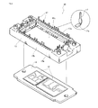
- Fig. 3 shows a perspective view of the semiconductor device 10 of Fig. 1
- Fig. 4 shows an exploded perspective view of Fig. 3
- the resin case 15 includes a bottom portion 15a and a side wall portion 15b, and has a practically rectangular form when seen from above, as shown in Fig. 3 .
- An aperture 15c is formed in a central portion of the bottom portion 15a of the resin case 15, as shown in the exploded perspective view of Fig. 4 .
- the heat releasing substrate 14 is fixed to the bottom portion 15a of the resin case 15 with the adhesive 16, as shown in Fig. 1 .
- the insulating circuit substrate 12 provided on the upper surface of the heat releasing substrate 14 is exposed through the aperture 15c of the resin case 15.
- a terminal 17 used as a main terminal or control terminal is provided inside the side wall portion 15b of the resin case 15.
- the terminal 17 shown in the drawing has an L-form, wherein one end, of a pin (rod) form, is exposed from the upper end of the side wall portion 15b of the resin case 15, while the other end, of a plate form, is exposed as a leg portion 17a from the inner surface side of the side wall portion 15b.
- copper, a copper alloy (brass, phosphor bronze, a C194 copper alloy, or the like), aluminum, a copper/aluminum clad material, or a copper-clad aluminum material can be used as a conductive material.
- a material wherein a conductive plating is applied to these conductive materials for the terminal 17.
- a reel terminal formed of these materials and wound into a reel wherein a plurality of terminals of the same form are linked. After forming the leg portion 17a of the terminal 17 by a process of bending the reel terminal, a plurality of the terminal 17 can be obtained by individually separating the terminals using a cutting process.
- the conductor layer 12b of the insulating circuit substrate 12, or the semiconductor chip 11, is electrically connected with bonding wire 18 to the leg portion 17a of the terminal 17 (refer to Fig. 1 ).
- the inside of the resin case 15, in which the bonding wire 18 is connected, is filled with a sealing resin 19 formed of a silicone resin, an epoxy resin, or the like.
- the semiconductor chip 11, terminal 17, conductor layer 12b, and the like, inside the resin case 15 are protected by the sealing resin 19.
- the resin case 15 in which the terminal 17 is provided is manufactured by a so-called insert molding wherein, after the terminal 17 is provided inside a molding die in which the resin case 15 is to be molded, resin is injected into the molding die, and the resin case 15 and terminal 17 are integrated by the terminal 17 being enveloped in the resin and the resin hardened.
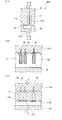
- FIG. 5A is a partial sectional view of a molding die in which is molded the vicinity of the side wall portion 15b of the resin case 15 shown in Fig. 1
- Fig. 5B is a partial sectional view of a B-B line of Fig. 5A
- Fig. 5C is a partial sectional view of a C-C line of Fig. 5A
- a molding die 20 is configured of an upper die 21 and lower die 22, and a cavity 23 is formed by the two coming into close contact.
- a plurality of the terminal 17 to be provided in the side wall portion 15b of the resin case 15 are individually held in the upper die 21.
- Protrusions 21a that fix each of the plurality of terminals 17 of the same form in a predetermined position are provided on the molding die on the side, of the upper die and lower die, on which the terminals are to be attached, which is the upper die 21 in this embodiment.
- the protrusions 21a are provided in positions corresponding to the vicinity of the base of the leg portions 17a of the terminals 17 held in the upper die 21, as shown in Figs. 5A and 5C .
- hole portions 30 holding the pin-form one end of the terminals 17 are provided at the same pitch as that of the protrusions 21a.
- Each of the plurality of terminals 17 of the same form is prepared in advance.
- the individual terminals 17 can be fabricated by, for example, separating the terminals using a cutting process after forming the leg portions 17a of the terminals 17 by a process of bending a reel terminal. Each of the separated terminals 17 is adjusted to the predetermined position by being sandwiched between protrusions 21a and inserted into the hole portions 30, whereby the terminals 17 are held in the upper die 21. Subsequently, the upper die 21 and lower die 22 are brought into close contact with each other, after which resin is injected into the cavity 23 of the molding die 20, thereby integrally molding the plurality of terminals 17 and the resin case 15.
- each of the plurality of terminals 17 being held in the upper die of the molding die 20, as heretofore described, there is no need for a terminal member of a configuration wherein terminals disposed in predetermined positions are connected with a tie bar to be fixed to the molding die, as is the case with a heretofore known insert molding.
- the terminals 17 are such that it is sufficient that individual terminals of the same form are manufactured from a thin plate of a conductive material, because of which the proportion of the portion of the thin plate of conductive material used for the terminals is high, and the terminal cost is low. Therefore, it is possible to reduce the terminal cost.
- the lower die 22 is standardized even when molding resin cases wherein the positions and number of the terminals 17 differ. That is, although different molding dies are needed for the upper die 21 in accordance with the positions and number of the terminals 17, it is sufficient to use the same molding die for the lower die 22. Consequently, as it is possible to standardize the lower die 22, it is possible to reduce the molding die cost in comparison with a heretofore known insert molding.
- the protrusions 21a of the upper die 21 shown in Figs. 5A to 5C are provided in order to hold each of the plurality of terminals 17 of the same form in the predetermined position.
- the protrusions 21a being provided, it is possible to prevent deviation in the positions of the terminals 17 due to the injection pressure when injecting resin into the molding die, and thus possible to reliably fix the terminals 17 in the predetermined positions.
- the protrusions 21a are provided in positions corresponding to the vicinity of the base of the leg portions 17a of the terminals 17 held in the upper die 21. Also, although it is possible to obtain the heretofore described advantages provided that at least one of the protrusions 21a is provided for one terminal 17 on the side supporting the terminal 17 against the direction of flow of the resin, it is preferable that a total of two protrusions 21a are provided, one on either side in the vicinity of the base of the leg portion 17a of the terminal 17.
- a molding die for molding the resin case 15 of the semiconductor device 10 of the invention is not limited to one wherein the length of the protrusion provided in the upper die is greater than the thickness of the leg portion 17a of the terminal 17.
- a modification example of a molding die for molding the resin case 15 is shown as partial sectional views in Figs. 6A to 6C .
- the same reference numbers are given to members the same as in Figs. 5A to 5C , and a redundant description will be omitted hereafter.
- a molding die 20A of Figs. 6A to 6C differs from the molding die 20 of Figs. 5A to 5C in that the length in a direction toward the lower die 22 of a protrusion 21b provided in the same position as the protrusion 21a provided in the upper die 21 of the molding die 20 in Figs. 5A to 5C is of the same extent as the thickness of the leg portion 17a of the terminal 17.
- the protrusion 21b positioned in front of the terminal 17 in Fig. 6A shown as an A-A line sectional view of Fig. 6C , is depicted as being of a length the same as the thickness of the leg portion 17a of the terminal 17, while the protrusion 21b neighboring the leg portion 17a of the terminal 17 is depicted as being of a length the same as the thickness of the leg portion 17a of the terminal 17 in Fig. 6C .
- the length of the protrusion 21b of the upper die 21D is short to the extent of being the same as the thickness of the leg portion 17a of the terminal 17.
- a modification example of a molding die wherein deviation in the position of the terminal 17 is prevented is shown as a partial sectional view in Fig. 7 .
- a molding die 24 shown in Fig. 7 is configured of an upper die 25 and the lower die 22, and a cavity 26 is formed by the two coming into close contact.
- a plurality of the terminal 17 are individually held in the upper die 25.
- a protrusion 25a is provided in a position corresponding to the vicinity of a leading end portion of the leg portion 17a of the terminal 17 in the upper die 25.
- protrusion 21a and protrusion 25a being provided in the upper die 25 in the modification example shown in Fig. 7 , it is not only possible to prevent deviation in the position of the terminal 17 in the vicinity of the base of the leg portion 17a, but also possible to prevent deviation in the position of the terminal 17 in the vicinity of the leading end portion of the leg portion 17a. Therefore, it is possible to more reliably fix the terminal 17 in the predetermined position.
- the length in a direction toward the lower die 22 of the protrusions 21a and 25a of Fig. 7 is greater than the thickness of the leg portion 17a of the terminal 17, the example shown in the drawing is not limiting.
- the length in a direction toward the lower die 22 of the protrusions 21a and 25a of Fig. 7 may be of the same extent as the thickness of the leg portion 17a of the terminal 17, in the same way as the protrusion 21b of Figs. 6A to 6C .
- FIG. 8 Another modification example of a molding die wherein deviation in the position of the terminal 17 is prevented is shown as a partial sectional view in Fig. 8 .
- a molding die 27 shown in Fig. 8 is configured of the upper die 21 and a lower die 28, and a cavity 29 is formed by the two coming into close contact.
- a plurality of the terminal 17 are individually held in the upper die 21.
- the molding die 27 shown in Fig. 8 with the molding die 20 shown in Fig. 5A , it differs in that, in addition to the protrusion 21a being provided, a leading end portion of the leg portion 17a of the terminal 17 is clamped by the upper die 21 and lower die 28.
- the length in a direction toward the lower die 22 of the protrusion 21a of Fig. 8 is greater than the thickness of the leg portion 17a of the terminal 17, the example shown in the drawing is not limiting.
- the length in a direction toward the lower die 22 of the protrusion 21a of Fig. 8 may be of the same extent as the thickness of the leg portion 17a of the terminal 17, in the same way as the protrusion 21b of Figs. 6A to 6C .
- the terminals 17 When holding the plurality of terminals 17 in the heretofore described molding die 20, 20A, 24, or 27, the terminals 17 may be held one by one, but in this case, the number of holding operations increases in direct proportion to the number of terminals. Because of this, there is concern about the operation cost increasing, and mass productivity deteriorating. Therefore, it is preferable that all the terminals 17 to be held in one molding die are held at one time, as it is thus possible to reduce the operation cost. In order that all the terminals 17 are held at one time, for example, the following is carried out.
- a jig (receiving jig), into which a plurality of the terminal 17 can be inserted and held in the same predetermined positions as those in which they are to be held in the molding die, and to the same predetermined quantity, and a jig (transfer jig), which can move the plurality of terminals 17 held in the receiving jig at one time with the positions and quantity as they are, are prepared in advance.
- the plurality of terminals 17 are held in the predetermined positions and to the predetermined quantity in the receiving jig, and next, the plurality of terminals 17 held in the receiving jig are held in the molding die 20, 20A, 24, or 27, all at one time, by the transfer jig.
- the transfer jig is a jig such that, for example, the terminals 17 can be temporarily fixed to the transfer jig by air adsorption or mechanical gripping.
- the resin case 15 provided with the terminal 17 and manufactured in the way heretofore described is joined with the adhesive 16 to an assembly of the semiconductor chip 11, insulating circuit substrate 12, and heat releasing substrate 14 in the semiconductor device 10 of Fig. 1 .
- the terminal 17 is wire-bonded with the bonding wire 18 to the conductor layer 12b of the insulating circuit substrate 12 or to the semiconductor chip 11.
- the inside of the resin case 15 is filled with the sealing resin 19.
- Fig. 9A is a partial plan view of the side wall portion 15b of the resin case 15
- Fig. 9B is a partial side view of the side wall portion 15b seen from the inner surface side
- Fig. 9C is a partial sectional view cut along an X-X line of Fig. 9A .
- the resin case 15 shown is formed by the resin case 15 and plurality of terminals 17 being integrally molded.
- the resin case 15 is such that protrusion marks 15d are formed as depressed portions in the vicinity of the base of the leg portion 17a of the terminals 17.
- the protrusion marks 15d are formed by the protrusions 21a provided in the upper die 21 of the molding die 20.
- Fig. 10A is a partial plan view of the side wall portion 15b of a resin case 15G
- Fig. 10B is a partial side view of the side wall portion 15b seen from the inner surface side
- Fig. 10C is a partial sectional view cut along an X-X line of Fig. 10A
- the resin case 15G shown is formed by the resin case 15G and plurality of terminals 17 being integrally molded.
- the resin case 15G is such that protrusion marks 15f are formed as depressed portions in the vicinity of the base of the leg portion 17a of the terminals 17.
- the protrusion marks 15f are formed by the protrusions 21b provided in the upper die 21D of the molding die 20A.
- Fig. 11A is a partial plan view of a side wall portion 35b of a resin case 35
- Fig. 11B is a partial sectional view cut along an X-X line of Fig. 11A .
- the resin case 35 shown in Figs. 11A and 11B with the resin case 15 shown in Figs. 9A to 9C , it differs in that, in addition to the protrusion marks 15d being formed in the vicinity of the base of the leg portion 17a of the terminals 17, protrusion marks 15e are formed in the vicinity of the leading end portion of the leg portions 17a.
- the protrusion marks 15e are formed by the protrusions 25a provided in the upper die 25 of the molding die 24.
- FIG. 12A is a sectional view of a side wall portion 45b of a resin case 45
- Fig. 12B is a partial sectional view cut along an X-X line of Fig. 12A .
- the leading end portion of the leg portion 17a is such that not only the front surface, to which the bonding wire 18 is joined, but also the back surface is exposed from the resin case 45.
- the leading end portion of the leg portion 17a being exposed on the front and back surfaces is because of the vicinity of the leading end portion of the leg portion 17a being clamped by the upper die 21 and lower die 28 of the molding die 27.
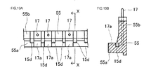
- FIG. 13A is a sectional view of a side wall portion 55b of a resin case 55
- Fig. 13B is a partial sectional view cut along an X-X line of Fig. 13A .
- the resin case 55 shown in Figs. 13A and 13B with the resin case 15 shown in Fig. 9C , it differs in that the thickness of the side wall portion 55b in the vicinity of the base of the leg portion 17a of the terminal 17 is greater than that of the upper side of the side wall portion 55b.
- the thickness of the side wall portion 55b in the vicinity of the base of the leg portion 17a being greater than that of the upper side of the side wall portion 55b, it is possible to increase the strength of the side wall portion in the vicinity of the base of the leg portion 17a.
- All of the resin cases 15, 15G, 35, 45, and 55 can be manufactured using one kind of resin chosen from a polyphenylene sulfide resin (PPS resin), a polybutylene terephthalate resin (PBT resin), a polyamide resin (PA resin), or an acrylonitrile butadiene styrene resin (ABS resin), and it is thus possible to provide superior electrical insulating properties.
- Sides of leg portion 17a of terminal 17 are partially exposed in areas of protrusion marks 15d, 15e, 15f. It becomes easy to check whether or not terminal 17 is fixed in place by observing a position of the exposed side in protrusion marks.
- thermo-setting resin such as epoxy resin is used for encapsulation resin 19
- terminal 17 is solidly fixed between resin case 15 and encapsulation resin 19 because of an anchor effect of the resin.
- terminals of differing forms are used as main terminals and control terminals, and molding is carried out with a molding die in which are provided protrusions for holding each of the terminals in a predetermined position, it is possible to provide at low cost a semiconductor device manufacturing method whereby terminals of differing forms are included, and it is possible to respond to differing terminal arrays.
Landscapes
- Encapsulation Of And Coatings For Semiconductor Or Solid State Devices (AREA)
- Structures Or Materials For Encapsulating Or Coating Semiconductor Devices Or Solid State Devices (AREA)
Applications Claiming Priority (1)
| Application Number | Priority Date | Filing Date | Title |
|---|---|---|---|
| JP2013087899A JP6107362B2 (ja) | 2013-04-18 | 2013-04-18 | 半導体装置の製造方法及び半導体装置 |
Publications (3)
| Publication Number | Publication Date |
|---|---|
| EP2793256A2 true EP2793256A2 (de) | 2014-10-22 |
| EP2793256A3 EP2793256A3 (de) | 2016-04-06 |
| EP2793256B1 EP2793256B1 (de) | 2021-01-13 |
Family
ID=50732781
Family Applications (1)
| Application Number | Title | Priority Date | Filing Date |
|---|---|---|---|
| EP14164833.7A Active EP2793256B1 (de) | 2013-04-18 | 2014-04-16 | Methode zur Herstellung eines Halbleiterbauelements |
Country Status (4)
| Country | Link |
|---|---|
| US (2) | US9070696B2 (de) |
| EP (1) | EP2793256B1 (de) |
| JP (1) | JP6107362B2 (de) |
| CN (1) | CN104167370B (de) |
Families Citing this family (12)
| Publication number | Priority date | Publication date | Assignee | Title |
|---|---|---|---|---|
| JP6299120B2 (ja) * | 2013-09-05 | 2018-03-28 | 富士電機株式会社 | 半導体モジュール |
| JP6451257B2 (ja) * | 2014-11-21 | 2019-01-16 | 富士電機株式会社 | 半導体装置 |
| KR102425694B1 (ko) * | 2015-03-17 | 2022-07-27 | 주식회사 솔루엠 | 파워 모듈 패키지 |
| JP6547354B2 (ja) * | 2015-03-20 | 2019-07-24 | 富士電機株式会社 | 半導体モジュールおよび樹脂ケース |
| JP6645134B2 (ja) * | 2015-11-16 | 2020-02-12 | 富士電機株式会社 | 半導体装置および半導体装置の製造方法 |
| JP6984127B2 (ja) * | 2016-12-28 | 2021-12-17 | 富士電機株式会社 | 半導体装置および半導体装置の製造方法 |
| JP6988161B2 (ja) * | 2017-05-17 | 2022-01-05 | 富士電機株式会社 | パワー半導体モジュールおよびパワー半導体装置 |
| CN111148338A (zh) * | 2018-11-01 | 2020-05-12 | 邱昱维 | 在布局有电路的陶瓷基板上成形环绕壁的方法及该基板 |
| JP7318238B2 (ja) * | 2019-03-11 | 2023-08-01 | 富士電機株式会社 | 半導体装置 |
| CN111916361A (zh) * | 2019-05-10 | 2020-11-10 | 中芯长电半导体(江阴)有限公司 | 一种塑封模具及塑封方法 |
| JP7313302B2 (ja) * | 2020-03-18 | 2023-07-24 | 三菱電機株式会社 | 半導体装置および半導体装置の製造方法 |
| JP7353255B2 (ja) * | 2020-10-30 | 2023-09-29 | 三菱電機株式会社 | 半導体装置用の筐体の製造方法 |
Citations (4)
| Publication number | Priority date | Publication date | Assignee | Title |
|---|---|---|---|---|
| JPH098223A (ja) | 1995-06-16 | 1997-01-10 | Mitsubishi Electric Corp | 半導体パワーモジュールおよびその製造方法 |
| JP2004134518A (ja) | 2002-10-09 | 2004-04-30 | Nissan Motor Co Ltd | 電子部品、電子部品の製造方法及び製造装置 |
| JP2008252055A (ja) | 2007-03-08 | 2008-10-16 | Fuji Electric Device Technology Co Ltd | 半導体装置およびその製造方法 |
| JP2009021286A (ja) | 2007-07-10 | 2009-01-29 | Mitsubishi Electric Corp | 電力用半導体装置 |
Family Cites Families (5)
| Publication number | Priority date | Publication date | Assignee | Title |
|---|---|---|---|---|
| JP2705368B2 (ja) * | 1991-05-31 | 1998-01-28 | 株式会社デンソー | 電子装置 |
| CN1248376C (zh) * | 2001-11-08 | 2006-03-29 | 莫列斯公司 | 电连接器的制造方法及其制品 |
| JP4141789B2 (ja) * | 2002-10-11 | 2008-08-27 | 三菱電機株式会社 | 電力用半導体装置 |
| DE102004054597B4 (de) * | 2004-11-11 | 2019-07-25 | Infineon Technologies Ag | Elektronisches Bauteil und Verfahren zum Herstellen eines elektronischen Bauteils |
| US7944042B2 (en) | 2007-03-08 | 2011-05-17 | Fuji Electric Device Technology Co., Ltd. | Semiconductor device and method of manufacturing same |
-
2013
- 2013-04-18 JP JP2013087899A patent/JP6107362B2/ja active Active
-
2014
- 2014-04-10 CN CN201410142784.1A patent/CN104167370B/zh active Active
- 2014-04-11 US US14/251,036 patent/US9070696B2/en active Active
- 2014-04-16 EP EP14164833.7A patent/EP2793256B1/de active Active
-
2015
- 2015-05-18 US US14/715,018 patent/US9466509B2/en active Active
Patent Citations (4)
| Publication number | Priority date | Publication date | Assignee | Title |
|---|---|---|---|---|
| JPH098223A (ja) | 1995-06-16 | 1997-01-10 | Mitsubishi Electric Corp | 半導体パワーモジュールおよびその製造方法 |
| JP2004134518A (ja) | 2002-10-09 | 2004-04-30 | Nissan Motor Co Ltd | 電子部品、電子部品の製造方法及び製造装置 |
| JP2008252055A (ja) | 2007-03-08 | 2008-10-16 | Fuji Electric Device Technology Co Ltd | 半導体装置およびその製造方法 |
| JP2009021286A (ja) | 2007-07-10 | 2009-01-29 | Mitsubishi Electric Corp | 電力用半導体装置 |
Also Published As
| Publication number | Publication date |
|---|---|
| US9466509B2 (en) | 2016-10-11 |
| EP2793256A3 (de) | 2016-04-06 |
| CN104167370A (zh) | 2014-11-26 |
| US9070696B2 (en) | 2015-06-30 |
| US20140312464A1 (en) | 2014-10-23 |
| CN104167370B (zh) | 2018-10-23 |
| US20150249023A1 (en) | 2015-09-03 |
| EP2793256B1 (de) | 2021-01-13 |
| JP2014212218A (ja) | 2014-11-13 |
| JP6107362B2 (ja) | 2017-04-05 |
Similar Documents
| Publication | Publication Date | Title |
|---|---|---|
| EP2793256B1 (de) | Methode zur Herstellung eines Halbleiterbauelements | |
| JP5252819B2 (ja) | 半導体装置およびその製造方法 | |
| EP3226292B1 (de) | Leiterrahmen, halbleiterbauelement, verfahren zur herstellung eines leiterrahmens und verfahren zur herstellung eines halbleiterbauelements | |
| US20200211937A1 (en) | Semiconductor device and method for producing semiconductor device | |
| US9437527B2 (en) | Method for manufacturing electrical connections in a semiconductor device and the semiconductor device | |
| US10840172B2 (en) | Leadframe, semiconductor package including a leadframe and method for forming a semiconductor package | |
| US20150137279A1 (en) | Multi-die sensor device | |
| US8664946B2 (en) | Sensor packages including a lead frame and moulding body and methods of manufacturing | |
| JP6673012B2 (ja) | 半導体装置およびその製造方法 | |
| US10957633B2 (en) | Semiconductor device packaging assembly, lead frame strip and unit lead frame with trenches or grooves for guiding liquefied molding material | |
| US10586773B2 (en) | Semiconductor device | |
| US8981541B2 (en) | Quad flat semiconductor device with additional contacts | |
| US20140175626A1 (en) | Integrated circuit package and method of manufacture | |
| US8471370B2 (en) | Semiconductor element with semiconductor die and lead frames | |
| JP2009094189A (ja) | コネクタ付き半導体パッケージ | |
| US10854540B2 (en) | Packaged IC component | |
| JP2023157585A (ja) | 半導体装置 | |
| JP2005328009A (ja) | チップパッケージ、該チップパッケージの製造方法およびチップ実装基板 | |
| JP2015037103A (ja) | 半導体装置及び半導体装置の製造方法 | |
| CN100446199C (zh) | 用于电子部件的引线框架及其制造的方法 | |
| US20240332145A1 (en) | Clips with alignment features and related methods | |
| US7074654B1 (en) | Tape supported memory card leadframe structure | |
| JP2008098506A (ja) | コイル部品及びコイル部品の製造方法 | |
| JPS6143857B2 (de) | ||
| JPH0736430B2 (ja) | 樹脂封止形半導体装置の製造方法 |
Legal Events
| Date | Code | Title | Description |
|---|---|---|---|
| PUAI | Public reference made under article 153(3) epc to a published international application that has entered the european phase |
Free format text: ORIGINAL CODE: 0009012 |
|
| 17P | Request for examination filed |
Effective date: 20140416 |
|
| AK | Designated contracting states |
Kind code of ref document: A2 Designated state(s): AL AT BE BG CH CY CZ DE DK EE ES FI FR GB GR HR HU IE IS IT LI LT LU LV MC MK MT NL NO PL PT RO RS SE SI SK SM TR |
|
| AX | Request for extension of the european patent |
Extension state: BA ME |
|
| PUAL | Search report despatched |
Free format text: ORIGINAL CODE: 0009013 |
|
| AK | Designated contracting states |
Kind code of ref document: A3 Designated state(s): AL AT BE BG CH CY CZ DE DK EE ES FI FR GB GR HR HU IE IS IT LI LT LU LV MC MK MT NL NO PL PT RO RS SE SI SK SM TR |
|
| AX | Request for extension of the european patent |
Extension state: BA ME |
|
| RIC1 | Information provided on ipc code assigned before grant |
Ipc: H01L 23/498 20060101ALI20160301BHEP Ipc: H01L 23/24 20060101ALN20160301BHEP Ipc: H01L 23/00 20060101AFI20160301BHEP Ipc: H01L 21/56 20060101ALI20160301BHEP Ipc: H01L 23/544 20060101ALI20160301BHEP Ipc: H01L 23/057 20060101ALI20160301BHEP |
|
| R17P | Request for examination filed (corrected) |
Effective date: 20161006 |
|
| RBV | Designated contracting states (corrected) |
Designated state(s): AL AT BE BG CH CY CZ DE DK EE ES FI FR GB GR HR HU IE IS IT LI LT LU LV MC MK MT NL NO PL PT RO RS SE SI SK SM TR |
|
| STAA | Information on the status of an ep patent application or granted ep patent |
Free format text: STATUS: EXAMINATION IS IN PROGRESS |
|
| 17Q | First examination report despatched |
Effective date: 20190402 |
|
| GRAP | Despatch of communication of intention to grant a patent |
Free format text: ORIGINAL CODE: EPIDOSNIGR1 |
|
| STAA | Information on the status of an ep patent application or granted ep patent |
Free format text: STATUS: GRANT OF PATENT IS INTENDED |
|
| RIC1 | Information provided on ipc code assigned before grant |
Ipc: H01L 23/057 20060101ALI20200708BHEP Ipc: H01L 23/544 20060101ALI20200708BHEP Ipc: H01L 23/24 20060101ALN20200708BHEP Ipc: H01L 23/498 20060101ALI20200708BHEP Ipc: H01L 25/00 20060101ALI20200708BHEP Ipc: H01L 21/56 20060101ALI20200708BHEP Ipc: H01L 23/00 20060101AFI20200708BHEP |
|
| INTG | Intention to grant announced |
Effective date: 20200723 |
|
| GRAS | Grant fee paid |
Free format text: ORIGINAL CODE: EPIDOSNIGR3 |
|
| GRAA | (expected) grant |
Free format text: ORIGINAL CODE: 0009210 |
|
| STAA | Information on the status of an ep patent application or granted ep patent |
Free format text: STATUS: THE PATENT HAS BEEN GRANTED |
|
| AK | Designated contracting states |
Kind code of ref document: B1 Designated state(s): AL AT BE BG CH CY CZ DE DK EE ES FI FR GB GR HR HU IE IS IT LI LT LU LV MC MK MT NL NO PL PT RO RS SE SI SK SM TR |
|
| REG | Reference to a national code |
Ref country code: GB Ref legal event code: FG4D |
|
| REG | Reference to a national code |
Ref country code: CH Ref legal event code: EP |
|
| REG | Reference to a national code |
Ref country code: DE Ref legal event code: R096 Ref document number: 602014074171 Country of ref document: DE |
|
| REG | Reference to a national code |
Ref country code: IE Ref legal event code: FG4D |
|
| REG | Reference to a national code |
Ref country code: AT Ref legal event code: REF Ref document number: 1355174 Country of ref document: AT Kind code of ref document: T Effective date: 20210215 |
|
| REG | Reference to a national code |
Ref country code: AT Ref legal event code: MK05 Ref document number: 1355174 Country of ref document: AT Kind code of ref document: T Effective date: 20210113 |
|
| REG | Reference to a national code |
Ref country code: NL Ref legal event code: MP Effective date: 20210113 |
|
| REG | Reference to a national code |
Ref country code: LT Ref legal event code: MG9D |
|
| PG25 | Lapsed in a contracting state [announced via postgrant information from national office to epo] |
Ref country code: FI Free format text: LAPSE BECAUSE OF FAILURE TO SUBMIT A TRANSLATION OF THE DESCRIPTION OR TO PAY THE FEE WITHIN THE PRESCRIBED TIME-LIMIT Effective date: 20210113 Ref country code: HR Free format text: LAPSE BECAUSE OF FAILURE TO SUBMIT A TRANSLATION OF THE DESCRIPTION OR TO PAY THE FEE WITHIN THE PRESCRIBED TIME-LIMIT Effective date: 20210113 Ref country code: GR Free format text: LAPSE BECAUSE OF FAILURE TO SUBMIT A TRANSLATION OF THE DESCRIPTION OR TO PAY THE FEE WITHIN THE PRESCRIBED TIME-LIMIT Effective date: 20210414 Ref country code: PT Free format text: LAPSE BECAUSE OF FAILURE TO SUBMIT A TRANSLATION OF THE DESCRIPTION OR TO PAY THE FEE WITHIN THE PRESCRIBED TIME-LIMIT Effective date: 20210513 Ref country code: LT Free format text: LAPSE BECAUSE OF FAILURE TO SUBMIT A TRANSLATION OF THE DESCRIPTION OR TO PAY THE FEE WITHIN THE PRESCRIBED TIME-LIMIT Effective date: 20210113 Ref country code: NL Free format text: LAPSE BECAUSE OF FAILURE TO SUBMIT A TRANSLATION OF THE DESCRIPTION OR TO PAY THE FEE WITHIN THE PRESCRIBED TIME-LIMIT Effective date: 20210113 Ref country code: NO Free format text: LAPSE BECAUSE OF FAILURE TO SUBMIT A TRANSLATION OF THE DESCRIPTION OR TO PAY THE FEE WITHIN THE PRESCRIBED TIME-LIMIT Effective date: 20210413 Ref country code: BG Free format text: LAPSE BECAUSE OF FAILURE TO SUBMIT A TRANSLATION OF THE DESCRIPTION OR TO PAY THE FEE WITHIN THE PRESCRIBED TIME-LIMIT Effective date: 20210413 |
|
| PG25 | Lapsed in a contracting state [announced via postgrant information from national office to epo] |
Ref country code: RS Free format text: LAPSE BECAUSE OF FAILURE TO SUBMIT A TRANSLATION OF THE DESCRIPTION OR TO PAY THE FEE WITHIN THE PRESCRIBED TIME-LIMIT Effective date: 20210113 Ref country code: LV Free format text: LAPSE BECAUSE OF FAILURE TO SUBMIT A TRANSLATION OF THE DESCRIPTION OR TO PAY THE FEE WITHIN THE PRESCRIBED TIME-LIMIT Effective date: 20210113 Ref country code: PL Free format text: LAPSE BECAUSE OF FAILURE TO SUBMIT A TRANSLATION OF THE DESCRIPTION OR TO PAY THE FEE WITHIN THE PRESCRIBED TIME-LIMIT Effective date: 20210113 Ref country code: AT Free format text: LAPSE BECAUSE OF FAILURE TO SUBMIT A TRANSLATION OF THE DESCRIPTION OR TO PAY THE FEE WITHIN THE PRESCRIBED TIME-LIMIT Effective date: 20210113 Ref country code: SE Free format text: LAPSE BECAUSE OF FAILURE TO SUBMIT A TRANSLATION OF THE DESCRIPTION OR TO PAY THE FEE WITHIN THE PRESCRIBED TIME-LIMIT Effective date: 20210113 |
|
| PG25 | Lapsed in a contracting state [announced via postgrant information from national office to epo] |
Ref country code: IS Free format text: LAPSE BECAUSE OF FAILURE TO SUBMIT A TRANSLATION OF THE DESCRIPTION OR TO PAY THE FEE WITHIN THE PRESCRIBED TIME-LIMIT Effective date: 20210513 |
|
| REG | Reference to a national code |
Ref country code: DE Ref legal event code: R097 Ref document number: 602014074171 Country of ref document: DE |
|
| PG25 | Lapsed in a contracting state [announced via postgrant information from national office to epo] |
Ref country code: SM Free format text: LAPSE BECAUSE OF FAILURE TO SUBMIT A TRANSLATION OF THE DESCRIPTION OR TO PAY THE FEE WITHIN THE PRESCRIBED TIME-LIMIT Effective date: 20210113 Ref country code: CZ Free format text: LAPSE BECAUSE OF FAILURE TO SUBMIT A TRANSLATION OF THE DESCRIPTION OR TO PAY THE FEE WITHIN THE PRESCRIBED TIME-LIMIT Effective date: 20210113 Ref country code: EE Free format text: LAPSE BECAUSE OF FAILURE TO SUBMIT A TRANSLATION OF THE DESCRIPTION OR TO PAY THE FEE WITHIN THE PRESCRIBED TIME-LIMIT Effective date: 20210113 |
|
| PLBE | No opposition filed within time limit |
Free format text: ORIGINAL CODE: 0009261 |
|
| STAA | Information on the status of an ep patent application or granted ep patent |
Free format text: STATUS: NO OPPOSITION FILED WITHIN TIME LIMIT |
|
| PG25 | Lapsed in a contracting state [announced via postgrant information from national office to epo] |
Ref country code: DK Free format text: LAPSE BECAUSE OF FAILURE TO SUBMIT A TRANSLATION OF THE DESCRIPTION OR TO PAY THE FEE WITHIN THE PRESCRIBED TIME-LIMIT Effective date: 20210113 Ref country code: ES Free format text: LAPSE BECAUSE OF FAILURE TO SUBMIT A TRANSLATION OF THE DESCRIPTION OR TO PAY THE FEE WITHIN THE PRESCRIBED TIME-LIMIT Effective date: 20210113 Ref country code: MC Free format text: LAPSE BECAUSE OF FAILURE TO SUBMIT A TRANSLATION OF THE DESCRIPTION OR TO PAY THE FEE WITHIN THE PRESCRIBED TIME-LIMIT Effective date: 20210113 Ref country code: SK Free format text: LAPSE BECAUSE OF FAILURE TO SUBMIT A TRANSLATION OF THE DESCRIPTION OR TO PAY THE FEE WITHIN THE PRESCRIBED TIME-LIMIT Effective date: 20210113 Ref country code: RO Free format text: LAPSE BECAUSE OF FAILURE TO SUBMIT A TRANSLATION OF THE DESCRIPTION OR TO PAY THE FEE WITHIN THE PRESCRIBED TIME-LIMIT Effective date: 20210113 |
|
| 26N | No opposition filed |
Effective date: 20211014 |
|
| GBPC | Gb: european patent ceased through non-payment of renewal fee |
Effective date: 20210416 |
|
| PG25 | Lapsed in a contracting state [announced via postgrant information from national office to epo] |
Ref country code: LU Free format text: LAPSE BECAUSE OF NON-PAYMENT OF DUE FEES Effective date: 20210416 |
|
| REG | Reference to a national code |
Ref country code: BE Ref legal event code: MM Effective date: 20210430 |
|
| PG25 | Lapsed in a contracting state [announced via postgrant information from national office to epo] |
Ref country code: LI Free format text: LAPSE BECAUSE OF NON-PAYMENT OF DUE FEES Effective date: 20210430 Ref country code: CH Free format text: LAPSE BECAUSE OF NON-PAYMENT OF DUE FEES Effective date: 20210430 Ref country code: AL Free format text: LAPSE BECAUSE OF FAILURE TO SUBMIT A TRANSLATION OF THE DESCRIPTION OR TO PAY THE FEE WITHIN THE PRESCRIBED TIME-LIMIT Effective date: 20210113 Ref country code: FR Free format text: LAPSE BECAUSE OF NON-PAYMENT OF DUE FEES Effective date: 20210430 Ref country code: GB Free format text: LAPSE BECAUSE OF NON-PAYMENT OF DUE FEES Effective date: 20210416 |
|
| PG25 | Lapsed in a contracting state [announced via postgrant information from national office to epo] |
Ref country code: SI Free format text: LAPSE BECAUSE OF FAILURE TO SUBMIT A TRANSLATION OF THE DESCRIPTION OR TO PAY THE FEE WITHIN THE PRESCRIBED TIME-LIMIT Effective date: 20210113 |
|
| PG25 | Lapsed in a contracting state [announced via postgrant information from national office to epo] |
Ref country code: IT Free format text: LAPSE BECAUSE OF FAILURE TO SUBMIT A TRANSLATION OF THE DESCRIPTION OR TO PAY THE FEE WITHIN THE PRESCRIBED TIME-LIMIT Effective date: 20210113 Ref country code: IE Free format text: LAPSE BECAUSE OF NON-PAYMENT OF DUE FEES Effective date: 20210416 |
|
| PG25 | Lapsed in a contracting state [announced via postgrant information from national office to epo] |
Ref country code: IS Free format text: LAPSE BECAUSE OF FAILURE TO SUBMIT A TRANSLATION OF THE DESCRIPTION OR TO PAY THE FEE WITHIN THE PRESCRIBED TIME-LIMIT Effective date: 20210513 |
|
| PG25 | Lapsed in a contracting state [announced via postgrant information from national office to epo] |
Ref country code: BE Free format text: LAPSE BECAUSE OF NON-PAYMENT OF DUE FEES Effective date: 20210430 |
|
| PG25 | Lapsed in a contracting state [announced via postgrant information from national office to epo] |
Ref country code: HU Free format text: LAPSE BECAUSE OF FAILURE TO SUBMIT A TRANSLATION OF THE DESCRIPTION OR TO PAY THE FEE WITHIN THE PRESCRIBED TIME-LIMIT; INVALID AB INITIO Effective date: 20140416 |
|
| PG25 | Lapsed in a contracting state [announced via postgrant information from national office to epo] |
Ref country code: CY Free format text: LAPSE BECAUSE OF FAILURE TO SUBMIT A TRANSLATION OF THE DESCRIPTION OR TO PAY THE FEE WITHIN THE PRESCRIBED TIME-LIMIT Effective date: 20210113 |
|
| PG25 | Lapsed in a contracting state [announced via postgrant information from national office to epo] |
Ref country code: MK Free format text: LAPSE BECAUSE OF FAILURE TO SUBMIT A TRANSLATION OF THE DESCRIPTION OR TO PAY THE FEE WITHIN THE PRESCRIBED TIME-LIMIT Effective date: 20210113 |
|
| PG25 | Lapsed in a contracting state [announced via postgrant information from national office to epo] |
Ref country code: MT Free format text: LAPSE BECAUSE OF FAILURE TO SUBMIT A TRANSLATION OF THE DESCRIPTION OR TO PAY THE FEE WITHIN THE PRESCRIBED TIME-LIMIT Effective date: 20210113 |
|
| PGFP | Annual fee paid to national office [announced via postgrant information from national office to epo] |
Ref country code: DE Payment date: 20250305 Year of fee payment: 12 |
|
| REG | Reference to a national code |
Ref country code: DE Ref legal event code: R079 Ref document number: 602014074171 Country of ref document: DE Free format text: PREVIOUS MAIN CLASS: H01L0023000000 Ipc: H10W0099000000 |
|
| PG25 | Lapsed in a contracting state [announced via postgrant information from national office to epo] |
Ref country code: TR Free format text: LAPSE BECAUSE OF FAILURE TO SUBMIT A TRANSLATION OF THE DESCRIPTION OR TO PAY THE FEE WITHIN THE PRESCRIBED TIME-LIMIT Effective date: 20210113 |